Article

Enhanced Electrochromic Properties by Improvement of Crystallinity for Sputtered WO3 Film

1
Institute of Advanced Wear and Corrosion Resistant and Functional Materials, Jinan University, Guangzhou 510632, China
2
The Key Lab of Guangdong for Modern Surface Engineering, National Engineering Laboratory for Modern Materials Surface Engineering Technology, Guangdong Institute of New Materials, Guangdong Academy of Science, Guangzhou 510651, China
3
Guangdong Provincial Key Laboratory of Advanced Energy Storage Materials, South China University of Technology, Guangzhou 510641, China
*
Authors to whom correspondence should be addressed.
Coatings 2020, 10(6), 577; https://doi.org/10.3390/coatings10060577
Submission received: 13 May 2020 / Revised: 16 June 2020 / Accepted: 18 June 2020 / Published: 19 June 2020
(This article belongs to the Special Issue Advanced Thin Films Deposited by Magnetron Sputtering)

Abstract

:
Tungsten oxide (WO3) is widely used as a functional material for “smart windows” due to its excellent electrochromic properties, however it is difficult to overcome the conflict between its optical modulation and cyclic stability. In this work, WO3 thin films with different crystal structures were prepared by DC reactive magnetron sputtering method. The effects of substrate temperature on the structure, composition, and electrochromic properties of WO3 films were investigated. The results show that the crystallinity of the WO3 film increases with increasing deposition temperature, indicating that temperature plays an important role in controlling the structure of the WO3 film. For WO3 thin films formed at a substrate temperature of 573 K, the film is in an amorphous state to a crystalline transition state. From X-ray diffraction (XRD) analysis, the thin film showed a weak WO3 crystallization peak, which was in the composite structure of amorphous and nanocrystalline. Which has the best electrochromic properties, with modulation amplitude of 73.1% and bleached state with a coloration efficiency of 42.9 cm2/C at a wavelength of 550 nm. Even after 1500 cycles, the optical modulation still contains 65.4%, delivering the best cyclic stability.

1. Introduction

With the increase of global challenges related to energy depletion, the development of new energy-saving materials, such as electrochromic (EC) materials attracting people’s attention [1,2,3]. Electrochromic materials are capable of reversibly changing their optical properties by switching the applied voltage [4,5,6]. Owing to their large optical modulation range and long cycle life, the EC materials can be used as a smart window for energy-saving buildings or antiglare rear-view mirrors for automobiles. Tungsten trioxide is considered to be a promising EC material, which achieves high optical modulation from transparency to blue by lithium ion and electron injection/extraction [7,8,9,10,11].
Magnetron sputtering is the most promising technology for WO3 thin film preparation. Studies have shown that the electrochromic performance of WO3 thin films is closely related to its structure, including geometry, particle size, crystallinity, stoichiometry, etc. [12,13]. It is widely believed that crystalline WO3 thin films have remarkable cyclic stability and low optical modulation range, while the amorphous ones show the opposite characteristics [14,15]. Researchers have been devoted to balancing the different EC properties between amorphous and crystalline WO3 films [16]. For example, Gaurav M. et al. [17] prepared nanoporous γ-WO3 thin films by DC reactive magnetron sputtering and subsequent heat treatment. The results show that its light modulation is 46%, good cyclic stability at least up to 500 cycles. However, the results are still unsatisfactory because of nonindustrial post annealing process, in situ preparation and poor EC performance. Related researchers are concerned about how to improve the crystalline characteristics of the film to obtain high EC performance. Such as, Madhavi V. et al. [18] tried to improve the crystallinity of WO3 films by adjusting substrate temperature during RF reactive magnetron sputtering process, however the poor optical modulation of 40% and coloration efficiency of 33.8 cm2/C were obtained.
The magnetron sputtering method has been widely used to prepare oxide films with adjustable microstructure and crystalline structure. In this study, WO3 thin films with intermediate states between amorphous and nanocrystalline were prepared by DC reactive magnetron sputtering [19]. The structure, composition, and electrochromic properties of WO3 films with different crystallinity were obtained and their impact on performance was discussed. Based on the different substrate temperature during deposition, we are trying to reveal the relationship between the crystal level and EC properties.

2. Materials and Methods

Tungsten trioxide thin films were grown on In2O3:Sn (ITO film sheet resistance of about 8 Ω) coated glass substrates by DC reactive magnetron sputtering technique using pure metallic tungsten target (76.2 mm diameter and 3 mm thickness). The base pressure is pumped to below 8.0 × 10⁻⁴ Pa, then the O2 and Ar (99.99% purity) gas with a ratio of 1:1 are applied as reaction gas and sputtering gas. During deposition, the sputtering power and working pressure were kept at 270 W and 3 Pa respectively. The target–substrate distance was 76.5 mm. To obtain the different crystallinity of WO3 thin films, the films were prepared at substrate temperatures of 300, 473, 573, 673 and 743 K, respectively.
The crystallographic structure of films was analyzed by X-ray diffraction (XRD, D8 Advance X, Bruker, Karlsruhe, Germany), using Cu-Kα as target with scanning range of 20–80° and step size of 0.05°. The film composition, bonding energy and bonding state of tungsten and oxygen were measured by X-ray photoelectron spectroscopy (XPS, AXIS Supra, Shimadzu, Tokyo, Japan). The microstructure and morphology of the films were characterized by field emission scanning electron microscope (FESEM, SU8220, Hitachi, Tokyo, Japan) and atomic force microscope (AFM, Dimension edge, Bruker, Karlsruhe, Germany). The transmittance of the thin film was measured by an ultraviolet-visible spectrophotometer (SP-752PC, Spectrum, Shanghai, China) with a wavelength range of 300–800 nm. The electrochromic and electrochemical performance were tested by electrochemical workstation (P4000, Princeton, NJ, USA).

3. Results and Discussion

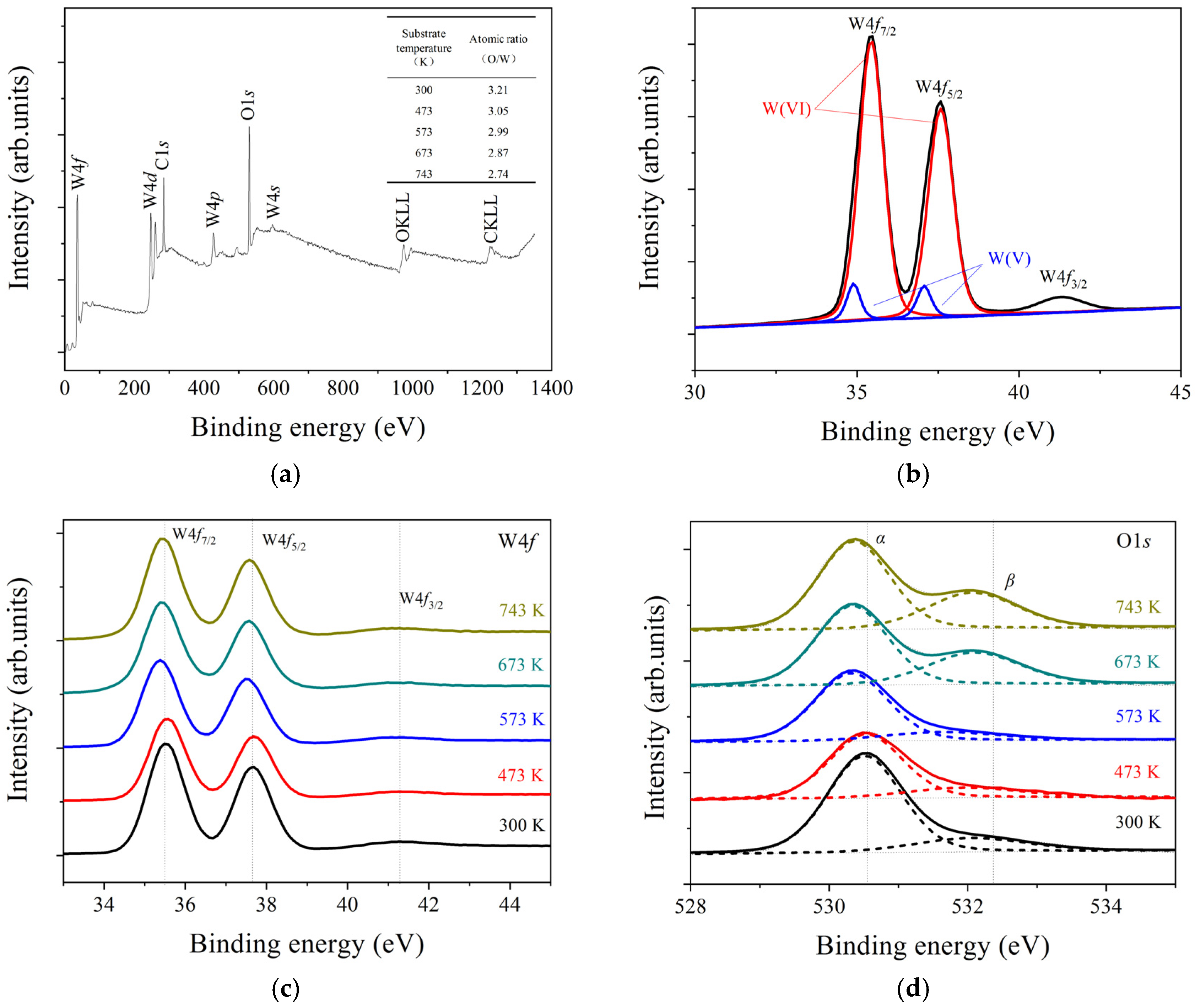
3.1. Structure and Composition

XRD was employed to determine the crystal structure and possible phase changes of WO3 thin films on different substrate temperatures, as the results are shown in Figure 1. It can be seen that there is no diffraction peaks for WO3 films at low substrate temperature of 300–473 K except for the peaks of ITO glass. The low intense peaks near 24° and 34° belonging to WO3 are observed at substrate temperature of 573 K, revealing the crystallinity transition. When the substrate temperature rises above 673 K, the positions of the reflection planes of WO3 film are 2θ = 23.1° (002), 2θ = 23.5° (020), and 2θ = 24.1° (200) corresponding to the monoclinic structure [JCPDS. 43-1035]. It can also be seen that the intensity of the Bragg reflection increases with the substrate temperature, indicating that the film has higher degree of crystallization at higher substrate temperature [20]. The results reveal that the crystal level of the WO3 can be controlled. The films deposited at 473 K are non-crystalline with amorphous properties. When increasing the temperature to 673 K, the (002), (020), and (200) diffraction appear indicating that the film grows into complete monoclinic phase crystals. Meanwhile, Scherrer formula was used to evaluate the microcrystalline size of the WO3 film, and the grain size was calculated to be approximately 12–28 nm. For the film deposited at 573 K, the wide and weak diffraction peaks at (002) and (400) indicate that the film is in a transition state between amorphous and nanocrystalline states [21].
XPS analysis was performed to investigate the chemical composition and reveal the elemental binding states of WO3 films. Figure 2a shows the full-scan XPS spectrum of WO3 films, mainly exhibiting W and O. It is calculated from the XPS element peak intensity that the atomic ratio W/O decreases with increasing substrate temperature may be related to the oxidation state of tungsten, because substrate temperature will affect the degree of reaction between the tungsten atoms and oxygen and influences the W and O combination of the film. Figure 2b shows the W4f spin-orbit energy level spectrum as a function of substrate temperature and the Gaussian fitted curve for film obtained at 573 K. There are continuous three spectrum corresponding to W4f7/2, W4f5/2, and W4f3/2 peaks which are located at 35.4, 37.7, and 41.3 eV, respectively, matching well with those reported in the literature for WO3 film [22]. The peaks at 35.4 and 37.7 eV were attributed to W4f7/2 and W4f5/2 for W(VI), whereas the peaks at 34.9 and 37.1 eV were attributed to W4f7/2 and W4f5/2 for W(V). Moreover, W4f7/2 and W4f5/2 can be split into W(VI) with higher binding energy and W(V) double peak with lower binding energy. However, the electrochromic process of WO3 film mainly realizes the mutual conversion between W(VI) and W(V), and absorbs the photon energy to undergo color conversion. Figure 2c shows that the peak position of the W4f spin trajectory shifts to the direction of low binding energy, and peak intensity also decreases as the substrate temperature increases. As a result, the ratio of W(VI)/W(V) in the obtained film is reduced, which restricts the process of film electrochromic from W(VI) to W(V), which affects its corresponding electrochromic performance. Figure 2d gives O1s spin orbit energy spectrum of the film at different substrate temperatures. The continuous double peaks represent the lattice oxygen (α) and the interstitial oxygen (β), respectively, corresponding to the binding energy of 530.7 and 532.0 eV. The relative content of the oxygen vacancy for WO3 films was evaluated according to the area ratio of these two integral components: (β peak)/(α peak + β peak), as the substrate temperature increased from 300 to 743 K, the surface oxygen vacancy content was 14.8%, 17.0%, 20.0%, 34.1% and 34.4%. As the substrate temperature increases oxygen vacancy concentration increases, indicating that the binding energy of the film is relatively low. In addition, the O1s binding energy also moved to a lower binding energy position, which accompany with phase transition of the film changed from amorphous to crystalline [23]. It can be known that as the substrate temperature increases, the peaks of W4f and O1s spin orbits move toward the lower binding energy, indicating lower chemical bond and more stable structure at higher substrate temperatures. The results show that the crystalline state has lower binding energy and more oxygen vacancy than the amorphous tungsten oxide.

3.2. Microscopic and Morphology

The prepared sample is an ITO and WO3 double layer film, in which the ITO as conductive layer and certain thickness of WO3 film is plated on the surface layer. The surface and cross-sectional SEM images of WO3 thin films at different substrate temperatures are illustrated in Figure 3. The literature reports that substrate temperature has a great influence on the growth of WO3 film [24]. When substrate temperature is 300 K, the film presents compact and smooth surface (Figure 3a). For the WO3 film prepared at 473 and 573 K, there is still a uniformly distributed spherical grain structure (Figure 3b,c). As the substrate temperature rises to 673 K, the spherical particles become islands and flakes (Figure 3d,e). At the same time, the crystalline state of the thin film changes, and the particle size of the thin film becomes small and flakes pile up. It also can be seen from the cross-sectional view that as the substrate temperature increases, the thin film growth leads to higher density. And the growth of the columnar crystal of the crystalline film becomes more obvious, which corresponds to the crystal orientation in the XRD pattern (200).
Furthermore, the surface roughness of WO3 film was characterized by AFM to analyze the film surface patterns grown at different substrate temperatures. The mean surface roughness (Rms) increases as a function of the substrate temperature as shown in Figure 4f. Due to the fact that as the substrate temperature increases, the deposited particles can obtain sufficient energy to migrate along the surface and inside, and combine with other particles to form crystals, and the crystal growth rate accelerates and the crystal grains become larger, resulting in an increase in surface roughness [25]. Figure 4a shows that the surface of the film is peak-shaped, and the roughness of amorphous WO3 thin film is approximately 2.43 nm. However, as the substrate temperature increases, the surface roughness becomes larger and the particle size becomes smaller. Since the electrochemical reaction first occurs on the surface of the film, the morphology may show important influence on the implantation and extraction of lithium ions, and therefore the effects observed in the current changes associated with the oxidation and reduction processes will be further discussed.

3.3. Optical Properties

Figure 5a shows the optical transmittance and absorbance of the WO3 films at different substrate temperatures in wavelength range of 300–800 nm. When comparing the transmittance of films at different substrate temperatures, the test deducts the ITO backing. The experiment keeps the thickness of the WO3 film within a certain range of 320–432nm, experimental tests confirm that the thickness has little effect on transmittance. The transmittance curve shows that as the substrate temperature increases, the interference wavelength of the transmittance of the WO3 film becomes larger, which means that the absorption coefficient of the film becomes smaller. The decrease in transmittance at higher substrate temperatures may be due to increase in surface roughness and improved crystallinity of the film resulting in more loss of light scattering. Generally, the sharp drop of transmittance was due to the fundamental absorption of light caused by the excitation of electrons from the valance band to the conduction band. It can be seen from the light absorption curve that the absorption edge moves to lower wavelength region as the substrate temperature increases, which called “blue shift” phenomenon [26]. It can be attributed to the presence of W(V) in the crystalline structure creating mid-gap defect states. Figure 5b shows the relationship between (αhν)2 and photon energy of the films formed at different substrate temperatures. When the substrate temperature is 473 K, the maximum optical band gap (Eg) of the film is 3.75 eV. The increased band gap can be attributed to more oxygen vacancy and enhanced crystallization of the film, making the refractive index of the film to light increase [27]. This is because it refracts light and increases the band gap of the film, high substrate temperature enhances regular arrangement of thin film, and the accompanying increased oxygen vacancy and crystalline regular structure will produce a high refractive index and absorption coefficient becomes smaller, resulting in a smaller optical band gap. Therefore, the width of the forbidden band increases with the substrate temperature, resulting in weakening the optical performance of the prepared WO3 film.

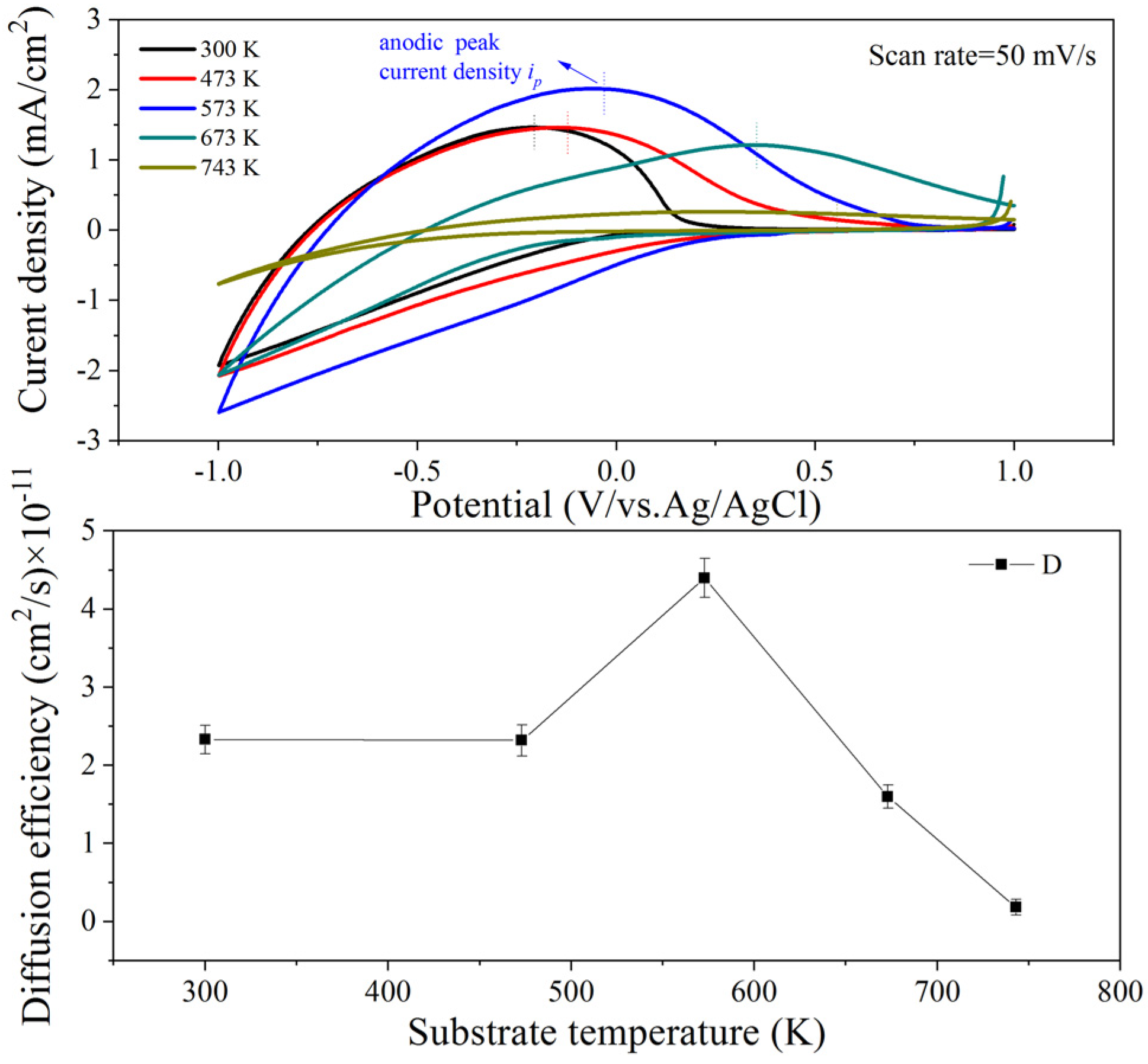
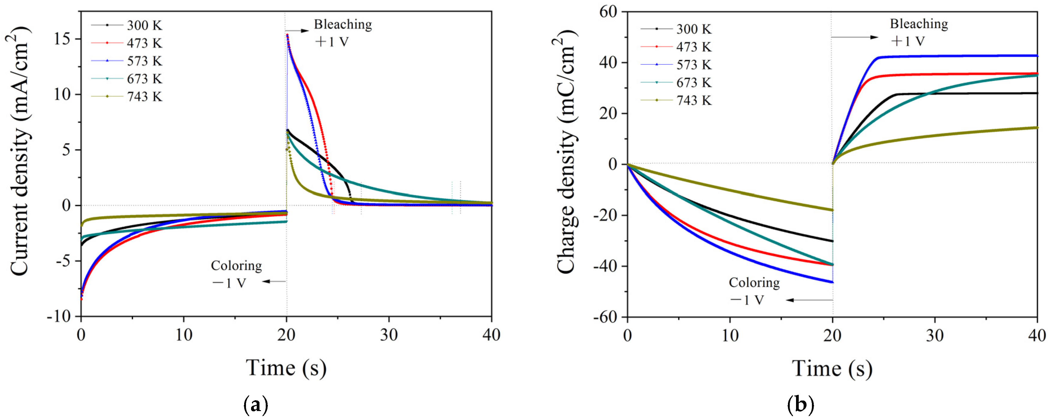
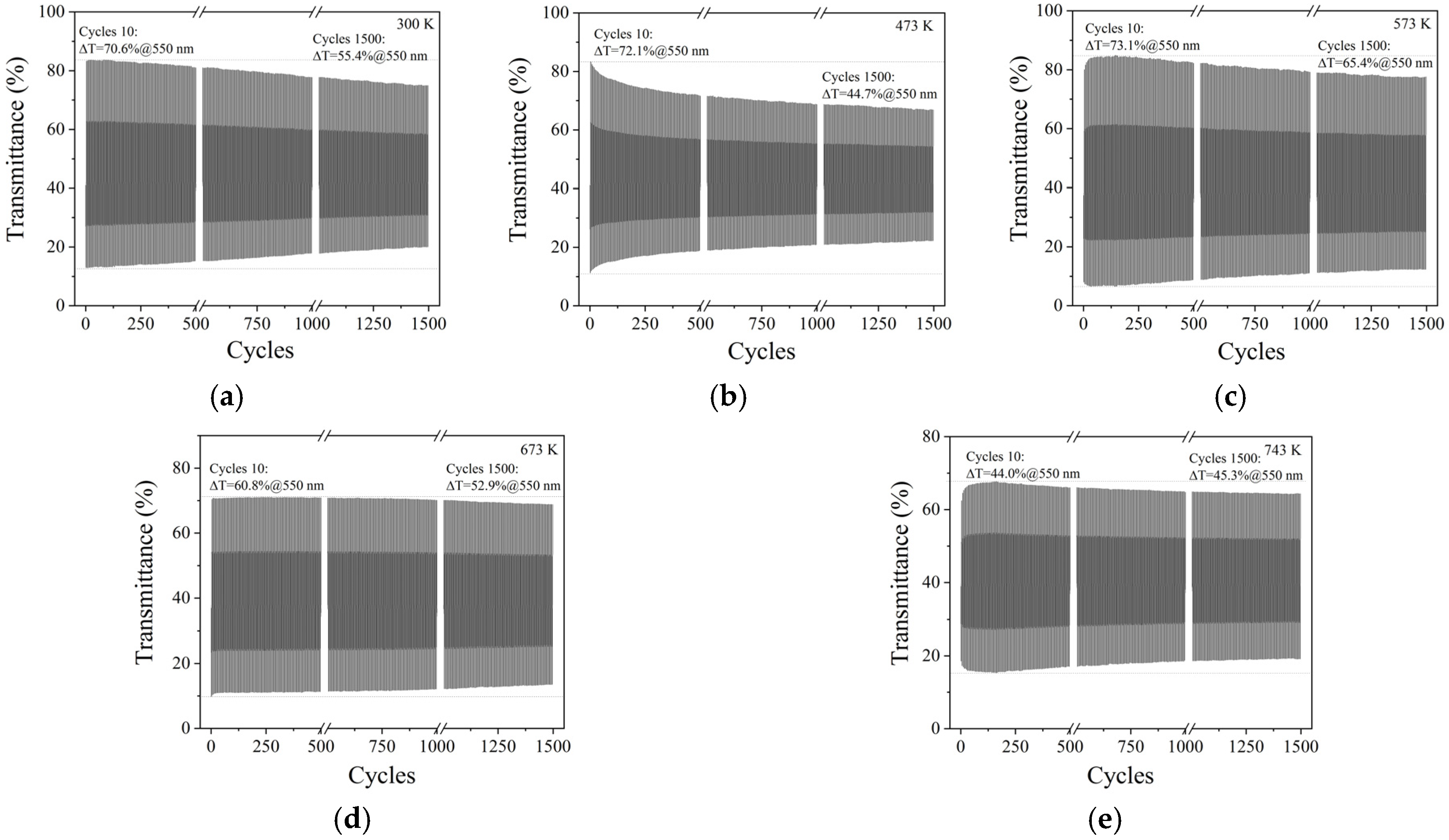
3.4. Electrochromic and Electrochemical Characterization

In order to investigate the electrochromic behavior of the films, the integrated area of the cyclic voltammetry curve and the position of the anode peak are calculated and identified, since they are closely related to the ion insertion/extraction and electrochemical process occurring in the electrochromic films. The principle of electrochromism is generally recognized by the double injection model of ions and electrons [28]. This process can be represented by the following reversible electrochemical reaction:
WO3 (transparent) + Li+ + e Coatings 10 00577 i001 LixWO3 (deep blue)
Typical cyclic voltammogram (CV) and lithium ion (Li+) diffusion efficiency for the WO3 film at different substrate temperatures are shown in Figure 6. It is considered that the larger integrated area of the CV curve, the more charge injected into the film, and the high anode peak position means greater Li+ diffusion efficiency. The Li+ diffusion coefficient (D) was determined according to the Randles–Sevcik equation [29]:
Ip = 2.72 × 10⁵ × D(1/2) × C0 × υ(1/2)
where Ip is the anodic peak current density, C0 the concentration of Li+ in the electrolyte, and ν the scan rate for CV test. As shown in Figure 6, when substrate temperature increases from 300 to 473 K the Ip increases, indicating the improved electrochemical characteristics. For the film prepared at 573 K, the CV integral curve area is the largest with the maximum anodic peak current density of 2.02 mA/cm2. After that, Ip sharply decreases. The calculated Li+ diffusion efficiency is shown in the inset of the Figure 6. According to the Randles–Sevcik equation, the maximum Li+ diffusion coefficient obtained at 573 K is 4.40 × 10⁻¹¹ cm2/s, it is superior to the previous Madhavi V. literature reports that the best diffusion efficiency of the prepared film ion is 1.85 × 10⁻¹¹ cm2/s. It can be attributed to the increased surface roughness and increased micro-void concentration of the film. When the substrate temperature is appropriately increased to 573 K, the loss structures between the amorphous and crystalline states can provide more effective contact area. The enhanced surface ion-implanting activity leads to an increase in the diffusion coefficient, which is in favor of lithium ion insertion/extraction [30]. However, the further substrate temperature increasing enhances the crystallinity and the formation of columnar crystal, which may cause a regular decrease in the Li+ diffusion coefficient.
The response time which is obtained by the trend of the current density change is a main evaluation indexes for electrochromic performance. The electrochemical test is performed by applying alternative ±1 V constant potentials, Figure 7 shows constant current step current density and charge density as a function of time. The calculated coloring time (tc) and bleaching time (tb) values are given in Table 1. When the substrate temperature is 300 K, the peak value of the response of tungsten oxide is 6.8 mA/cm2 and the maximum injection charge is −30.2 mC/cm2. For film prepared at higher substrate temperature, large charge density and a short fading time were detected. The maximum response current peak density obtained at 573 K is 15.3 mA/cm2, and the injected charge density is as high as −46.4 mC/cm2. After that, the degraded electrochromic properties with low response current density, small injection amount and long fading time were received at substrate temperature of 573–743 K. This trend is more pronounced with increases temperature, which should be attributed to their different microstructures especially the crystallinity. The WO3 films with amorphous structure provide more lithium ion diffusion channels and storage space, however the regularity and compaction crystal structure will weaken their corresponding electrochemical characteristics [31,32]. Figure 7 shows that the film obtained at substrate temperature of 573 K has a maximum substrate response current density and injected charge density, which is consistent with the CV results.
The detailed parameters for the electrochromic properties of tungsten oxide films prepared at different substrate temperatures are given in Table 1. The coloring efficiency (CE) in the wavelength range of 300–800 nm demonstrates the same regularity as the previously tested cyclic voltammetry (CV) and chronoamperometry (CA). As the temperature increases, the coloring efficiency first increases and then decreases. When the substrate temperature is 573 K, at 550 and 630 nm Wavelengths, the coloring efficiencies are maximum at 42.9 and 60.3 cm2/C, respectively. It is noticed that the decrease in coloring efficiency is accompanied with the increase of crystallinity degree. It is reported crystalline WO3 with O–W–O network interacts with lithium ions and forms a LixWO3 phase, which may reduce the coloration efficiency [33,34].
The durability is important for practical applications of WO3 films. It is known that crystal structures have important significance for the stability of electrochromic properties of WO3 thin films [35,36]. The above results show that the between amorphous and nanocrystalline state WO3 film with a substrate temperature of 573 K has a large modulation amplitude, a fast response speed, and a high coloring efficiency. It is necessary to analyze the cyclic stability of WO3 film under different substrate temperatures. Figure 8 shows the transmittance variation for the WO3 thin film after 1500 cycles at different substrate temperatures, there is obvious cyclic degradation for the film with amorphous structure modulation amplitude retention rate of 89.5% after 1500 cycles, indicating the excellent cycle stability at substrate temperature under 573 K, however crystalline films can provide stable cycling performance. This is due to the low binding energy of the crystalline WO3 film, which is more regular and stable, and has a distinct columnar structure and crystal orientation. During the WO3 thin film is periodically colored process, the columnar and orientation crystal can provide shorter migration distance for lithium ions [37,38]. It is noticed that although the attenuation of the amorphous WO3 film is even worse after 1500 cycles, it still has better color rendering ability than the crystal one. In general, for the film deposited at 573 K has the best electrochromic properties including the shortest response time, the largest optical modulation and the most stability. This is because the film with combined nanocrystalline and amorphous structure can provide more sites and short diffusion path for lithium ion injection/extraction.

4. Conclusions

In this study, DC reactive magnetron sputtering method was used to deposit WO3 film on the ITO substrate, and the microstructure and crystal structure were adjusted by changing the substrate temperature. The results show with substrate temperature increasing from 300 to 743 K, the WO3 thin film changes from amorphous to monoclinic phase crystal state. Unexpectedly, when the substrate temperature is 573 K, the WO3 films have a combined structure of amorphous and nanocrystalline. XPS measurement confirms that as the substrate temperature increases, the ratio of W(VI)/W(V) decreases, oxygen vacancies increase, and the binding energy of the thin film changes to a regular crystal structure. The electrochromic properties of the deposited WO3 films were first improved and then degraded with the increase of substrate temperature. The WO3 films deposited at substrate temperature of 573 K with Li+ diffusion coefficient of 4.40 × 10⁻¹¹ cm2/s, demonstrate the best optical modulation of 73.1% and coloration efficiency of 49.2 cm2/C at a wavelength of 550 nm. And the modulation amplitude retention rate of 89.5% after 1500 cycles is achieved, indicating the excellent cycle stability. These results indicate that changing the substrate temperature can effectively improve the electrochromic properties of the WO3 film. This should attribute to the intermediate states between amorphous and nanocrystalline, which can provide more sites and short diffusion path for lithium ion injection/extraction.

Author Contributions

Conceptualization, H.-l.W.; methodology, Z.-j.X.; formal analysis, Q.S. and Z.-g.Z.; investigation, Y.-f.S. and H.-j.L.; writing—original draft preparation, Z.-j.X.; writing—review and editing, P.T.; supervision, M.-j.D. All authors have read and agreed to the published version of the manuscript.

Funding

This research was funded by Guangdong Special Support Program (No. 2019BT02C629), Scientific Research Fund of Guangdong Province (2016A030312015), GDAS’Project of Science Technology Development (No. 2018 GDASCX-0402), GDAS’ Talent Introduction Project (No. 2020GDASYL-20200103110).

Conflicts of Interest

The authors declare no conflict of interest.

References

  1. Deb, S.K. A novel electrophotographic system. Appl. Opt. 1969, 8, 192–195. [Google Scholar] [CrossRef]
  2. Niklasson, G.A.; Granqvist, C.G. Electrochromics for smart windows: Thin films of tungsten oxide and nickel oxide, and devices based on these. J. Mater. Chem. A 2007, 17, 127–156. [Google Scholar] [CrossRef] [Green Version]
  3. Granqvist, C.G. Electrochromics for smart windows: Oxide-based thin films and devices. Thin Solid Films 2014, 564, 1–38. [Google Scholar] [CrossRef]
  4. Chang, J.Y.; Chen, Y.C.; Wang, C.M.; Wang, W.N.; Wen, C.Y.; Lin, J.M. Electrochromic properties of Lithium-doped tungsten oxide prepared by electron beam evaporation. Coatings 2019, 9, 191. [Google Scholar] [CrossRef] [Green Version]
  5. Kim, K.H.; Koo, B.R.; Ahn, H.J. Title of the chapter Sheet resistance dependence of fluorine-doped tin oxide films for high-performance electrochromic devices. Ceram. Int. 2018, 44, 9408–9413. [Google Scholar] [CrossRef]
  6. Jiang, B.; Lou, B.; Li, J.; Peng, P.; Chen, J.W.; Chu, L.H.; Li, Y.F.; Li, M.C. Electrochemical effect of graphite fluoride modification on Li-rich cathode material in lithium ion battery. Ceram. Int. 2019, 45, 160–167. [Google Scholar] [CrossRef]
  7. Liu, R.; Zheng, Z.; Spurgeon, J.; Yang, X.G. Enhanced photoelectrochemical water-splitting performance of semiconductors by surface passivation layers. Energy Environ. 2014, 7, 2504–2517. [Google Scholar] [CrossRef] [Green Version]
  8. Kim, K.H.; Koo, B.R.; Ahn, H.J. Effect of Sb-doped SnO2-WO3 nanocomposite on electrochromic performance. Ceram. Int. 2019, 45, 15990–15995. [Google Scholar] [CrossRef]
  9. Pan, J.B.; Wang, Y.; Zheng, R.Z.; Wang, M.T.; Wan, Z.Q.; Jia, C.Y.; Weng, X.L.; Xie, J.L.; Deng, L.J. Directly grown high-performance WO3 films by a novel one-step hydrothermal method with significantly improved stability for electrochromic applications. J. Mater. Chem. A 2019, 7, 13956–13967. [Google Scholar] [CrossRef]
  10. Hua, C.Z.; Yuan, G.Z.; Cheng, Z.Q.; Jiang, H.; Xu, G.; Liu, Y.; Han, G.R. Building architecture of TiO2 nanocrystals embedded in amorphous WO3 films with improved electrochromic properties. Electrochim. Acta 2019, 309, 354–361. [Google Scholar] [CrossRef]
  11. Zheng, H.D.; Ou, J.Z.; Strano, M.S.; Kaner, R.B.; Mitchell, A.; Kalantar-Zadeh, K. Nanostructured tungsten oxide-properties, synthesis, and applications. Adv. Funct. Mater. 2011, 21, 2175–2196. [Google Scholar] [CrossRef]
  12. Dong, P.Y.; Hou, G.H.; Xi, X.U.; Shao, R.; Dong, F. WO3-based photocatalysts: Morphology control, activity enhancement and multifunctional applications. Environ. Sci. Nano 2017, 4, 539–557. [Google Scholar] [CrossRef]
  13. Valyukh, I.; Green, S.V.; Granqvist, C.G.; Niklasson, G.A.; Valyukh, S.; Arwin, H. Optical properties of thin films of mixed Ni-W oxide made by reactive DC magnetron sputtering. Thin Solid Films 2011, 519, 2914–2918. [Google Scholar] [CrossRef] [Green Version]
  14. Stanishevsky, A.V.; Wetuski, J.D.; Yockell-Lelievre, H. Crystallization and stability of electrospun ribbon- and cylinder-shaped tungsten oxide nanofibers. Ceram. Int. 2016, 42, 388–395. [Google Scholar] [CrossRef]
  15. Nunez, O.R.; Tarango, A.J.M.; Murphy, N.R.; Phinney, L.C.; Hossain, K.; Ramana, C.V. Physical characterization of sputter-deposited amorphous tungsten oxynitride thin films. Thin Solid Films 2015, 596, 160–166. [Google Scholar] [CrossRef] [Green Version]
  16. Zhang, H.J.; Chen, C.H.; Bahnemann, D.W. Photoelectrocatalytic materials for environmental applications. J. Mater. Chem. 2009, 19, 5089–5121. [Google Scholar] [CrossRef]
  17. Gaurav, M.; Satyendra, M.; Jignesh, G.H.; Ramesh, G. Surface modification of sputter deposited γ-WO3 thin film for scaled electrochromic behaviour. Surf. Coat. Technol. 2019, 375, 708–714. [Google Scholar]
  18. Madhavi, V.; Kondaiah, P.; Hussain, O.M.; Uthanna, S. Structural, optical and electrochromic properties of RF magnetron sputtered WO3 thin films. Physica B 2014, 454, 141–147. [Google Scholar] [CrossRef]
  19. Mong, D.M.; Wang, W.W.; Dong, G.B.; Zhang, F.; He, Y.C.; Yu, H.; Liu, F.M.; Wang, M.; Xiao, X.G. Electrochromic properties and performance of NiOx films and their corresponding all-thin-film flexible devices preparedby reactive DC magnetron sputtering. Appl. Surf. Sci. 2016, 383, 49–56. [Google Scholar]
  20. Liang, Y.C.; Chang, C.W. Preparation of orthorhombic WO3 thin films and their crystal quality-dependent dye photodegradation ability. Coatings 2019, 9, 90. [Google Scholar] [CrossRef] [Green Version]
  21. Zheng, F.; Man, W.K.; Guo, M.; Zhang, M.; Zhen, Q. Effects of morphology, size and crystallinity on the electrochromic properties of nanostructured WO3 films. CrystEngComm 2015, 17, 5440–5450. [Google Scholar] [CrossRef]
  22. Niklasson, G.A.; Berggren, L.; Larsson, A.L. Electrochromic tungsten oxide: The role of defects. Sol. Energy Mater. Sol. C 2004, 84, 315–328. [Google Scholar] [CrossRef]
  23. Kim, H.; Choi, D.; Kim, K.; Chu, W.; Chun, D.M.; Lee, C.S. Effect of particle size and amorphous phase on the electrochromic properties of kinetically deposited WO3 films. Sol. Energy Mater. Sol. C 2018, 177, 44–50. [Google Scholar] [CrossRef]
  24. Kawar, R.K.; Chigare, P.S.; Patil, P.S. Substrate temperature dependent structural, optical and electrical properties of spray deposited iridium oxide thin films. Appl. Surf. Sci. 2003, 206, 90–101. [Google Scholar] [CrossRef]
  25. Xu, X.L.; Yazdi, M.A.P.; Rauch, J.Y.; Salut, R.; Bilard, A.; Potin, V.; Martin, N. Tungsten oxide thin films sputter deposited by the reactive gas pulsing process for the dodecane detection. Mater. Today Proc 2015, 2, 4656–4663. [Google Scholar] [CrossRef]
  26. Subrahmanyam, A.; Karuppasamy, A. Optical and electrochromic properties of oxygen sputtered tungsten oxide (WO3) thin films. Sol. Energy Mater. Sol. C 2007, 91, 266–274. [Google Scholar] [CrossRef]
  27. Sun, X.L.; Liu, Z.M.; Cao, H.T. Electrochromic properties of N-doped tungsten oxide thin films prepared by reactive DC-pulsed sputtering. Thin Solid Films 2011, 519, 3032–3036. [Google Scholar] [CrossRef]
  28. Ghosh, K.; Roy, A.; Tripathi, S.; Ghule, S.; Singh, A.K.; Ravishankar, N. Insights into nucleation, growth and phase selection of WO3: Morphology control and electrochromic properties. J. Mater. Chem. A 2017, 5, 7307–7316. [Google Scholar] [CrossRef]
  29. Leftheriotis, G.; Papaefthimiou, S.; Yianoulis, P. Dependence of the estimated diffusion coefficient of LixWO3 films on the scan rate of cyclic voltammetry experiments. Solid State Ion. 2007, 178, 259–263. [Google Scholar] [CrossRef]
  30. Wen, R.T.; Granqvist, C.G.; Niklasson, G.A. Eliminating degradation and uncovering ion-trapping dynamics in electrochromic WO3 thin films. Nat. Mater. 2015, 14, 996–1001. [Google Scholar] [CrossRef] [Green Version]
  31. Babu, M.B.; Madhuri, K.V. Synthesis and electrochromic properties of nanocrystalline WO3 thin films. Physica B 2020, 584, 68–75. [Google Scholar] [CrossRef]
  32. Martin, L.W.; Chu, Y.H.; Ramesh, R. Advances in the growth and characterization of magnetic, ferroelectric, and multiferroic oxide thin films. Mater. Sci. Eng. R 2010, 68, 111–133. [Google Scholar] [CrossRef] [Green Version]
  33. Kharade, R.R.; Mali, S.S.; Patil, S.P.; Patil, K.R.; Gang, M.G.; Patil, P.S.; Kim, J.H.; Bhosale, P.N. Enhanced electrochromic coloration in Ag nanoparticle decorated WO3 thin films. Electrochim. Acta 2013, 102, 358–368. [Google Scholar] [CrossRef]
  34. Rauh, R.D.; Wang, F.; Reynolds, J.R.; Meeker, D.L. High coloration efficiency electrochromics and their application to multi-color devices. Electrochim. Acta 2001, 46, 13–14. [Google Scholar] [CrossRef]
  35. Zelays-Angel, O. Electrocoloration curve analysis in WO3 thin films. Mater. Sci. Eng. B Solid 2001, 86, 123–127. [Google Scholar] [CrossRef]
  36. Nagai, J.; Mcmeeking, G.D.; Saitoh, Y. Durability of electrochromic glazing. Sol. Energy Mater. Sol. C 1999, 56, 309–319. [Google Scholar] [CrossRef]
  37. Cai, G.F.; Darmawan, P.; Cui, M.Q.; Wang, J.X.; Chen, J.W.; Magdassi, S.; Lee, P.S. Highly stable transparent conductive silver grid/PEDOT: PSS electrodes for integrated bifunctional flexible electrochromic supercapacitors. Adv. Energy Mater. 2016, 6, 2–8. [Google Scholar] [CrossRef]
  38. Sallard, S.; Brezesinski, T.; Smarsly, B.M. Electrochromic stability of WO3 thin films with nanometer-scale periodicity and varying degrees of crystallinity. J. Phys. Chem. C 2007, 111, 7200–7206. [Google Scholar] [CrossRef]
Figure 1. X-ray diffraction (XRD) patterns of the WO3 thin films deposited at different substrate temperature.
Coatings 10 00577 g001
Figure 2. The WO3 thin films deposited at different substrate temperatures: (a) X-ray photoelectron spectroscopy (XPS) full spectra, (b) W4f Gaussian fitting peak spectra, (c) W4f spin orbit energy level spectra and (d) O1s spin orbit energy level spectra.
Coatings 10 00577 g002
Figure 3. Surface and cross section scanning electron microscope (SEM) images of WO3 thin films deposited at different substrate temperatures (a) 300 K, (b) 473 K, (c) 573 K, (d) 673 K and (e) 743 K.
Coatings 10 00577 g003
Figure 4. Surface atomic force microscope (AFM) images of WO3 thin films deposited at different substrate temperatures (a) 300 K, (b) 473 K, (c) 573 K, (d) 673 K, (e) 743 K and (f) Ra curve.
Coatings 10 00577 g004aCoatings 10 00577 g004b
Figure 5. The WO3 films deposited at different substrate temperature: (a) transmittance and absorption coefficient curve and (b) Tuac plot and Eg curve.
Coatings 10 00577 g005
Figure 6. Cyclic voltammetry (CV) and diffusion efficiency curve of WO3 films deposited at different substrate temperatures.
Coatings 10 00577 g006
Figure 7. The WO3 films deposited at different substrate temperatures: (a) chronoamperometry (CA) and (b) chronocoulometry (CC) curves.
Coatings 10 00577 g007
Figure 8. The transmistance curve of WO3 film after 1500 cycles deposited at different substrate temperatures: (a) 300 K, (b) 473 K, (c) 573 K, (d) 673 K and (e) 743 K.
Coatings 10 00577 g008
Table 1. Electrochromic index various parameter of WO3 films deposited at different substrate temperatures.
Substrate Temperatures (K)Optical Modulation Range (%)Response Time (s)Coloration Efficiency (cm2/C)
550 nm630 nmtbtc550 nm630 nm
30070.675.36.313.532.947.4
47372.178.44.411.037.952.4
57373.179.93.910.542.960.3
67360.867.714.415.525.943.2
74344.056.616.417.219.838.3

