
Research Progress of Biomimetic Memristor Flexible Synapse
by
 , , and
Huiling Zhang
1,†, 
Ruping Liu
1,†,
Huiqing Zhao
1,
Zhicheng Sun
1,
Zilong Liu
2,
Liang He
3 and
Ye Li
1,* 1
Beijing Institute of Graphic Communication, Beijing 102600, China
2
Division of Optics, National Institute of Metrology, Beijing 100029, China
3
School of Mechanical Engineering, Sichuan University, Chengdu 610065, China
*
Author to whom correspondence should be addressed.
†
These authors contributed equally to this work.
Coatings 2022, 12(1), 21; https://doi.org/10.3390/coatings12010021
Submission received: 7 August 2021
/
Revised: 7 November 2021
/
Accepted: 16 November 2021
/
Published: 25 December 2021
(This article belongs to the Special Issue Thin Films for Electronic Devices)
Abstract
:With the development of the Internet of things, artificial intelligence, and wearable devices, massive amounts of data are generated and need to be processed. High standards are required to store and analyze this information. In the face of the explosive growth of information, the memory used in data storage and processing faces great challenges. Among many types of memories, memristors have received extensive attentions due to their low energy consumption, strong tolerance, simple structure, and strong miniaturization. However, they still face many problems, especially in the application of artificial bionic synapses, which call for higher requirements in the mechanical properties of the device. The progress of integrated circuit and micro-processing manufacturing technology has greatly promoted development of the flexible memristor. The use of a flexible memristor to simulate nerve synapses will provide new methods for neural network computing and bionic sensing systems. In this paper, the materials and structure of the flexible memristor are summarized and discussed, and the latest configuration and new materials are described. In addition, this paper will focus on its application in artificial bionic synapses and discuss the challenges and development direction of flexible memristors from this perspective.
1. Introduction
According to circuit theory, any two of the circuit variables voltage (v), charge (q), current (i), and magnetic flux (Φ) have a certain relationship, that is, voltage/current = resistance, charge/voltage = capacitance, magnetic flux/current = inductance, but there is no circuit element associating charge with magnetic flux. Around the year 1800, the University of California discovered memristive switching behavior [1]. Until 1971, Cai studied the relationship between the four basic circuit variables of voltage, current, charge and magnetic flux (Figure 1). Based on the principle of complete circuit combination and physical symmetry, he believed that in addition to resistance, capacitance, and inductance, there should be an element (missing element) that represents the relationship between electric charge and magnetic flux, and he named the circuit element “memristor” [2,3]. In 2008, researchers prepared the first working memristor with a metal/oxide/metal sandwich structure based on TiO2 and measured its electrical properties as well as obtained the “8” shape of the device [4]. After analyzing the volt-ampere characteristic curve, they finally determined that the device whose resistance can be changed by the externally controllable operating voltage and current is the memristor [4]. Since then, researchers in various fields have continued to invest in it, and memristors made of various new materials, such as inorganic materials and two-dimensional materials, and innovative structures have been continuously studied, and their working mechanisms have been continuously explored.
Under the stimulation of voltage or current, the memristor will be switched between high and low resistances, corresponding to the two states of “0” and “1” in the computer to store data. At present, the memristor has a simple structure, good scalability (<10 nm), high-density storage, low power consumption (<0.1 pJ), ultra-fast operating speed (sub-ns), high durability (>1012 switching cycles), and other advantages. It has become an important next-generation storage technology [5,6,7,8,9,10].
The electrical characteristics of the memristor match the transmission working principle of the nerve synapse. The pre-synapse and post-synapse correspond to the top and bottom electrodes of the memristor, and the synaptic cleft corresponds to the dielectric layer (Figure 2). The memristor can simulate the nerve synapse’s working process, such as discharge time, which depends on plasticity (STDP) [11], long/short-term synaptic plasticity (STP/LTP) [12], and joint memory [13]. In addition, the memristor can be used to create a neural network chip to perform certain functions, such as perception calculations [14]. These functions are realized by the interconnection of about 1011 neurons and 1015 synapses in the human brain. The connection mode and strength are affected by the level of memory and information processing [15]. The traditional integrated chip simulation has the bottleneck problem of von Neumann architecture [16]. Adopting memristors by imitating the structure and working mechanism of biological synapses and the information processing methods of the human brain to develop neural network-like calculations has natural advantages in terms of reliability, scalability, and fault tolerance, which is a potential way to achieve efficient calculations.
In addition, the rapid development of electronic information technology has attracted more and more attention to functional electronic devices. Medical health monitoring has an urgent need for flexible, wearable electronic devices. To ensure that the entire electronic system has excellent flexibility, the memristor, as the key component, will also develop in the direction of flexibility [17]. Furthermore, the memristor shows great advantages and potential in terms of flexibility, which can meet the requirements for miniaturization, high density, high durability, and low energy consumption. In the future, they will become an important part of wearable electronic devices and artificial nerve synaptic bionic devices.
In this review, we introduce the latest development in the research of flexible memristors, focusing on summarizing the important basic functions and innovative research results. This review mainly elaborates on these three aspects: (1) the flexible memristor materials, including electrode materials, dielectric layer materials (metal oxides, two-dimensional materials, biodegradable materials, etc.), and substrate materials; (2) the structures of the flexible memristor, including traditional sandwich structures, planar structures, and new derivative structures, etc.; (3) based on the application of flexible memristors, focusing on the application of artificial bionic synapses at both ends, and introducing their research in simulating synaptic plasticity, including STDP, LTP, STP, and memory formation, etc. In addition, we summarized the calculation and work of the artificial synaptic neural network for the memristor and analyzed the problems it faces and future development.
2. Flexible Memristor Material
The memristor is composed of the upper and lower electrode layers, the intermediate dielectric layer, and the substrate. Different materials have a crucial influence on the performance of the memristor. This chapter will review the common materials and new types of the various components of the flexible memristor material.
2.1. Flexible Electrode Material
The electrode material of the memristor must not only have the function of conducting current but must also participate in the resistance change reaction [18,19,20]. The electronic barrier at the electrode/dielectric interface is formed by the presence of high concentrations of interface states [21]. Therefore, the interfacial states greatly determine the resistance values and switching properties of the device. Currently, commonly used electrode materials include metals (Al, Mg, Au, and Ag), oxides (ITO), nitrides (AlN), and silicon-based materials [18,21]. Among electrode materials, due to their excellent mechanical properties, metals and oxides are promising flexible memristor electrode materials.
Some of these metal materials have high conductivity and flexibility, such as Ti [22], Mg [23], Ag [24], and W [25]. These materials are used in the preparation of flexible memristors. Nagareddy et al. [26] used Ti and Pt as the electrodes to prepare a high-performance memristor, with a size of 50 nm, an operating speed of less than 5 ns, and a thickness of 8 nm. Even after bending 5000 times under a radius of 9 mm, there was almost no obvious degradation in the device performance. When the bending radius was reduced to 6 mm (considered as “extreme bending”), the high-to-low resistance ratio of the device remains unchanged. With continued further bends to 4 and 2 mm (almost folded in half), due to electrode fracture, the device fails. The device showed excellent durability and mechanical flexibility. Andrey et al. [27] used Pt as the electrode material and prepared Ti/TaOx/IGZO/Pt flexible memristor switches. As the bending curvature increased, the device showed a slight reduction in the synaptic memory window. When the bending curvature Ø < ~10mm, the “cracks” appeared in TaOx/IGZO thin films. However, Young’s moduli of Ti, Pt, TaOx, and IZGO thin films are ~110, ~170, ~120, and ~129 GPa, respectively. Because of the elasticity of Pt, the device can work normally even after the cracks are formed in the TaOx/IGZO film.
In order to meet the requirements of some wearable devices, the prepared memristor must be both flexible and transparent. Therefore, many transparent materials have also been applied to the electrodes of the memristor, such as indium tin oxide (ITO) [28], ZnO [29], etc. Shang et al. [30] prepared a flexible, transparent ITO/HfOx/ITO/PET memristor with excellent optical and mechanical properties. It is observed that the device has a high optical transmittance exceeding 80% and low dispersion. The dispersion coefficient is less than 12.8%. In addition, the device can withstand up to 2.12% mechanical tensile stress. When the bending radius is not less than 5 mm (bending strain is not more than 1.27%), the device can undergo 1200 bending fatigue tests, and the resistance transformation performance is almost unaffected. Zhou et al. [31] designed a multi-color, light-modulated, transparent ITO/BP@PS/ITO memristor based on black phosphorous (BP), showing a transmittance of >75% between 350 and 1100 nm. The memristor’s performance is improved by light in the ultraviolet (380 nm) and near-infrared (785 nm) range, the power consumption and reset voltage are decreased, and the on/off ratio is increased 10 fold. It has great potential in wearable and transparent electronic devices.
ZnO not only has the characteristics of flexibility and transparency but also has optoelectronic properties comparable to traditional ITO films. It is also rich in raw materials, low in price, nontoxic, and high in thermal stability. Mundle et al. [29] used an atomic layer deposition and obtained the ZnO and an Al: ZnO layer on a ZnO-based substrate, prepared a ZnO/Al:ZnO transparent memristor switch, and demonstrated it under different light sources which has good switching performance.
Doping Al in the ZnO system can produce ZnO: Al transparent conductive film, i.e., AZO film. After doping, the conductivity of the film is greatly improved. Le et al. [32] designed the AZO/NiO/AZO/muscovite (ANA/muscovite) transparent flexible memristor structure (Figure 3). The memristor meets all the most stringent requirements of transparent soft devices; it has more than 80% optical transparency, a high performance under visible light, an on/off resistance ratio >105, high durability of 103 cycles, and a long retention time of 105 s. Additionally, the ANA/muscovite memristor can work under various bending radii below 5 mm and can mechanically bend with a radius of curvature of 6.5 mm and a high temperature of up to 185 °C after 1000 cycles, which have future applications. This research marks an important milestone in the progress of transparent, flexible, and nonvolatile electronic technology for next-generation, smart wearable devices.
Moreover, the transparent memristor is more conducive to the observation principle. Qian et al. [33] proposed an ITO/hBN/graphene/PDMS memory device with high transmittance (~85%) over the visible region and excellent stability at bending conditions. What’s more, they directly observed indium filaments in the device via ex-situ transmission electron microscopy [33].
2.2. Flexible Dielectric Layer Material
The electrochemical performance and working mechanism of memristors largely depend on the material of the dielectric layer. In order to obtain a memristor with excellent performance, various materials have been applied to it, such as metal oxides [34], organic polymers, two-dimensional materials [35], and biodegradable materials [36].
2.2.1. Metal Oxide Flexible Memristor
Compared with other materials, the flexible memristor with oxide as the dielectric layer has a simple structure, and the material composition is easy to control. Metal oxides used in memristors mainly include TiO2, NiO, HfO2, etc.
However, most transition metal oxide films are naturally rigid, so they require special treatment before application in flexible electronic devices. Son et al. [37] designed the TiO2 dielectric layer to be serpentine (~66 nm) and deposited it on the Al electrode using magnetron sputtering. In the case of stretching to 25%, the stress induced at the junction of the TiO2 dielectric layer and the two electrodes is lower than 0.1% and 0.05%, respectively, so that damage is not caused to the device structure and performance degradation. Even after 1000 stretching cycles (30% strain), the device can still maintain stable electrical properties.
With an excellent dielectric constant (~25) and Young’s modulus (~74.3 GPa) [20,21], HfO2 exhibits satisfactory switching performance and will provide potential applications in flexible electronic devices [38]. Zhang et al. [38] prepared an ITO/HfO2/TiN/polyimide access memory (memristor) device that used HfO2 as a dielectric layer. This flexible device showed stable resistance characteristics at different bending radii up to 4 mm, and after bending the device 1000 times, it showed more than 1.5 × 10⁵ write/erase cycles.
In metal-oxide based memristors, the formation and fracture of conductive filaments cause impedance changes during the switching cycle. The bending and stretching of the memristor will affect the formation and fracture of conductive filaments. Doping ions in metal oxide is an effective way to solve the problem [39]. Paul et al. [40] dopped Al in HfOx as a dielectric layer and fabricated a flexible Al/Al-doped HfOx/ITO/PET resistive memory device, and it showed excellent switching performance, such as resistance ratio (>103) and retention (104 s). They also investigated the applications of the 7.5% Al-doped HfOx device. The memory window slightly decreases as the bending radius starts from the flat condition (20 mm) to the bending condition (5 mm). This should be due to cracks in the bottom electrode of ITO at extreme bending conditions.
The TiO2/HfO2 double-layer structure shows excellent characteristics, such as multiple resistance states, self-rectification, self-compliance, and stable bipolar electrical impedance characteristics, while being flexible [41]. Compared with Ti/TiO2/Si devices, Ti/TiO2/HfO2/Si devices exhibit nonlinearity and high rectification current–voltage characteristics [42]. Zhang et al. [43] prepared a flexible memristor with a double-layer TiO2/HfO2 structure on a polyethylene naphthalate (PEN) substrate, which showed excellent uniformity, excellent mechanical flexibility, and high durability. Under mechanical stress with a bending radius of 10-70 mm, no performance degradation was observed. Interestingly, the performance degradation after long-term stability testing can be recovered. The asymmetric, hourglass-shaped, oxygen vacancy distribution on the hafnium dioxide/titanium dioxide interface has a key role in the performance of this flexible memristor device.
Adding a buffer layer between electrode and dielectric layer is also a way to improve the flexibility of the memristor. In addition, it can also improve the adhesion between them and improve the memristor switching characteristics. Kumar et al. [44] used Al2O3 buffer layers on both sides of the ZnO, which help stabilize the local oxygen migration of conductive filament formation and rupture during continuous switching cycles, and studied a bipolar resistive switch memristor with TiN/Al2O3/ZnO/Al2O3/TiN structure and flexible, non-volatile memory applications. It showed uniform and very stable bipolar resistance switching characteristics. Its resistance on-off ratio is two orders of magnitude higher, maintained at 120 °C for more than 104 s, and its durability is more than 108 cycles without any degradation. In addition, when under 104 consecutive repeated flexible bends (bending radius of up to 3 mm), the device showed high mechanical stability and high durability. Fang et al. [45] inserted MgO as an intermediate layer between MoO3 layers to improve device performance and prepared a high-performance, biodegradable, transient, resistance random access memory with a Mg/MoO3/MgO/MoO3/Mg structure on a polylactic acid substrate.
2.2.2. Organic Polymers Flexible Memristor
There has been some scientific research on memristors in recent years, and the mechanism of inorganic memristors is relatively clear, but there are still some shortcomings. Inorganic devices are rigid, fragile, and incompatible with biological tissues, which greatly restrict their applications in wearable devices. In addition, the materials produced in the process of preparing the metal oxide memristor pollute the environment. In contrast, organic materials with good flexibility, biocompatibility, and low-cost preparation, have a greater potential in the preparation of flexible and stretchable high-performance memristors [46].
So far, many organic materials have been reported to have resistance transition properties and have been used in flexible resistive random access memory, including inorganic materials, polymers, and their composite materials, which generally exhibit better mechanical flexibility. Wang et al. [47] designed a highly transparent, flexible, biocompatible, PEDOT: PSS-based memristor (Al/PEDOT: PSS/ITO). After 1000 folding destructive experiments, the synaptic weight enhancement/inhibition behavior of the memristive device was tested and it was found that it can still simulate 10 long-term enhancement/inhibition cycles, indicating that the device has good flexibility. The manufacturing process is low-cost, facile, and compatible with flexible substrates which can be performed at a temperature lower than 120 °C. Jang et al. [48] fabricated a poly (1,3,5-trivinyl-1,3,5-trimethyl cyclotrisiloxane) (pV3D3)-based flexible memristor (Figure 4). Due to the inherent flexibility of pV3D3 film, even under mechanical deformation, the pV3D3 memristor with a copper top electrode and an aluminum bottom electrode works in a binary switch mode through the formation and fracture of the copper wire.
Solution processing manufacturing methods including spin-coating, are low-cost, facile, and scalable, so they are suitable for large-scale, industry-standard coatings. Therefore, there is a lot of room for the development of flexible and low-cost transient storage devices using facile and easy solution processing and manufacturing technologies, such as spin coating biodegradable composite transient materials [49,50]. However, resistance switching is determined by the formation and fracture of metallic conductive wires (CFs). The overall injection of metal ions in the electrolyte and any ion migration in the electrolyte leads to the random formation of CFs, which inevitably involves low uniformity and poor reliability of the device [51]. Besides, the organic film produced by a typical solution process is thicker than the inorganic film, which reduces the flexibility, and the organic memristor requires higher power [52]. Park et al. [53] introduced an interface load layer (PMMA) into the device and demonstrated a solution-processed organic memristor with high reliability, high uniformity, and low operating current. At the bending radius of up to 5 mm, mechanically deformed devices continue to work as stable bipolar memories. During the repeated cycles of bending and relaxation of rb = 5 mm, the current level of the device at LRS and HRS states remained good, and there was no degradation in 2.8 × 10³ s.
Compared with the traditional device without ILP, the flexible memristor with ILP works stably at repeated bending-straightening deformation and provides higher electrical performance (uniformity, reliability, and operating currents). Lee et al. [54] introduced the ITSs for interfacial triggering and developed a flexible memristor with high reliability and superior uniformity. The device exhibits stable bipolar memory at bending deformation with a radius of curvature of rb = 5 mm, bending and relaxing twice in each interval of 500 s, and the current level at each state was maintained (Figure 5).
Functionalized CNT-doped conjugated polymer composites at room temperature can increase conductance switching and electrical bistability. Gu et al. [55] synthesized novel MWNTs covalently functionalized with poly((1,4-diethynyl-benzene)-alt-9,9-bis(4-diphenylamino-phenyl)fluorene) (hereafter abbreviated as PDDF-g-MWNTs). A flexible electronic device was prepared with Al/PDDF-g-MWNTs/ITO-coated polydimethylsiloxane. The volt-ampere characteristic curves of the device with bending distances of 8, 11, 14, and 17 mm show almost the same nonvolatile memory performance as at the flat state. In addition, the memory performances of the device at stretching conditions of 0, 5, 10, 15, and 20% strain are measured. The results indicated that the observed memory performance did not change much. In addition, the on/off state current and the on/off current ratio are not sensitive to tensile strain, although there are some slight changes in the write/erase current and the on/off current ratio.
Most organic flexible memristors are prepared via the solution method and the vapor deposition method. Parylene-based devices can be patterned by standard photolithography techniques due to their excellent chemical stability. Chen et al. [56] used parylene-C as all the functional films of the sidewall resistance switch layer, encapsulation layer, and flexible substrate. The prepared flexible memristor retention time was >105 s, the durability cycle was >300, and the resistance on/off ratio was >10. In addition, the three-dimensional array fabricated on a 10 μm parylene-carbon substrate shows excellent flexibility and transparency. Even under bending conditions (radius <10 mm), good mechanical and electrical stability can be obtained.
2.2.3. Two-Dimensional Materials: Flexible Memristor
In a flexible memristor, due to the poor bonding force between the dielectric layer material (e.g., thicker films, nanoparticles, etc.) and the electrode substrate, it usually causes the device to break or interface separation occurs after continuous bending. In addition to the excellent mechanical properties and adhesion to the substrate, two-dimensional material also has unique electronic structure, which greatly promotes the development of flexible integrated electronic devices [57]. Two-dimensional materials have unique mechanical and physical performances, such as flexibility and transparency, and low-cost solution processing (spin coating, spray, and inkjet printing). Due to the atomic-level thickness of the two-dimensional material, the device can be shrunk to a size below 10 nanometers. Because of their flexibility, transparency, ease of manufacturing, and low cost, memristive devices based on two-dimensional materials such as transition metal chalcogenide (TMD) and graphene are promising alternatives as next-generation memory devices [58].
Graphene is a transparent (97.7%), two-dimensional crystalline carbon layer with a thickness of one atom. It has excellent physical and chemical properties, ultra-high carrier mobility and structural stability, good stretchability (25%), mechanical strength E > 1012 Pa, and exhibits very good biocompatibility [59,60,61]. Similarly, its related materials, such as graphene oxide, the active material of memristor devices, are considered to be good substitutes for metal oxides. GRMs have excellent physical and chemical advantages, such as the inherent Young’s modulus (1.0 TPa), high tensile strength (130 GPa), excellent carrier mobility (2.0 × 105 cm2·V−1·s−1), and excellent electrical conductivity (1.0 × 10⁶ s·m−1) [61]. Many specific studies showed that graphene and related materials will play an important role in promoting the possibility of large-scale commercialization of memristor devices. Yalagala et al. [49] prepared a new type of magnesium oxide-polyvinylpyrrolidone-graphite composite material through a low-cost solution processing method with a device on/off ratio of 8.5 × 10³, 500 cycles of switch durability, and data retention time > 104 s at the lower setting. Due to the high Young’s modulus of graphene, after 100, 250, and 500 bending cycles, the device exhibits excellent mechanical strength and stability. Abunahla et al. [62] prepared a flexible planar memristor using graphene oxide as a dielectric layer, and the preparation process of graphene oxide is facile, cost-effective, and suitable for large-scale production of the device. It can also manufacture low-cost, disposable, flexible electronic products. This provides new opportunities for facile, flexible, and economical manufacturing of solution-based graphene memristors.
Although the huge application potential of graphene-based materials in nonvolatile memory is confirmed in related studies, some limitations cannot be ignored. The switching behavior of the device can be directly affected by the oxygen, the inherent variability of the chemical structure of graphene oxide, and the random distribution of graphene oxide sheets during the manufacturing and deposition processes. In addition, many current synthesis technologies of graphene-based materials are immature, limiting the development of large-scale production with high uniformity [60].
As a 2D material, hBN has a structure similar to graphene and is called “white graphene”. There is a strong covalent bond between boron and nitrogen atoms, which gives it excellent flexibility. hBN has a fairly high elastic constant (503 N·m−1) and breaking strength (15.7 N·m−1) [63]. Due to its high thermal conductivity, inherent fluidity, high temperature stability, nontoxicity, and biocompatibility, it has received a lot of attention [64]. Qian et al. [65] used the chemical vapor deposition method and used the ultra-thin, two-dimensional material hexagonal boron nitride (hBN, ~3 nm) as the dielectric layer to prepare flexible ReRAM devices. The prepared Ag TE/hBN/Cu memory device has an on/off ratio of about 100, a write/erase cycle (about 550), and a hold time (about 3 × 10³ s). After bending 750 times (bending radius of 7 mm), it still shows excellent performance (Figure 6). Compared with other two-dimensional material ReRAM devices, the hBN memristor on the copper foil substrate can be grown in a large area in a tube furnace. The growth preparation process does not involve additional pollution caused by solution and film transfer. In addition, the hBN film can also be transferred to other flexible substrates, such as ITO/PET, to prepare flexible translucent hBN memristors. After that, the research team used the hBN film as the dielectric layer again to prepare a flexible and transparent ITO/HBN/graphene/PDMS memristor on a polydimethylsiloxane (PDMS) substrate. The device shows excellent performance in the light transmittance (visible light wavelength 85%), on/off ratio (480), retention time (5 × 10⁴ s), and also has high flexibility at bending conditions and can work stably on any substrates [66].
TMDs are widely used as switching materials due to their considerable band gap between 1 and 2 eV [67], and are considered as a substitute and supplement for graphene in modern electronic and optoelectronic devices. The elastic modulus of MoS2 is 123 N·m−1, and the Poisson’s ratio is 0.25 [68]. It is softer than graphene. The low pretension and high elasticity of MoS2 make it suitable for the preparation of flexible memristors. Zhao et al. [69] prepared an Ag/MoS2/Au memory on an ethylene terephthalate substrate and observed reversible alternation between bipolar and unipolar resistance switching modes. After 104 bending cycles with a bending diameter of 1 cm, performance of the device did not decrease, which indicates its high flexibility.
WS2 is one of the candidates for memristors due to its advantages, such as its layered structure, simple composition, easy manufacturing, and high compatibility with CMOS technology [70]. Lee et al. [71], based on the WS2, designed an Al/WS2 NSs:PMMA/indium tin oxides (ITO) structure device with a radius of curvature of 10 mm, which has an on/off ratio up to 103 at 0.5 V. The memristive device also exhibits low power consumption and high-performance bipolar switching characteristics at the bending state with a radius of curvature of 10 and 20 mm. He et al. [72] prepared graphene//WSe2-xOy/graphene flexible full two-dimensional memristors. The tungsten oxide wafer is treated by oxygen plasma, which greatly improves the memristive performance of the device and it is prepared on a flexible polyimide substrate. In 1000 bending cycles (a bending radius of 10 mm), the device exhibits excellent mechanical durability. When the bending radius reaches 4 mm, the I–V loop remains unchanged, and the resistance switching is stable at a bending strain of approximately 2.5%.
2.2.4. Biodegradable Materials: Flexible Memristor
Metal oxides, organic polymers, two-dimensional materials, etc., are commonly used in flexible memristors. Although some of these materials have a higher performance, many manufacturing methods and prepared devices are not sustainable in the long run. It will produce e-waste with nondegradable and toxic components. In addition, the demand for wearable devices places higher requirements on materials, such as biocompatibility and biodegradability. Natural biomaterials can provide a promising platform for the application of “green” neuromorphic devices due to their inherent sustainability, bioabsorbability, biocompatibility, and biodegradability [73,74]. However, the green memory device still faces challenges, even though the biodegradable material shows good memory property and adequate flexibility [75].
Most biological materials have the advantages of low cost and high convenience in preparation processes, such as silk fibroin, egg protein and lignin, etc. They have been used as the functional layer for the preparation of memristor units and have a wide range of applications in electronic skin, biomedicine, and brain chip applications [76]. Li et al. [24] used bovine serum albumin: gold as the dielectric layer and added a layer of hafnium between the intermediate layer and the electrode to stabilize the relative performance of the device. Ag/HfO2/BSA:Au/Pt was prepared on a polydimethylsiloxane flexible substrate to check the functional performance of biological systems under bending conditions. When the bending radii of the device are 6.5, 5.4, 3.2, and 2.1 mm, the I–V curve does not change significantly, which indicates that the electrical characteristics are stable during the bending stress. After the device was bent 10, 100, 200, 300, 400, and 500 times, no obvious fluctuations were observed between the set and reset threshold voltages as shown in the volt-ampere curve. Besides, after being immersed in deionized water for 15 min, it was found that the silver electrode began to dissolve. After 30 min, the silver electrode was dissolved. After 90 min, the entire biomolecule almost disappeared in the deionized water, leaving only the flexible substrate PDMS.
Among the globular proteins, egg white protein is widely used to construct protein-based memristors due to its stable quality and simple extraction. The egg white protein is composed of about 10% of protein (including ovalbumin, co-albumin, oval nucleus, bacteriolytic enzymes, globulins, and oval nucleoproteins) and 90% of water [77]. Egg white protein can be directly extracted from fresh eggs with high efficiency, without additional chemical purification or extraction. Moreover, the egg white protein has a high viscosity, which means that it can be directly rotated onto the cleaned conductive substrate and can ensure contact with the electrode even in a bent state. This reduces the manufacturing cost of the device and the complexity of the use method. Yan et al. [78] used W as the upper electrode and ITO-PET as the bottom electrode to construct a new type of chicken albumin material-based memristor (Figure 7). The resistance of the device bends 1000 times under different bending states and still maintains an appropriate ratio. After being immersed in deionized water for 20 h, the entire device almost disappeared in the water, with good degradability. It provides an idea for manufacturing of implantable biomedical devices and degradable devices.
Gelatin is derived from various sources of collagen, such as fish skin, fish bones, and bird feet. It is a water-soluble protein and is widely applied in the food industry to synthesize biopolymer complexes as a biodegradable polymer [79]. Liu et al. [80] developed a completely biodegradable, flexible, resistive random access memory using low-cost biomaterial gelatin as the dielectric layer. The prepared memory device exhibits reliable nonvolatile resistance switching characteristics, has a long retention time of more than 104 s, and still has a nearly constant on/off resistance ratio of 102 after 200 bending cycles. The entire device can be completely degraded in water. Dissolution of the metal and gelatin layer is completed within a few days, while the dissolution time of PLGA is about 6 months. It can be altered by changing the synthesis conditions of the membrane, and design biodegradable electronics with different dissolution times.
However, incomplete compatibility with traditional lithography technology is a considerable obstacle to the protein structure device [81]. For example, the toxic organic solvents used in traditional photolithography can destroy the integrity of proteins [74]. Wang et al. used fibroin from the silkworm as the substrate and dielectric layer to prepare a flexible and degradable bipolar memristive device (Figure 8). The resistance OFF/ON ratio of the device was larger than 102, and the resistance holding time was longer than 104 s. In addition to having good flexibility and storage performance, the device can be completely dissolved in deionized water or phosphate-buffered saline within two hours [23].
Kook et al. [82] found that several chemicals such as hydrochloric acid, ammonium hydroxide, and hydrogen peroxide are compatible with fibroin and will not damage fibroin during the manufacturing process. In addition, they designed a series of novel silk fibroin membrane cross memristor structure manufacturing processes (Figure 9), which can use ultraviolet lithography to manufacture a silk fibroin memristor without causing any damage to silk fibroin. Because of this precise arrangement between layers, compared with previously reported fibroin memristors, the cell density of the fibroin memristors manufactured is 25 times higher than that of the manufactured memristors. The relative ratio remains constant within 1000 s of the measurement, and remains constant during the bending of the cylinder with a radius of curvature of 1.3 mm. The silk fibroin maintains biocompatibility and biodegradability after undergoing the manufacturing process.
Lignin is a biodegradable waste product of paper industry. The active layer of device can be easily formed on the plastic substrate using a simple solution process. This compound is cheap, ecologically harmless, biodegradable, and is a useful feature for biological excitation and implantation of electronic devices [83]. Lee et al. [83] used lignin as a dielectric layer to prepare a polymorphic ReRAM device on a flexible PET substrate (Figure 10). Even in the case of bending, the on/off current ratio did not change much, and it was observed during 100 bending cycles that there was stable resistance switching behavior. The device also exhibits stable and uniform information storage capabilities at four different multilevel resistance states.
Deoxyribonucleic acid (DNA), as the most important genetic material of organisms, has not only been studied in genetic engineering but has also been used to make various sensor devices due to its biocompatibility. Lam et al. [84], using DNA as the active layer, designed an all-polymer resistive switching memory device. Under bending with different radii of curvature and after 1000 bending cycles, no significant degradation was observed, indicating that the device had excellent durability and repeated deformation, and good potential for wearable and implantable bioelectronic applications.
2.3. Flexible Substrate Material
The substrate mainly plays a role in supporting and improving the mechanical properties of the memristor. Physical and chemical properties of the substrate material and its surface morphology have a certain impact on the device. Substrate surface is required to be flat and small in roughness and does not involve the electrical behavior of the memory. The existing memristor devices are usually fabricated on glass or silicon substrates, which do not show high flexibility [85]. In order to make the memristive device have the characteristics of extension, stretchability, and biocompatibility, it needs to be prepared on some non-traditional substrates, such as PET (polyethylene terephthalate), polyimide (PI), polydimethylsiloxane (PDMS), etc. [86,87].
Andrey et al. [22] prepared a Ti/TaOx/IGZO/Pt double-layer memristor switch on a PET substrate and used a “homemade” plastic platform to measure the flexibility of the device. The test results show that the parameters of the device do not change much after more than 300 bends. Li et al. [24] prepared an Ag/HfO2/BSA:Au/Pt device on PDMS flexible substrate and showed good flexibility. However, after immersing in deionized water, the entire biomolecule almost disappeared except PDMS.
PLGA has the advantages of low cost, wide availability, simple preparation process, high thermal stability, and low elastic modulus. In addition, PLGA has high biocompatibility and biodegradability and has been approved by the U.S. Food and Drug Administration (FDA) for medical applications [88]. Liu et al. [80] developed a completely biodegradable, flexible, resistive random access memory (memristor) based on biodegradable polymer polylactide-glycolactone acid (PLGA). The fabricated memory device approaches a constant on/off resistance ratio of 102 after 200 bending cycles. In addition, PLGA has high biocompatibility and biodegradability, and the entire device can be completely degraded in water.
The development of wearable devices puts forward higher requirements for industrial production of memristors, so controlling their costs and realizing mass production are still the focus. The flexible substrate has good processing performance and can be mass-produced by printing and other methods [89]. Lien et al. [90] prepared a flexible and biocompatible TiO2 memristor on an A4 paper substrate by inkjet and screen-printing methods, and it still maintains relatively stable electrical properties under bending conditions. In addition, the cost of preparing the device by printing is low (~0.0003 cent /bit). At the same time, the paper-based flexible memristive device can be completely destroyed by simple crushing or burning, meaning it has excellent data security storage performance.
In addition, some special materials are also used as substrate materials to meet the specific needs of memristors. For example, most plastic substrate memristors cannot work or grow in high-temperature environments [91,92]. Some materials require high-temperature processing (metal oxide) when used in the preparation of memristors, which limits the process of flexible oxide-based memristors. In order to solve the above problems, mica materials are widely used. Le et al. [32] prepared a flexible memristor using muscovite as a substrate. ANA/Muscovite memristor not only has excellent mechanical properties, but also can work normally at a high temperature of 185 °C. Yan et al. [91] used thin (10 microns) mica as the substrate, prepared a flexible memristor with a structure of TiN/ZHO/IGZO, which has excellent flexibility and thermal stability. After 103 times of bending, the device still showed excellent electrical characteristics. In addition, at temperatures up to 300 °C, it can also switch between high resistance and low resistance.
In order to transfer the memristor without damaging the memristor, Lin et al. [93] constructed a flexible and transferable water-soluble NaCl substrate Pt/WOx/Ti memristive device. Due to the high heat resistance of NaCl substrate, the preparation of memristive devices will not damage the substrate. After dissolving the NaCl substrate with water, the memristive device can be transferred to four types of substrates: printing paper, 3D glass hemisphere, pectin, and PDMS, as shown in Figure 11, which also shows flexibility and different application prospects. PDMS is used for future flexible storage, printed paper is used for electronic displays, glass hemispheres are used for nonplanar surfaces, and pectin is used for biocompatible applications. More importantly, the devices transferred to the above four substrates can still work normally, and the devices are not damaged during the transfer process. This broadens the integration of neuromorphic computing systems with new conformal and flexible features in the future.
Stainless steel is evaluated as an alternative flexible substrate for memristors, and it provides excellent tensile strength [94]. Yan et al. [85] fabricated a memristor with a Ta/Ta2O5−x/Al2O3/InGaZNO4 structure on stainless steel. Under a tensile force of 200 N, performance of the device remained basically unchanged, which indicates that the memristor device has excellent stability. The flexibility and tensile strength of the device are promising in application of neuromorphological calculations.
This chapter focuses on the electrode materials, dielectric layer materials, and substrate materials of flexible memristors. Table 1 summarizes the flexible memristor materials. It can be seen that green and degradable flexible materials are very popular, including degradable metal electrode materials and flexible degradable substrate materials. In particular, natural polymer biomaterials have great research value for dielectric layer materials. It is not only cheap and environmentally friendly, but also flexible and biocompatible, which is of great significance to the research of wearable devices. However, its performance still needs to be improved compared with metal oxides and other materials. In subsequent research, quantum dot deposition, doping, and other methods can be used to improve the performance of the material to prepare flexible memristive devices with lower energy consumption, faster response speed, and stronger storage capacity.
3. Flexible Memristor Structure
The structure of the memristor includes the “sandwich” structure, planar structure, crossbar structure. Different structures have an important impact on the working efficiency of the memristor. This chapter will introduce the above three memristor structures and their derivative structures.
3.1. Flexible “Sandwich” Structure
The “sandwich” structure is the classic structure of the memristor, including the upper and lower electrode layers, and the middle dielectric layer. This structure is simple and easy to prepare. When studying the basic performance and resistive mechanism of the memristor, this structure is used more often. The first memristor that could work was a metal/oxide/metal sandwich structure memristor prepared by HP Lab researchers in 2008 based on TiO2 [4]. Later, researchers used different materials to prepare a variety of memristors based on the classic “sandwich” structure.
In addition, some new memristor structures were derived based on the “sandwich” structure to improve flexibility. Zhang et al. [95] deposited an LTO film on the nano-platinum bottom electrode layer and used electron beams to etch holes of different sizes on it. The dielectric layer HfOx is grown in the hole. In this structure, the insulating dielectric layer is located around the dielectric layer, which can effectively prevent the dielectric layer from contacting the external environment and improve the reliability of the memristor for storing information. However, the preparation process is complicated, and the operation is difficult. Yang et al. [96] manufactured a stretchable corrugated memristor based on highly elastic TPU: silver nanoparticles and PDMS through the combination of peeling and lamination technology. Even if the strain is as high as 60%, the memristor can still work well. The memristor also shows high mechanical performance through repeated stretching and relaxation experiments. After 300 cycles of 35% tensile strain, the device still maintains its original performance.
3.2. Flexible Plane Structure
In addition to “sandwich” memristors, there are also planar memristors. In a memristor with a planar structure, the upper electrode layer and the lower electrode layer are on the same substrate plane, with a dielectric layer in the middle. Illarionov et al. [97] deposited a layer of nano-gold on the substrate and used photolithography to etch a narrow bottleneck area in the middle of the electrode layer to form a trench across the electrode. Then they used inkjet printing to deposit titanium dioxide nanoparticles in the trench. The depth of the trench exceeds the thickness of the electrode, so the resulting narrow gap divides the original electrode into two terminals, and the titanium dioxide nanoparticles in the gap form the dielectric layer of the memristor. However, due to incomplete trench filling and weak device response, the fabrication technology still needs to be further improved.
Planar devices require fewer manufacturing steps, especially if the two electrodes are of the same material, leading to lower cost and faster manufacturing process. Abunahla et al. [62] proposed a new type of planar memristor consisting of gold electrodes separated by a gap containing a prGO film. The prGO film and metal electrodes are located on COC substrate, and the device exhibits a unique behavior, generating more than 20 different resistance states by applying continuous voltage sweeps. After each new writing process, the device maintains its final state and requires a higher voltage amplitude to move to the next level and shows excellent flexibility.
In addition to improving the performance of the device, the phenomenon of the resistance change mechanism can be more intuitively observed under the planar structure [98]. Sun et al. [99] prepared a memristor with an Ag/SiO2/Pt structure. The gap of the device is designed to be 100 nanometers to 2 m. Through scanning electron microscopy, it was proved that silver nanoparticles first formed near the silver anode, then gradually migrated in the dielectric layer and grew toward the cathode. This directly proved that the discrete silver nanoparticle chains were originally produced during the electroforming process, rather than evolved from continuous carbon fiber.
3.3. Flexible Crossbar Structure
The crossbar structure memristor is also an important part of the memristor. Its upper and lower electrodes are perpendicular to each other. The dielectric layer is located between the upper and lower electrodes. Each node at the intersection can be regarded as an effective logic storage unit. It can realize large-capacity storage. The device of the crossbar structure has huge application potential, such as simple structure, high integration, high nonvolatility, good fault tolerance and parallelism, and multiple logic functions.
In 2002, the Sharp Lab developed the earliest crossbar structure memristor. They fabricated a 0.5 μm 64-bit 1T1R crossbar device on COMS. After testing, it was shown that the device can be programmed by byte or text. It laid the foundation for the development of the memristor with a crossbar structure [100]. Subsequently, many electronic companies and researchers have continued to invest in the research of crossbar memristors. Zhang et al. [101] prepared Al/CSQDs-PVP/Pt/PET flexible resistance switching memory device based on a mixture of silicon quantum dots and polyvinylpyrrolidone (PVP). The device has a high switching current ratio (105), low operating voltage (1.6 V), high stability, and flexibility. When bending to a radius of 7.1 mm, its on/off ratio almost maintains its initial value. It has great potential in flexible and high-performance storage applications. He et al. [102] used carbon fiber as the substrate and electrode, and titanium dioxide nanorods (TiO2 NRs) as the active layer to prepare a flexible crossbar memristor. The device exhibits bidirectional threshold switching behavior under periodic voltage sweeps, with an on/off ratio of 105. Conductance of the device can be continuously adjusted through continuous bias voltage scanning, and it exhibits excellent durability over 1500 cycles.
In order to solve the practical application obstacles caused by individual cells or low storage cell density of storage devices, three-dimensional (3D) stacking of storage devices provides a method for achieving a substantial increase in storage cell density [103]. Wang et al. [104] prepared a multilayer, stacked 3D Pt/HfAlOx/TaN crossbar structure flexible memristor. With a multilevel information transmission function, the energy consumption is 4.28 aJ, and the response speed is 50 ns. In addition, it can simulate stable LTP/LTD behavior under the bending state with a radius of 5 mm. It is an important step in the research of efficient and high-speed wearable 3D neuromorphic computing systems. Pan et al. [105] prepared a triangular prism-shaped conformal structure Ag/silk fibroin (silk fibroin)/Ag flexible memristor by printing and used a curved template to induce a stretch-resistant curved cross array (pictured), and it was printed on a flexible substrate (PDMS, polydimethylsiloxane) to achieve flexibility. When the interleaved memory device was bent at a radius of curvature of 5 mm, the device’s on-off ratio was greater than 106, and the time was >104 s. Its storage density is 2.5 × 105 bits/cm2 (103 bits higher than the previously reported result). Chen et al. [56] used parylene-C as all functional films of the sidewall resistance switch layer, encapsulation layer, and flexible substrate to prepare a 3D stacked flexible memristor (Figure 12). On the parylene-carbon film substrate, alternate layers of parylene-carbon/tungsten films are formed and patterned into encapsulation layers and flat bottom electrodes. A parylene-carbon film of approximately 30 nanometers was deposited along the sidewalls as a resistive layer. Finally, an aluminum film is formed and patterned into a vertical top electrode. Device retention time is >105 s, endurance cycle is >300, and resistance on/off ratio is >10. In addition, the 3D array fabricated on a 10 μm parylene-carbon substrate shows excellent flexibility and transparency. Even at bending conditions (radius < 10 mm), high mechanical and electrical stability can be obtained.
This chapter focuses on the structure of the flexible memristor. It can be seen that the memristor structure is no longer limited to the sandwich structure, but on this basis, a structure with better performance has been developed from a structural point of view. In addition, the development of neural network computing puts forward higher requirements for the flexible crossbar structure memristor. How to make the stack more stable while ensuring flexibility is still a problem that requires continuous exploration by researchers. Table 2 summarizes the properties of the flexible memristor.
4. Application of Flexible Memristor
The human brain, which contains about 1011 neurons and 1015 synapses, consumes less than 20 watts of energy when calculating, which is more efficient than other computing systems [106]. The huge amount of data processing between memory and central processing unit of the traditional von Neumann architecture limits the speed of current computer system [107]. Therefore, the development of neural network-like computing is a new way to achieve efficient computing. Despite the complexity of the human brain, research exploring the human brain is still underway, hoping to mimic the human brain in function [108]. In recent years, memristor devices have become the main memory components that mimic the synaptic function of the human brain and have shown advantages in brain-inspired calculations [109,110,111]. At present, artificial synaptic devices based on crystal memristors have been successfully used to simulate the synaptic characteristics of organisms, and realize bionic functions such as neural computing, vision, and touch.
Sun et al. [112] found that, when using a flexible ferroelectric thin film BiFeO memristor to simulate STDP, the STDP characteristics did not show any significant deterioration after 103 bends at a bending radius of r = 8 mm. In addition, in the artificial neural network simulation based on experimental characteristics of the memristor, about 90% of handwritten digit recognition accuracy was obtained through online supervised learning. These results highlight the potential wearable applications of flexible ferroelectric memristors in data storage and computing. Park et al. [113] prepared organic memristors using predefined local ion migration paths in cross-linkable polymers. The device exhibits stable memory characteristics in bipolar mode, and the device has memory retention performance under repeated mechanical stress. In addition, the prepared neuromorphic array of memristors showed a learning accuracy of 96.3%, comparable with an ideal software baseline. The concept of predefining LIP in organic memristors is expected to provide a new platform for development of flexible electronics and realize various practical neural networks for artificial intelligence applications.
Nevertheless, every neuron in a real biological system is connected to 5000–10,000 different neurons; a single synaptic unit is not sufficient for information transmission and processing. Therefore, the introduction of a three-dimensional artificial neural network to simulate the multilevel information transmission and processing of nervous system makes the artificial neural network more efficient than that of human brain and has massive parallel computing capabilities [104]. Pan et al. [105] prepared a triangular prism-shaped conformal structure Ag/silk fibroin (silk fibroin)/Ag flexible memristor by printing and accomplished pattern matching efficiently in visual display. After the programming voltage is applied to the device, the input pattern (heart, smiling face, and letter “CAS”) and the corresponding experimental output image show effective pattern matching. In addition, this fully printed flexible storage device meets storage requirements. The device is attached to the wrist and cargo, and combined with the characteristics of resistance switching and flexibility, it has potential in wearable electronic devices and flexible radio frequency identification tags.
Wang et al. [104] proposed a three-dimensional wearable artificial neural network, which is composed of a multilayer stack of flexible Pt/HfAlOx/TaN memristors with ultra-low power consumption and multilevel information transmission. In the flat and curved state, simulated long-term potentiation (LTP) and suppression showed 104 spikes. Further simulating the behavior of synaptic weight modulation, by changing amplitude of the applied pulse, proved the spike voltage-dependent plasticity (SVDP) in synaptic device. The power consumption per synapse event is 4.28 aJ, and the response speed is 50 ns. In the image test, “3” (28 × 28 pixels) images with different noise levels (0~90%) are used to simulate recognition. After 1000 epochs of artificial neural network training, MNIST pattern recognition is simulated without noise, and the recognition accuracy rate reaches 88.8%. When the noise level is 30% and 60%, the accuracy of pattern recognition is 80.9% and 74.1%, respectively. When the artificial neural network output of the test image of numbers from “1” to “9” during the training process of 1000 epochs, as the number of training epochs increased, the output of the letter “0” is greater than the output of other letters, indicating that the recognition of the number “0” is successful. As the number of epochs increases, all patterns (“0–9”) are successfully recognized. The results show that the proposed flexible three-dimensional neural network has great potential in information processing such as pattern recognition. The proposed flexible neural network with a multilayer crossbar structure shows the potential of ultra-low-power neuromorphic computing lower than that of human brain, which is a significant advancement in the new wearable neuromorphic system.
Lu et al. [114] prepared flexible memristors based on chitosan and utilized biological sensing working mechanisms to simulate synaptic behavior (Figure 13). The device exhibits a history-dependent memristive behavior with continuous change in the conductance state, and has successfully simulated short-term enhancement, long-term enhancement, and spike rate-dependent plasticity (SRDP) (Figure 14). By inputting the letters “LH” and “X” into the memristor matrix synapse simulation, “LX” is stimulated by 100 continuous pulses with an amplitude of 2 V and a pulse width of 30 milliseconds, and “X” is trained with the same number of pulses. The pulse width is 500 milliseconds. As the number of spikes increases, “LX” and “X” are gradually memorized by this device, which represents the dynamic learning process. After learning 100 times, the applied stimulus is removed and the forgetting process is investigated. For the shorter pulse width (e.g., 30 milliseconds), “LX” is almost completely forgotten within 10 s, while the letter “X” can be stored for more than 10 min, successfully simulating the learning forgetting behavior (Figure 15). In general, the biosensing memristor artificial synaptic devices have great potential in neuromorphic networks. Artificial synapses based on memristors can be regarded as the building blocks of artificial neural networks and represent an important step towards neuromorphic applications.
Wang et al. [115] simulated typical synaptic plasticity, including excitatory postsynaptic current (EPSC), paired impulse facilitation (PPF), long-term potentiation/inhibition (LTP/LTD), and learning to forget the rules. In addition, these trainable biomolecules are used to simulate array learning behaviors similar to the human brain. A 3 × 4 device array matrix was constructed to simulate the learning process of the letter “L”. After training the memristor array 50 times, current of the selected 7 cells to the letter “L” increased significantly, indicating that the memristor array successfully emulated the process of learning and memory. The forgetting behavior after learning process is demonstrated in the memristor array by monitoring current of the selected device after 1000 s of training. Although the current state of the memristor has a certain degree of attenuation, the current level is still higher than the initial state.
Memristors have been widely used in information storage and neuromorphic computing. The excellent resistance switching characteristics of memristors also provide a new strategy for constructing artificial nociceptors. It has important scientific and technical significance for development of humanoid robots and dermatoelectronics. Ge et al. [116] studied Ag/carboxymethyl-carrageenan/ITO/PET flexible memristors and proved that they can be used as nociceptors. The Ag filaments in the device are formed and spontaneously broken under the action of diffusion kinetics, so that the injury behavior can be perceived. The device simulates important nociceptor characteristics, such as the “threshold” and “relaxation” behaviors of nociceptors at the normal state, the “allodynia” and “hyperalgesia” behaviors in the abnormal state, and the transition from abnormal state to hyperalgesia after adequate rest and self-healing phenomenon in a normal state. Artificial pain receptors can also establish a pressure-sensing alarm system. These results will promote the development of non-silicon electronic devices based on biocompatible polymers to simulate biological nociceptive function of the human sensory system.
Although artificial synaptic devices are developed to a certain extent, the structure and performance of the devices still need to be improved [117]. Reducing the size of the device, reducing the energy consumption, and improving its stability are still the primary focuses and difficulties of the research. In addition, the integrated preparation of flexible artificial synaptic devices remains to be explored. Improving the compatibility of flexible systems, such as organisms and simulating complex biological neural signal transmission and processing functions, are future development directions. With the development, the field of memristor artificial bionic synapses will achieve greater breakthroughs and will promote the rapid development of related fields.
5. Conclusions
As a new type of storage device, memristors are expected to meet the requirements of high density, low power consumption, high durability, and nonvolatility of future memories. With the development, the memristor is constantly optimized. Compared with traditional silicon-based memristors, high-performance flexible memristive devices are more in line with the requirements and development direction of wearable devices. This article reviews the materials and structures of flexible memristors, the latest research progress and their applications in the field of flexible bionic artificial synapses. Although the development of new materials and device structures has greatly promoted the progress of the flexibility of the memristor, there are still some problems. For example, although the metal oxide memristor has a good switching ratio, it is difficult to achieve flexibility due to the Young’s modulus of metal oxide. In addition, it will cause environmental pollution during the preparation process. Two-dimensional materials have good flexibility, but their preparation process is complicated, and it is difficult to realize industrialization. Organic natural materials are cheap and easy to prepare, as well as flexible. However, how to improve their memristive properties is still a difficult problem. Moreover, in order to realize a large-scale array of artificial neural networks, the variability and uniformity of the memristor need special attention. Although the neural network can bear a certain degree of error, variability and uniformity are still very important for high recognition accuracy of the neural network. In order to realize a large-scale neural network with high learning accuracy, it is still important to improve the stability and flexibility of the memristor. In the future, flexible memristors will continue to develop and shine in wearable devices and artificial bionic synapses.
Funding
This work was supported by the National Natural Science Foundation of China (61971049), the Key Scientific Research Project of Beijing Municipal Commission of Education (KZ202010015024), and the Research and Development Program of Beijing Institute of Graphic Communication (Ec202006).
Institutional Review Board Statement
Not applicable.
Informed Consent Statement
Not applicable.
Conflicts of Interest
The authors declare no conflict of interest.
References
- Volta, A.; Banks, J. On the electricity excited by the mere contact of conducting substances of different kinds. Philos. Mag. 1800, 28, 289–311. [Google Scholar] [CrossRef] [Green Version]
- Chua, L. Memristor-The missing circuit element. IEEE Trans. Circuit Theory 1971, 18, 507–519. [Google Scholar] [CrossRef]
- Chen, Y.; Liu, G.; Wang, C. Polymer memristor for information storage and neuromorphic applications. Mater. Horiz. 2014, 1, 489–506. [Google Scholar] [CrossRef]
- Strukov, D.B.; Snider, G.S.; Stewart, D.R. Erratum: The missing memristor found. Nature 2009, 459, 1154. [Google Scholar] [CrossRef]
- Wang, W.; Wang, M.; Ambrosi, E. Surface diffusion-limited lifetime of silver and copper nanofilaments in resistive switching devices. Nat. Commun. 2019, 10, 81. [Google Scholar] [CrossRef] [Green Version]
- Ielmini, D.; Wong, H.S.P. In-memory computing with resistive switching devices. Nat. Electron. 2018, 1, 333–343. [Google Scholar] [CrossRef]
- Yang, Y.; Zhang, X.; Qin, L. Probing nanoscale oxygen ion motion in memristive systems. Nat. Commun. 2017, 8, 15173. [Google Scholar] [CrossRef] [PubMed] [Green Version]
- Long, S.B.; Liu, Q.; Lu, H.B.; Liu, M. Research progress of resistive random access memory. Natl. Sci. Phys. Mech. Astron. 2016, 46, 145–171. [Google Scholar]
- Pan, F.; Gao, S.; Chen, C. Recent progress in resistive random access memories: Materials, switching mechanisms, and performance. Mater. Sci. Eng. R Rep. 2014, 83, 1–59. [Google Scholar] [CrossRef]
- Sun, B.W.; Qian, K.; Wang, Q.P. Research progress of flexible memristor. Micro Nano Electron. Intell. Manuf. 2019, 1, 76–86. [Google Scholar]
- Sugisaki, E.; Fukushima, Y.; Tsukada, M.; Aihara, T. Cholinergic modulation on spike timing-dependent plasticity in hippocampal CA1 network. Neuroscience 2011, 192, 91–101. [Google Scholar] [CrossRef] [PubMed]
- Ohno, T.; Hasegawa, T.; Tsuruoka, T.; Terabe, K.; Gimzewski, J.K.; Aono, M. Short-term plasticity and long-term potentiation mimicked in single inorganic synapses. Nat. Mater. 2011, 10, 591–595. [Google Scholar] [CrossRef] [PubMed]
- Hu, S.G.; Liu, Y.; Liu, Z.; Chen, T.P.; Wang, J.J.; Yu, Q.; Deng, L.J.; Yin, Y.; Hosaka, S. Associative memory realized by a configurable memristive Hopfiled neural network. Nat. Commun. 2015, 6, 7522. [Google Scholar] [CrossRef] [PubMed] [Green Version]
- Prezioso, M.; Merrikh-Bayat, F.; Hoskins, B.D.; Adam, G.C.; Likharev, K.K.; Strukov, D.B. Training and operation of an integrated neuromorphic network based on metal-oxide memristors. Nature 2015, 521, 61–64. [Google Scholar] [CrossRef] [PubMed] [Green Version]
- Ho, V.M.; Lee, J.A.; Martin, K.C. The cell biology of synaptic plasticity. Science 2011, 334, 623–628. [Google Scholar] [CrossRef] [Green Version]
- Shi, C.; Yang, J.; Han, Y.; Cao, Z.; Qin, Q.; Liu, L.; Wu, N.J.; Wang, Z. A 1000 fps Vision Chip Based on a Dynamically Reconfigurable Hybrid Architecture Comprising a PE Array Processor and Self-Organizing Map Neural Network. IEEE J. Solid-State Circuits 2014, 49, 2067–2082. [Google Scholar] [CrossRef]
- Mohamed, G.; Muhammad, H. Review on physically flexible nonvolatile memory for internet of everything electronics. Electronics 2017, 4, 424–479. [Google Scholar]
- Li, L.; Chang, K.C.; Ye, C.; Lin, X.; Zhang, R.; Xu, Z.; Zhou, Y.; Xiong, W.; Kuo, T.P. An indirect way to achieve comprehensive performance improvement of resistive memory: When hafnium meets ITO in an electrode. Nanoscale 2020, 12, 3267–3272. [Google Scholar] [CrossRef] [PubMed]
- Seo, S.; Lim, J.; Lee, S.; Alimkhanuly, B.; Lee, S. Graphene-edge electrode on a cu-based chalcogenide selector for 3D vertical memristor cells. ACS Appl. Mater. Interfaces 2019, 46, 43466–43472. [Google Scholar] [CrossRef] [PubMed]
- Sun, J.; Tan, J.B.; Chen, T. HfO-based RRAM device with sandwich-like electrode for thermal budget requirement. IEEE Trans. Electron. Devices 2020, 67, 4193–4200. [Google Scholar] [CrossRef]
- Yun, H.J.; Choi, B.J. Effects of moisture and electrode material on AlN-based resistive random access memory. Ceram. Int. 2019, 45, 16311–16316. [Google Scholar] [CrossRef]
- Li, Y.; Li, R.; Peng, Y.; Gao, X.; Chen, E. Low-cost bidirectional selector based on Ti/TiO2/HfO2/TiO2/Ti stack for bipolar rram arrays. Mod. Phys. Lett. B 2015, 29, 1550244. [Google Scholar] [CrossRef]
- Wang, H.; Zhu, B.; Ma, X.; Hao, Y.; Chen, X. Physically transient resistive switching memory based on silk protein. Small 2016, 12, 2715–2719. [Google Scholar] [CrossRef]
- Li, X.; Zhang, L.; Guo, R.; Chen, J.; Yan, X. A flexible transient biomemristor based on hybrid structure HfO2/BSA:Au double layers. Adv. Mater. Technol. 2020, 5, 2000191. [Google Scholar] [CrossRef]
- Zaitsev, S.V.; Cherkashina, N.I.; Pavlenko, V.I.; Prochorenkov, D.S. Formation and stability of W coating on a flexible polyimide substrate. Thin Solid Films 2020, 715, 138424. [Google Scholar] [CrossRef]
- Nagareddy, V.K.; Barnes, M.D.; Zipoli, F.; Lai, K.T.; Alexeev, A.M.; Craciun, M.F. Multilevel ultrafast flexible nanoscale nonvolatile hybrid graphene oxide-titanium oxide memories. ACS Nano 2017, 11, 3010. [Google Scholar] [CrossRef] [PubMed] [Green Version]
- Sokolov, A.S.; Jeon, Y.R.; Ku, B.; Choi, C. Ar ion plasma surface modification on the heterostructured TaOx/InGaZnO thin films for flexible memristor synapse. J. Alloy. Compd. 2020, 822, 153625. [Google Scholar] [CrossRef]
- Ismail, M.; Rana, A.M.; Talib, I.; Tsai, T.S.; Hussain, M. Room-temperature fabricated, fully transparent resistive memory based on ITO/CeO2/ITO structure for rram applications. Solid State Commun. 2014, 202, 28–34. [Google Scholar] [CrossRef]
- Mundle, R.; Carvajal, C.; Pradhan, A.K. ZnO/Al:ZnO transparent resistive switching devices grown by atomic layer deposition for memristor applications. Langmuir 2016, 32, 4983. [Google Scholar] [CrossRef] [PubMed]
- Shang, J.; Xue, W.; Ji, Z.; Liu, G.; Niu, X.; Yi, X.; Pan, l.; Zhang, Q.; Xu, X.H.; Li, R.W. Highly flexible resistive switching memory based on amorphous-nanocrystalline hafnium oxide films. Nanoscale 2017, 9, 7037–7046. [Google Scholar] [CrossRef] [Green Version]
- Yi, Z.; Liu, D.; Wang, J.; Cheng, Z.Q.; Yu, X. Black phosphorus based multi-color light-modulated transparent memristor with enhanced resistive switching performance. ACS Appl. Mater. Interfaces 2020, 12, 25108–25114. [Google Scholar]
- Le, V.Q.; Do, T.H.; Retamal, J.; Shao, P.W.; Lai, Y.H.; Wu, W.W.; He, J.H.; Chueh, Y.L.; Chu, Y.H. Van der Waals heteroepitaxial AZO/NiO/AZO/muscovite (ANA/muscovite) transparent flexible memristor. Nano Energy 2018, 56, 322–329. [Google Scholar] [CrossRef]
- Qian, K.; Tay, R.Y.; Lin, M.F.; Chen, J.; Li, H.; Lin, J.; Wang, J.; Cai, G.; Nguyen, V.C.; Teo, E.H.T. Direct observation of indium conductive filaments in transparent, flexible, and transferable resistive switching memory. ACS Nano 2017, 11, 1712–1718. [Google Scholar] [CrossRef] [PubMed]
- Yin, Y.M.; Cheng, H.F.; Liu, D.Q.; Zhang, C.Y. Research progress of oxide memristor materials and their resistance switching mechanism. Electron. Compon. Mater. 2016, 35, 9–14. [Google Scholar]
- Zhang, L.; Gong, T.; Wang, H.D.; Guo, Z.N.; Zhang, H. Memristive devices based on emerging two-dimensional materials beyond graphene. Nanoscale 2019, 11, 12413–12435. [Google Scholar] [CrossRef] [PubMed]
- Shi, C.Y.; Min, G.Z.; Liu, X.Y. Research progress of protein-based memristors. J. Phys. 2020, 69, 107–129. [Google Scholar] [CrossRef]
- Son, D.; Lee, J.; Qiao, S.; Ghaffari, R.; Kim, J.; Ji, E.L.; Song, C.; Kin, S.J.; Dong, J.L.; Jun, S.W. Multifunctional wearable devices for diagnosis and therapy of movement disorders. Nat. Nanotechnol. 2014, 9, 397–404. [Google Scholar] [CrossRef] [PubMed]
- Zhang, J.; Wang, F.; Li, C.; Shan, X.; Zhang, K. Insight into Interface behavior and microscopic switching mechanism for flexible HfO2 RRAM. Appl. Surf. Sci. 2020, 526, 146723. [Google Scholar] [CrossRef]
- Jo, J.; Kang, S.; Heo, J.S.; Kim, Y.; Park, S.K. Flexible metal oxide semiconductor devices made by solution methods. Chemistry 2020, 26, 9126–9156. [Google Scholar] [CrossRef] [PubMed]
- Paul, A.D.; Biswas, S.; Das, P.; Edwards, H.J.; Mahapatra, R. Effect of aluminum doping on performance of HfO-based flexible resistive memory devices. IEEE Trans. Electron. Devices 2020, 67, 4222–4227. [Google Scholar] [CrossRef]
- Deng, T.; Ye, C.; Wang, H.; Wu, J.; He, P. Improved performance of ITO/TiO2/HfO2/Pt random resistive accessory memory by nitrogen annealing treatment. Microelectron. Reliab. 2016, 57, 34–38. [Google Scholar] [CrossRef]
- Ryu, J.H.; Kim, S. Artificial synaptic characteristics of TiO2/HfO2 memristor with self-rectifying switching for brain-inspired computing. Chaos Solitons Fractals 2020, 140, 110236. [Google Scholar] [CrossRef]
- Zhang, R.; Huang, H.; Xia, Q.; Ye, C.; Wei, X.; Wang, J.; Zhang, L.; Zhu, L.Q. Role of oxygen vacancies at the TiO2/HfO2 interface in flexible oxide-based resistive switching memory. Adv. Electron. Mater. 2019, 5, 1800833. [Google Scholar] [CrossRef]
- Kumar, D.; Chand, U.; Siang, L.W.; Tseng, T.Y. High-performance TiN/Al2O3/ZnO/Al2O3/TiN flexible RRAM device with high bending condition. IEEE Trans. Electron. Devices 2020, 67, 493–498. [Google Scholar] [CrossRef]
- Fang, S.L.; Liu, W.H.; Li, X.; Wang, X.L.; Han, C.Y. Biodegradable transient resistive random-access memory based on MoO3 /MgO/MoO3 stack. Appl. Phys. Lett. 2019, 115, 244102. [Google Scholar] [CrossRef]
- Lin, W.P.; Liu, S.J.; Gong, T.; Zhao, Q.; Huang, W. Polymer-based resistive memory materials and devices. Adv. Mater. 2014, 26, 570–606. [Google Scholar] [CrossRef] [PubMed]
- Wang, T.Y.; He, Z.Y.; Liu, H.; Chen, L.; Zhu, H.; Sun, Q.Q.; Ding, S.J.; Zhou, P.; Zhang, D.W. Flexible electronic synapses for face recognition application with multi-modulated conductance states. ACS Appl. Mater. Interfaces 2018, 10, 37345–37352. [Google Scholar] [CrossRef] [PubMed]
- Jang, B.C.; Kim, S.; Yang, S.Y.; Park, J.; Cha, J.H.; Oh, J.; Choi, J.; Im, S.G.; Dravid, V.P.; Choi, S.Y. Polymer analog memristive synapse with atomic-scale conductive filament for flexible neuromorphic computing system. Nano Lett. 2019, 19, 839–849. [Google Scholar] [CrossRef] [PubMed]
- Yalagala, B.; Khandelwal, S.; Deepika, J.; Badhulika, S. Wirelessly destructible MgO-PVP-graphene composite based flexible transient memristor for security applications. Mater. Sci. Semicond. Process. 2019, 104, 104673. [Google Scholar] [CrossRef]
- Lv, Z.; Hu, Q.; Xu, Z.X.; Wang, J.; Chen, Z.; Wang, Y.; Chen, M.; Zhou, K.; Zhou, Y.; Han, S. Organic memristor utilizing copper phthalocyanine nanowires with infrared response and cation regulating properties. Adv. Electron. Mater. 2019, 5, 1800793. [Google Scholar] [CrossRef]
- Yang, Y.; Gao, P.; Li, L.; Pan, X.; Tappertzhofen, S.; Choi, S.H.; Waser, R.; Valov, I.; Lu, W.D. Electrochemical dynamics of nanoscale metallic inclusions in dielectrics. Nat. Commun. 2014, 5, 4232. [Google Scholar] [CrossRef] [PubMed] [Green Version]
- Ren, Y.; Chang, C.L.; Ting, L.Y.; Zhou, L.; Mao, J.Y.; Zhang, S.R.; Chou, H.H.; Yang, J.Q.; Zhou, Y.; Hun, S.T. Flexible pyrene/phenanthro imidazole-based memristive devices for mimicking synaptic plasticity. Adv. Intell. Syst. 2019, 1, 199998. [Google Scholar] [CrossRef] [Green Version]
- Park, H.; Kim, M.; Lee, S. Introduction of interfacial load polymeric layer to organic flexible memristor for regulating conductive filament growth. Adv. Electron. Mater. 2020, 6, 2000582. [Google Scholar] [CrossRef]
- Lee, S.H.; Park, H.L.; Kim, M.H.; Kang, S.; Lee, S.D. Interfacial triggering of conductive filament growth in organic flexible memristor for high reliability and uniformity. ACS Appl. Mater. Interfaces 2019, 11, 30108–30115. [Google Scholar] [CrossRef] [PubMed]
- Gu, M.; Zhao, Z.; Liu, J.; Liu, G.; Chen, Y. Conjugated polymer covalently modified multi-walled carbon nanotubes for flexible nonvolatile RRAM devices. Eur. Polym. J. 2021, 142, 110153. [Google Scholar] [CrossRef]
- Chen, Q.; Wang, Z.; Lin, M.; Qi, X.; Huang, R. Homogeneous 3D vertical integration of parylene-C based organic flexible resistive memory on standard CMOS platform. Adv. Electron. Mater. 2021, 7, 2000864. [Google Scholar] [CrossRef]
- Liang, L.; Li, K.; Xiao, C.; Fan, S.; Liu, J.; Zhang, W.; Xu, W.; Tong, W.; Liao, J.; Zhou, Y.; et al. Vacancy associates-rich ultrathin nanosheets for high performance and flexible nonvolatile memory device. J. Am. Chem. Soc. 2015, 137, 3102–3108. [Google Scholar] [CrossRef] [PubMed]
- Bertolazzi, S.; Bondavalli, P.; Roche, S.; San, T.; Choi, S.Y.; Colombo, L.; Bonaccorso, F.; Samorì, P. Nonvolatile memories based on graphene and related 2D materials. Adv. Mater. 2019, 31, 1806663. [Google Scholar] [CrossRef] [PubMed] [Green Version]
- Wang, M.; Cai, S.; Pan, C.; Wang, C.; Lian, X.; Zhuo, Y.; Xu, K.; Cao, T.; Pan, X.; Wang, B. Robust memristors based on layered two-dimensional materials. Nat. Electron. 2018, 1, 130–136. [Google Scholar] [CrossRef] [Green Version]
- Shen, Z.; Zhao, C.; Qi, Y.; Mitrovic, I.Z.; Zhao, C. Memristive non-volatile memory based on graphene materials. Micromachines 2020, 11, 341. [Google Scholar] [CrossRef] [PubMed] [Green Version]
- Pumera, M.; Sofer, Z. Towards stoichiometric analogues of graphene: Graphane, fluorographene, graphol, graphene acid and others. Chem. Soc. Rev. 2017, 46, 4450–4463. [Google Scholar] [CrossRef] [Green Version]
- Abunahla, H.; Halawani, Y.; Alazzam, A.; Mohammad, B. NeuroMem: Analog graphene-based resistive memory for artificial neural networks. Sci. Rep. 2020, 10, 9473. [Google Scholar] [CrossRef] [PubMed]
- Song, X.; Hu, J.; Zeng, H. Two-dimensional semiconductors: Recent progress and future perspectives. J. Mater. Chem. 2013, 1, 2952–2969. [Google Scholar] [CrossRef]
- Illarionov, Y.Y.; Rzepa, G.; Waltl, M.; Knobloch, T.; Grasser, T. The role of charge trapping in MoS2/SiO2 and MoS2/hBN field-effect transistors. Sci. China 2016, 3, 035004. [Google Scholar]
- Qian, K.; Tay, R.Y.; Nguyen, V.C.; Wang, J.; Cai, G.; Chen, T.; Teo, E.H.T.; Lee, P.S. Hexagonal boron nitride thin film for flexible resistive memory applications. Adv. Funct. Mater. 2016, 26, 2176–2184. [Google Scholar] [CrossRef]
- Siddiqui, G.U.; Rehman, M.M.; Yang, Y.J.; Choi, K.H. A two-dimensional hexagonal boron nitride/polymer nanocomposite for flexible resistive switching devices. J. Mater. Chem. 2017, 5, 862–871. [Google Scholar] [CrossRef]
- Ge, R.; Wu, X.; Kim, M.; Shi, J.; Sonde, S.S.; Tao, L.; Zhang, Y.; Jack, L.; Akinwande, D. Atomristor: Nonvolatile resistance switching in atomic sheets of transition metal dichalcogenides. Nano Lett. 2018, 18, 434–441. [Google Scholar] [CrossRef] [PubMed]
- Qu, Y.; Kang, J.; Shao, Z.; Zhang, X.; Chang, S.; Wang, G.; Qin, S.; Li, J. Mechanical and electronic properties of monolayer MoS2 under elastic strain. Phys. Lett. A 2012, 376, 1166–1170. [Google Scholar]
- Zhao, X.; Fan, Z.; Xu, H.; Wang, Z.; Xu, J.; Ma, J.; Liu, Y. Reversible alternation between bipolar and unipolar resistive switching in Ag/MoS2/Au structure for multilevel flexible memory. J. Mater. Chem. C 2018, 6, 7195–7200. [Google Scholar] [CrossRef]
- Jha, R.K.; Guha, P.K. Liquid exfoliated pristine WS2 nanosheets for ultrasensitive and highly stable chemiresistive humidity sensors. Nanotechnology 2016, 27, 475503. [Google Scholar] [CrossRef] [PubMed]
- Lee, J.H.; Wu, C.; Sung, S.; An, H.; Kim, T.W. Highly flexible and stable resistive switching devices based on WS2 nanosheets:poly(methylmethacrylate) nanocomposites. Sci. Rep. 2019, 9, 19316. [Google Scholar] [CrossRef] [PubMed]
- He, H.K.; Yang, F.F.; Yang, R. Flexible full two-dimensional memristive synapses of graphene/WSe2–XOy/graphene. Phys. Chem. Chem. Phys. 2020, 22, 20658–20664. [Google Scholar] [CrossRef]
- Lou, Z.; Wang, L.L.; Jiang, K.; Wei, Z.G.; Shen, G.Z. Reviews of wearable healthcare systems: Materials, devices and system integration. Mater. Sci. Eng. R Rep. 2020, 140, 100523. [Google Scholar] [CrossRef]
- Wang, J.J.; Qian, F.S.; Huang, S.M.; Lv, Z.Y. Recent progress of protein-based data storage and neuromorphic devices. Adv. Intell. Syst. 2020, 3, 20000180. [Google Scholar]
- Kook, G.; Jeong, S.; Kim, S.H.; Kim, M.K.; Lee, S.; Cho, I.; Choi, N. Wafer-Scale Multilayer Fabrication for Silk Fibroin-Based Microelectronics. ACS Appl. Mater. Interfaces 2019, 11, 115–124. [Google Scholar] [CrossRef] [PubMed]
- Bae, H.; Kim, D.; Seo, M.; Jin, I.K.; Choi, Y. Bioinspired polydopamine ased resistive log witching memory on cotton fabric for wearable neuromorphic device applications. Adv. Mater. Technol. 2019, 4, 1900151. [Google Scholar] [CrossRef]
- He, X.; Zhang, J.; Wang, W.; Xuan, W.; Wang, X.Z.; Zhang, Q.; Smith, C.G.; Luo, J. Transient resistive switching devices made from egg albumen dielectrics and dissolvable electrodes. ACS Appl. Mater. Interfaces 2016, 8, 10954–10960. [Google Scholar] [CrossRef] [PubMed]
- Yan, X.; Li, X.; Zhou, Z.; Zhao, J.; Wang, H.; Wang, J.; Zhang, L.; Ren, D.; Zhang, X.; Chen, J. A flexible transparent organic artificial synapse based on tungsten /egg albumen/indium tin oxide/polyethylene terephthalate memristor. ACS Appl. Mater. Interfaces 2019, 11, 18654–18661. [Google Scholar] [CrossRef] [PubMed]
- Chang, Y.C.; Lee, C.J.; Wang, L.W.; Wang, Y.H. Air-stable gelatin composite memory devices on a paper substrate. Org. Electron. 2019, 65, 77–81. [Google Scholar] [CrossRef]
- Liu, S.T.; Dong, S.R.; Wang, X.G.; Shi, L.; Xu, H.S.; Huang, S.Y.; Luo, J.K. Flexible and fully biodegradable resistance random access memory based on a gelatin dielectric. Nanotechnology 2020, 31, 255204. [Google Scholar] [CrossRef]
- Bavandpour, M.; Bagheri-Shouraki, S.; Soleimani, H. Spiking neuro-fuzzy clustering system and its memristor crossbar based implementation. Microelectron. J. 2014, 45, 1450–1462. [Google Scholar] [CrossRef]
- Kook, G.; Jeong, S.; Mi, K.K.; Lee, S.; Choi, N.; Lee, H.J. Fabrication of highly dense silk fibroin biomemristor array and its resistive switching characteristics. Adv. Mater. Technol. 2020, 5, 1900991. [Google Scholar] [CrossRef]
- Park, Y.; Lee, J.S. Flexible multistate data storage devices fabricated using natural lignin at room temperature. ACS Appl. Mater. Interfaces 2017, 9, 6207–6212. [Google Scholar] [CrossRef]
- Lam, J.Y.; Jang, G.W.; Huang, C.J.; Tung, S.H.; Chen, W.C. Environmentally friendly resistive switching memory devices with DNA as active layer and bio-based polyethylene furanoate as substrate. ACS Sustain. Chem. Eng. 2020, 8, 5100–5106. [Google Scholar] [CrossRef]
- Dong, Z.; He, Y.; Hu, X.; Qi, D.; Duan, S. A flexible memristor-based logic unit circuit and its network integration for boolean logic implementation. IET Nanodielectr. 2019, 2, 61–69. [Google Scholar] [CrossRef]
- Lu, Y.; Chen, W.L.; Gao, S.; Li, R.W. Research progress of flexible resistive memory materials and devices. Mater. Guide 2020, 1, 146–154. [Google Scholar]
- Liu, Y.C.; Lin, Y.; Wang, Z.Q.; Xu, H.Y. Oxide-based memristive neurosynaptic device. J. Phys. 2019, 68, 119–137. [Google Scholar]
- Yong, J.; Hassan, B.; Liang, Y.; Ganesan, K.; Rajasekharan, R.; Evans, R.; Egan, G.; Kavehei, O.; Li, J.; Chana, G.; et al. A silk fibroin bio-transient solution processable memristor. Sci. Rep. 2017, 7, 14731. [Google Scholar] [CrossRef] [PubMed]
- Chen, Z.H.; Liu, Z.; Ma, W.K.; Shen, Y.K.; Zhang, H.Y.; Chen, T.P. Resistive switching characteristics of RRAM devices based on spin-coated a-IGZO thin films and ink-jet printed Ag electrodes. In Proceedings of the 2016 IEEE International Nanoelectronics Conference (INEC), Chengdu, China, 9–11 May 2016; pp. 1–2. [Google Scholar] [CrossRef]
- Lien, D.H.; Kao, Z.K.; Huang, T.H.; Liao, Y.C.; Lee, S.C.; He, J.H. All-printed paper memory. ACS Nano 2014, 8, 7613–7619. [Google Scholar] [CrossRef] [PubMed]
- Yan, X.; Zhou, Z.; Zhao, J.; Liu, Q.; Wang, H.; Yuan, G.; Chen, J. Flexible memristors as electronic synapses for neuro-inspired computation based on scotch tape-exfoliated mica substrates. Nano Res. 2018, 11, 1183–1192. [Google Scholar] [CrossRef]
- Zhang, C.; Tai, Y.T.; Jie, S.; Gang, L.; Li, R. Synaptic plasticity and learning behaviours in flexible artificial synapse based on polymer/viologen system. J. Mater. Chem. C 2016, 4, 3217–3223. [Google Scholar] [CrossRef]
- Lin, Y.; Zeng, T.; Xu, H.; Wang, Z.; Zhao, X.; Liu, W.; Ma, J.; Liu, Y. Transferable and flexible artificial memristive synapse based on WOx schottky junction on arbitrary substrates. Adv. Electron. Mater. 2018, 4, 1800373. [Google Scholar] [CrossRef]
- Lee, S.; Kim, H.; Yun, D.J.; Rhee, S.W.; Yong, K. Resistive switching characteristics of ZnO thin film grown on stainless steel for flexible nonvolatile memory devices. Appl. Phys. Lett. 2009, 95, 262113. [Google Scholar] [CrossRef] [Green Version]
- Zhang, Z.; Yi, W.; Wong, H.; Wong, S.S. Nanometer-scale HfOx RRAM. IEEE Electron. Device Lett. 2013, 34, 1005–1007. [Google Scholar] [CrossRef]
- Yang, M.; Zhao, X.; Tang, Q.; Cui, N.; Wang, Z.; Tong, Y.; Liu, Y. Stretchable and conformable synapse memristors for wearable and implantable electronics. Nanoscale 2018, 10, 18135–18144. [Google Scholar] [CrossRef]
- Illarionov, G.A.; Kolchanov, D.S.; Kuchur, O.A.; Zhukov, M.V.; Morozov, M.I. Inkjet assisted fabrication of planar biocompatible memristors. RSC Adv. 2019, 9, 35998–36004. [Google Scholar] [CrossRef] [Green Version]
- Gabel, M.; Gu, Y. Understanding Microscopic Operating Mechanisms of a van der Waals Planar Ferroelectric Memristor. Adv. Funct. Mater 2021, 31, 2009999. [Google Scholar] [CrossRef]
- Sun, H.; Liu, Q.; Li, C.; Long, S.; Lv, H.; Bi, C.; Hui, Z.; Li, L.; Liu, M. Direct observation of conversion between threshold switching and memory switching induced by conductive filament morphology. Adv. Funct. Mater. 2014, 24, 5679–5696. [Google Scholar] [CrossRef]
- Zhuang, W.W.; Pan, W.; Ulrich, B.D.; Lee, J.J.; Stecker, L.; Burmaster, A.; Evans, D.R.; Hsu, S.T.; Tajiri, M.; Shimaoka, A.; et al. Novel colossal magnetoresistive thin film nonvolatile resistance random access memory (RRAM). In Digest. International Electron Devices Meeting; IEEE: Piscataway, NJ, USA, 2002; pp. 193–196. [Google Scholar] [CrossRef]
- Zhang, P.; Xu, B.; Gao, C.; Chen, G.; Gao, M. Facile synthesis of Co9Se8 quantum dots as charge traps for flexible organic resistive switching memory device. ACS Appl. Mater. Interfaces 2016, 8, 30336–30343. [Google Scholar] [CrossRef]
- Hu, S.; Yue, J.; Jiang, C.; Tang, X.; Huang, X.; Du, Z.; Wang, C. Resistive switching behavior and mechanism in flexible TiO2@Cf memristor crossbars. Ceram. Int. 2019, 45, 10182–10186. [Google Scholar] [CrossRef]
- Mountain, D.J.; Mclean, M.M.; Krieger, C.D. Memristor crossbar tiles in a flexible, general purpose neural processor. IEEE J. Emerg. Sel. Top. Circuits Syst. 2017, 8, 137–145. [Google Scholar] [CrossRef]
- Wang, T.Y.; Meng, J.L.; Rao, M.Y.; He, Z.Y.; Zhang, D.W. 3D nanoscale flexible memristor networks with ultralow power for information transmission and processing application. Nano Lett. 2020, 20, 4111–4120. [Google Scholar] [CrossRef]
- Pan, Q.; Su, M.; Zhang, Z.; Cai, Z.; Li, Y.; Huang, Z.; Qian, X.; Hu, X.; Li, F.; Dong, H.; et al. Fully printed flexible crossbar memory devices with tipnhanced micro/nanostructures. Adv. Electron. Mater. 2019, 5, 1900131. [Google Scholar] [CrossRef]
- West, M.J. Stereological methods for estimating the total number of neurons and synapses: Issues of precision and bias. Trends Neurosci. 1999, 22, 51–61. [Google Scholar] [CrossRef]
- Kang, S.; Lee, J.; Kang, M.; Song, Y. Achievement of gradual conductance characteristics based on interfacial phase-change memory for artificial synapse applications. Electronics 2021, 10, 408. [Google Scholar] [CrossRef]
- Gopalakrishnan, R. RRAM based neuromorphic algorithms. arXiv 2019, 1903, 02519. [Google Scholar]
- Yan, X.; Pei, Y.; Chen, H.; Zhao, J.; Zhou, Z.; Wang, H. Self-Assembled networked PbS distribution quantum dots for resistive switching and artificial synapse performance boost of memristors. Adv. Mater. 2019, 31, 1805284. [Google Scholar] [CrossRef] [PubMed]
- Qi, M.; Cao, S.; Yang, L.; You, Q.; Wu, Z. Uniform multilevel switching of graphene oxide-based RRAM achieved by embedding with gold nanoparticles for image pattern recognition. Appl. Phys. Lett. 2020, 116, 163503. [Google Scholar] [CrossRef]
- Moon, K.; Lim, S.; Park, J.; Sung, C.; Oh, S.; Woo, J.; Lee, J.; Hwang, H. RRAM-based synapse devices for neuromorphic systems. Faraday Discuss. 2019, 213, 421–451. [Google Scholar] [CrossRef] [PubMed]
- Sun, H.; Luo, Z.; Zhao, L.; Liu, C.; Li, X.G. BiFeO3-based flexible ferroelectric memristors for neuromorphic pattern recognition. ACS Appl. Electron. Mater. 2020, 4, 1081–1089. [Google Scholar] [CrossRef]
- Park, H.L.; Kim, M.H.; Kim, M.H.; Lee, S.H. Reliable organic memristors for neuromorphic computing by predefining a localized ion-migration path in crosslinkable polymer. Nanoscale 2020, 12, 22502–22510. [Google Scholar] [CrossRef] [PubMed]
- Lu, Q.; Sun, F.; Liu, L.; Li, L.; Zhang, T. Biological receptor-inspired flexible artificial synapse based on ionic dynamics. Microsyst. Nanoeng. 2020, 6, 84. [Google Scholar] [CrossRef] [PubMed]
- Wang, T.Y.; Meng, J.L.; He, Z.Y.; Chen, L.; Zhu, H.; Sun, Q.Q.; Ding, S.J.; Zhou, P.; Zhang, D.W. Room-temperature developed flexible biomemristor with ultralow switching voltage for array learning. Nanoscale 2020, 12, 9116–9123. [Google Scholar] [CrossRef]
- Ge, J.; Zhang, S.; Liu, Z.; Xie, Z.; Pan, S. Flexible artificial nociceptor using a biopolymer-based forming-free memristor. Nanoscale 2019, 11, 6591–6601. [Google Scholar] [CrossRef]
- Wang, Z.; Yue, J.; Jiang, C.; Abrahams, I.; Yu, T.; Li, Y.; Du, Z.; Huang, X.; Li, L.; Wang, G.; et al. Vacancy-induced resistive switching and synaptic behavior in flexible BST@Cf memristor crossbars. Ceram. Int. 2020, 46, 21569–21577. [Google Scholar] [CrossRef]
Figure 1.
The relationship between four basic electrical physical quantities and circuits.

Figure 2.
The analogy diagram of memristor and nerve synapse.

Figure 3.
The photograph and optical properties of ANA/muscovite heterostructure. Reprinted with permission from Ref. [32]. Copyright 2019 Elsevier: (a) Flexible and transparent features of the ANA/muscovite heterostructure. (b) Optical transmittance. (c) XRD patterns of the NiO/AZO/muscovite. (d) ϕ-scans of NiO{022}, AZO{101}, and muscovite{202} diffraction peaks of the ANA/muscovite heterostructure. (e) The cross-sectional TEM images and diffraction pattern. (f) Schematic illustration of the epitaxial relationship between NiO, AZO, and muscovite layers.
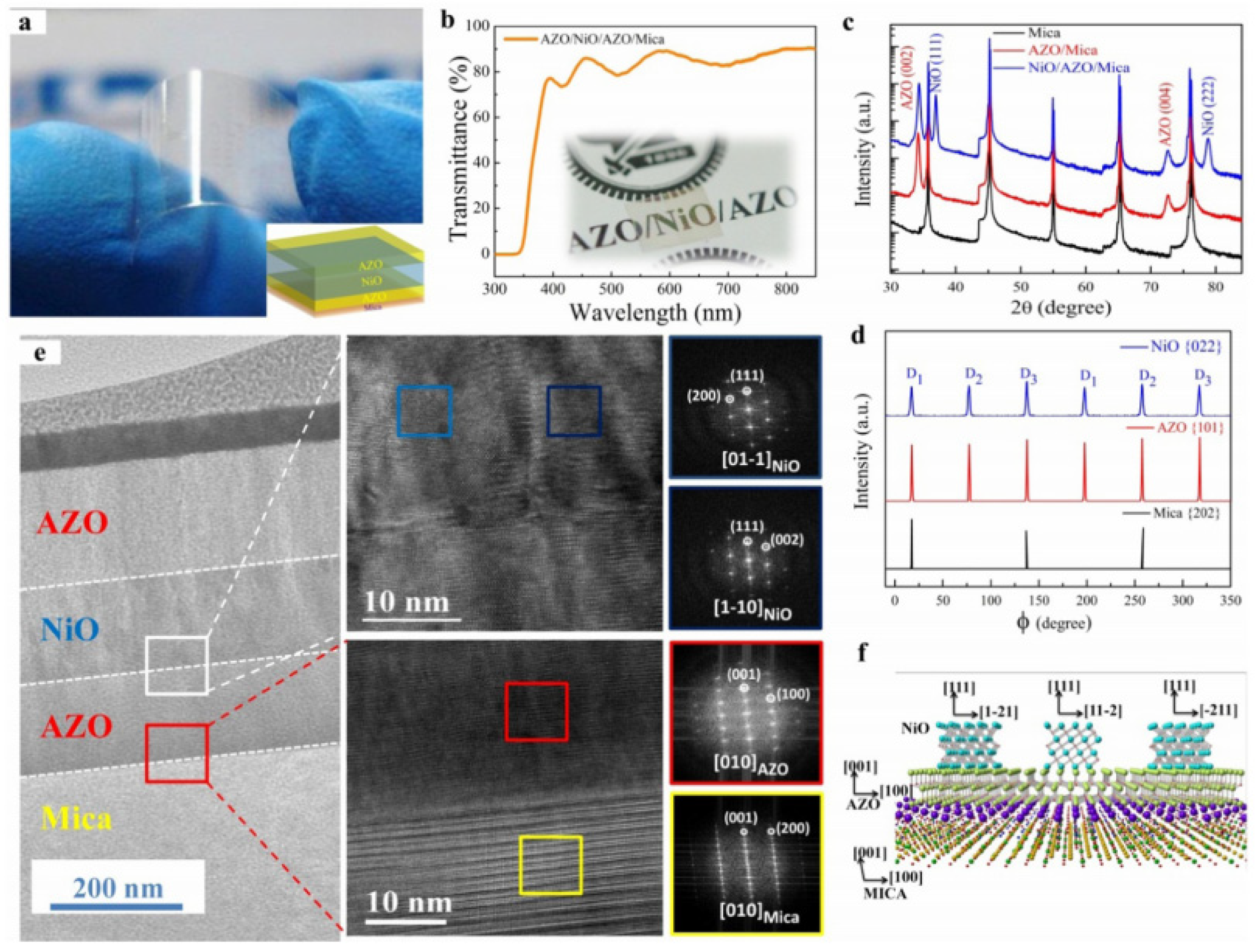
Figure 4.
Cu/pV3D3/Al/PES devices. Reprinted with permission from Ref. [48]. Copyright 2019 American Chemical Society. (a) Cu/pV3D3/Al/PES memristor. (b) Cross-sectional TEM image of the flexible pV3D3 memristor.
Figure 4.
Cu/pV3D3/Al/PES devices. Reprinted with permission from Ref. [48]. Copyright 2019 American Chemical Society. (a) Cu/pV3D3/Al/PES memristor. (b) Cross-sectional TEM image of the flexible pV3D3 memristor.

Figure 5.
The electrical and mechanical stabilities of the ITSs-based flexible memristor. Reprinted with permission from Ref. [54]. Copyright 2019 American Chemical Society. (a) A photograph of our flexible device under bending. (b) I–V characteristics under bending deformation with the radius of curvature rb = 5 mm. (c) Retention performance of the device under bending deformations with rb = 5 mm at Vread = 2 V. (d) Switching cycle tests at Vread = 2 V for the durability characteristics of the device.

Figure 6.
Ag/hBN/Cu foil flexible device [65]. (a) Ag/hBN/Cu foil/PET substrate device. (b) Cross-section TEM image, and the thickness of hBN is about ≈ 3 nm. (c) The electroforming process for hBN memory device with V forming ≈ 1.87 V. (d) The switching characteristics of the hBN memory device after electroforming process.
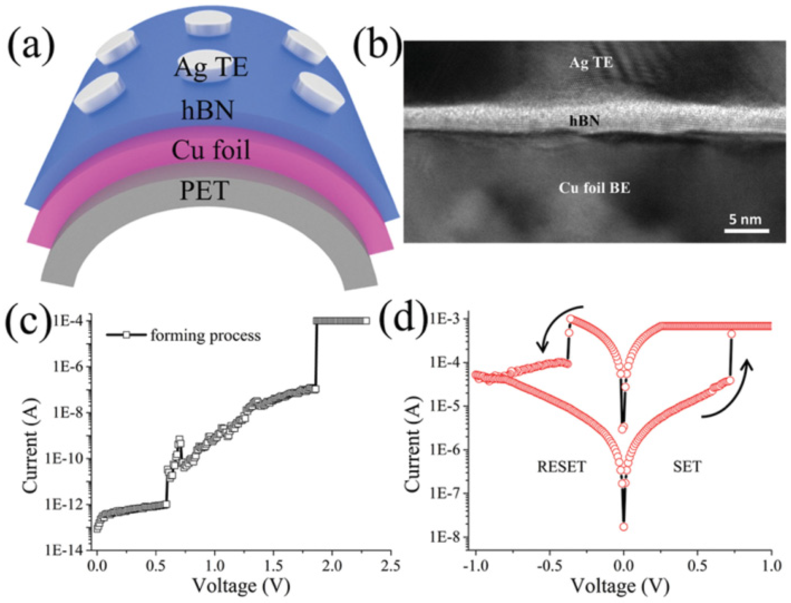
Figure 7.
Proposed fabrication process and schematic of a tungsten (W)/egg albumen/indium tin oxide (ITO)/polyethylene terephthalate (PET) memristor. Reprinted with permission from ref. [78]. Copyright 2019 American Chemical Society.
Figure 7.
Proposed fabrication process and schematic of a tungsten (W)/egg albumen/indium tin oxide (ITO)/polyethylene terephthalate (PET) memristor. Reprinted with permission from ref. [78]. Copyright 2019 American Chemical Society.

Figure 8.
Au/Mg/fibroin/Mg flexible device. Reprinted with permission from ref. [23]. Copyright 2016 John Wiley and Sons. (a) Optical images of the fibroin fibers and aqueous solution of fibroin. (b) Schematic of the transient resistive switching memory device. (c) Schematic diagram of the fabrication procedures for the fibroin substrates. (d) Schematic diagram of the fabrication procedures for the resistive switching devices.
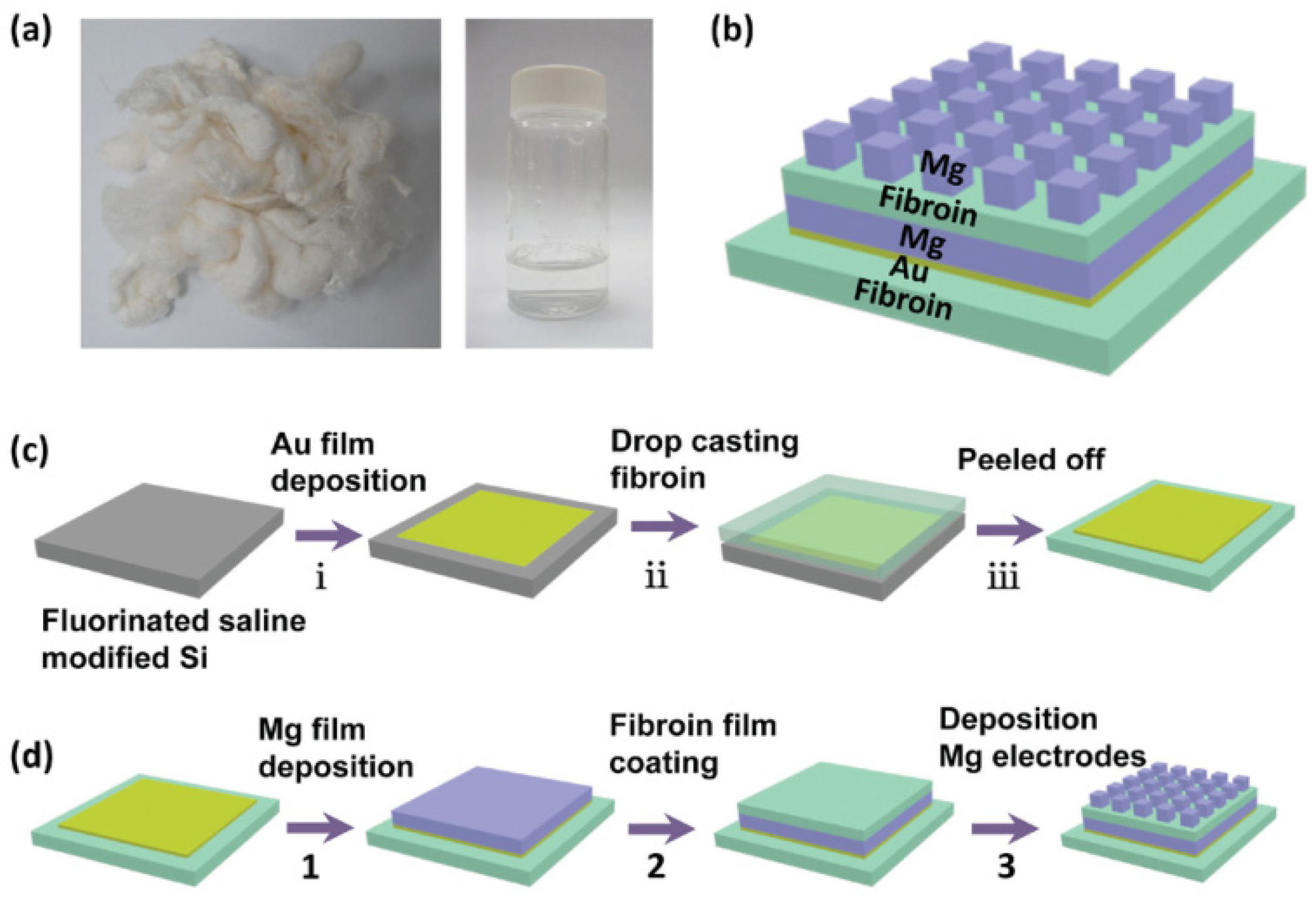
Figure 9.
Schematics of the fabrication process and the fabricated device. Reprinted with permission from ref. [82]. Copyright 2020 John Wiley and Sons. (a) Fabrication process of fibroin memristors on a Parylene-C film utilizing UV photolithography. (b) Close-in schematic of a single cell in the crossbar architecture.

Figure 10.
Au/Lignin/ITO/PET flexible device. Reprinted with permission from ref. [83]. Copyright 2017 American Chemical Society. (a) Schematic and structure of lignin in lignocellulose. (b) Schematic structure of flexible Au/Lignin/ITO/PET device. (c) Photograph of the memory array on flexible substrate.

Figure 11.
Pt/WOx/Ti flexible device. Reprinted with permission from ref. [93]. Copyright 2018 John Wiley and Sons. (a) Fabrication process using water-dissolution method. (b) Schematic diagrams of electrical measurement of Pt/WOx/Ti device transferred on PEN substrate. (c) The device is transferred on PEN substrate under bending. (d) Flexible printing paper, a glass dome hemisphere with a 3D surface, pectin substrate, and then onto skin and PDMS substrate.
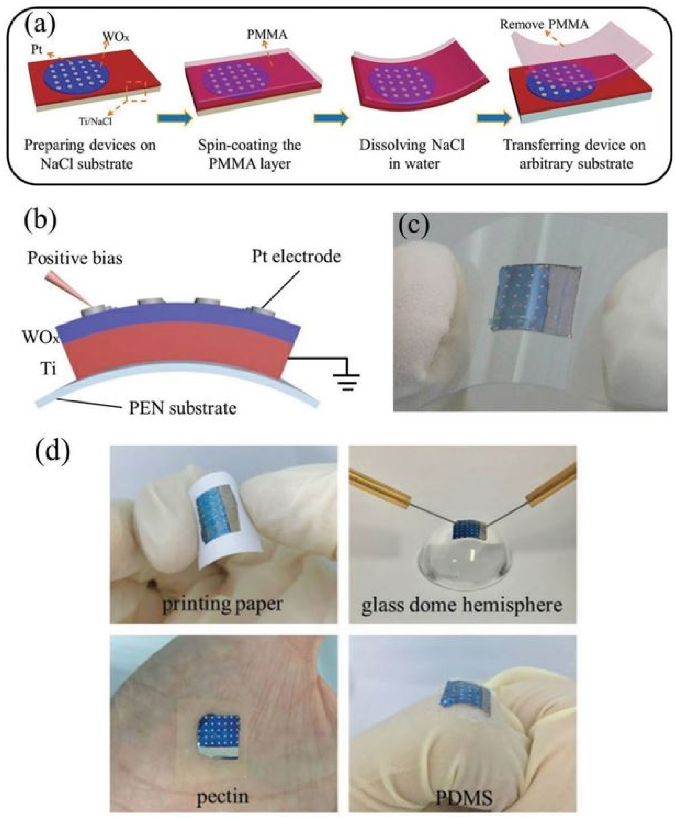
Figure 12.
3D stacked flexible memristor. Reprinted with permission from ref. [56]. Copyright 2020 John Wiley and Sons. (a) Schematic diagram of the proposed organic 3D Vmemristor based on parylene-C. (b) Polymer CVD process for fabricating parylene-C film. (c–j) Fabrication flow of the proposed organic 3D Vmemristor.
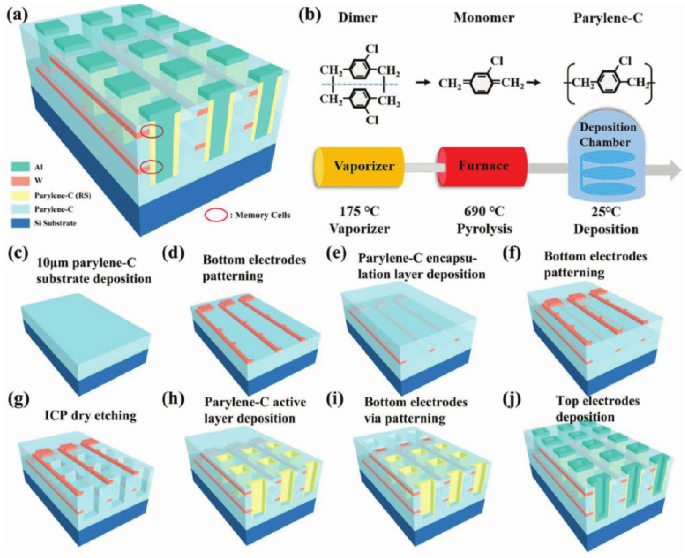
Figure 13.
Structures and working mechanism of biological synapses and electrical properties of the receptor-inspired counterpart [114]. (a) a-I Schematic diagram for the connection of two neurons by a synapse in the biological system and a-II, the working principle of the G-protein-linked receptor. (b) Schematic diagram. (c) Optical image of the flexible memristors. CS and rGO were used as the top and bottom layers of the device channels, respectively. (d–f) Characteristics for the devices with (d) rGO, (e) CS, and (f) rGO covered by CS as the channel materials.
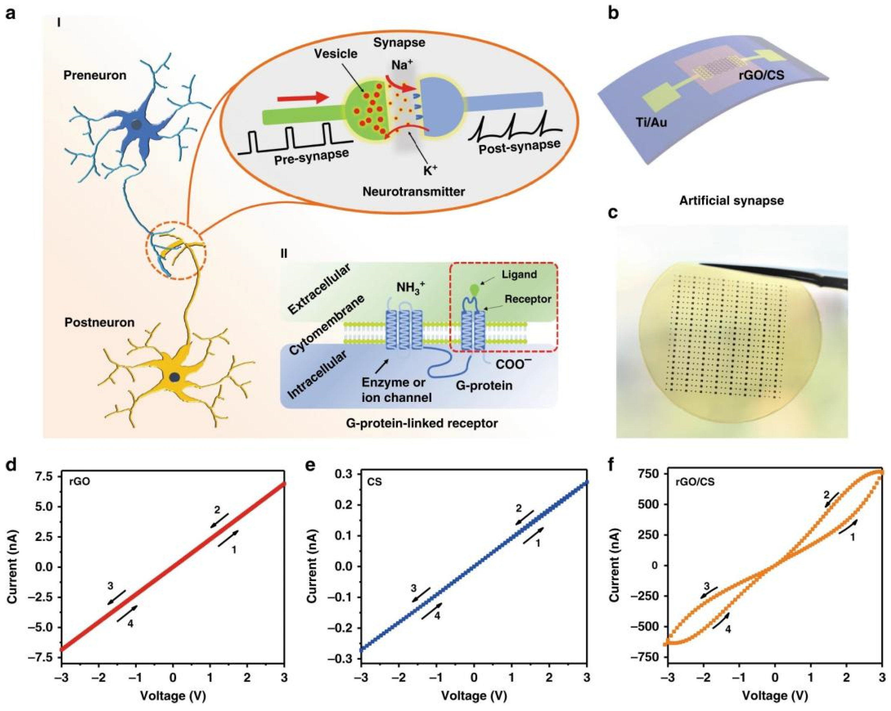
Figure 14.
Proposed model for working mechanism of the artificial synapse [114]. (a) Schematic diagram for the working mechanism of the memristor. The current is formed due to the hopping of protons provided by CS through functional groups and limited by the traps in rGO nanosheets. (b–d) Proposed model consisting of a number of face-to-face diodes for the memristor working in zero bias, forward bias, and reverse bias conditions, respectively.
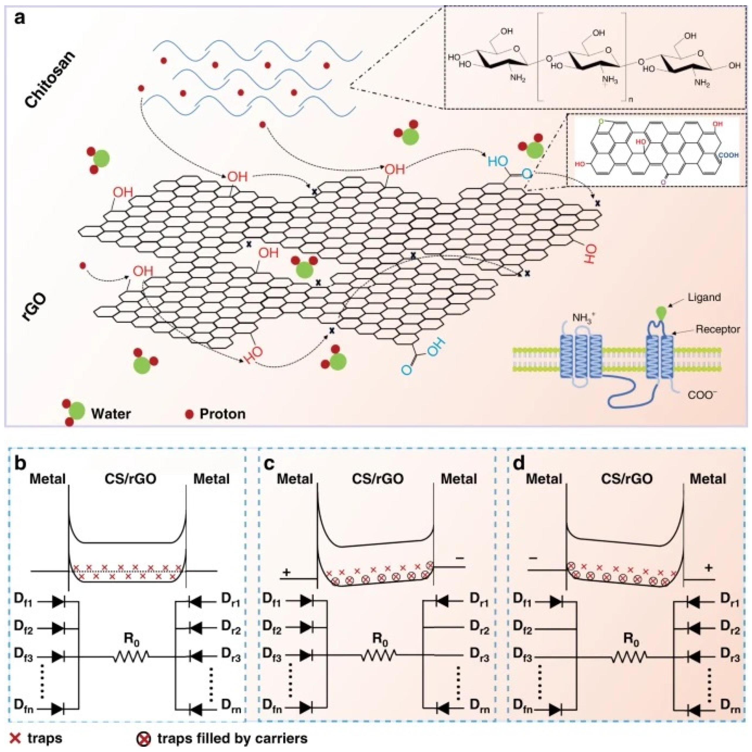
Figure 15.
Emulation of learning and forgetting process with the designed artificial synapse [114]. (a,b) The STP and LTP behaviors of the artificial synapse. (c,d) A demonstration of STM and LTM of the artificial synapses by putting letters “LH” and “X” into the matrix.
Figure 15.
Emulation of learning and forgetting process with the designed artificial synapse [114]. (a,b) The STP and LTP behaviors of the artificial synapse. (c,d) A demonstration of STM and LTM of the artificial synapses by putting letters “LH” and “X” into the matrix.
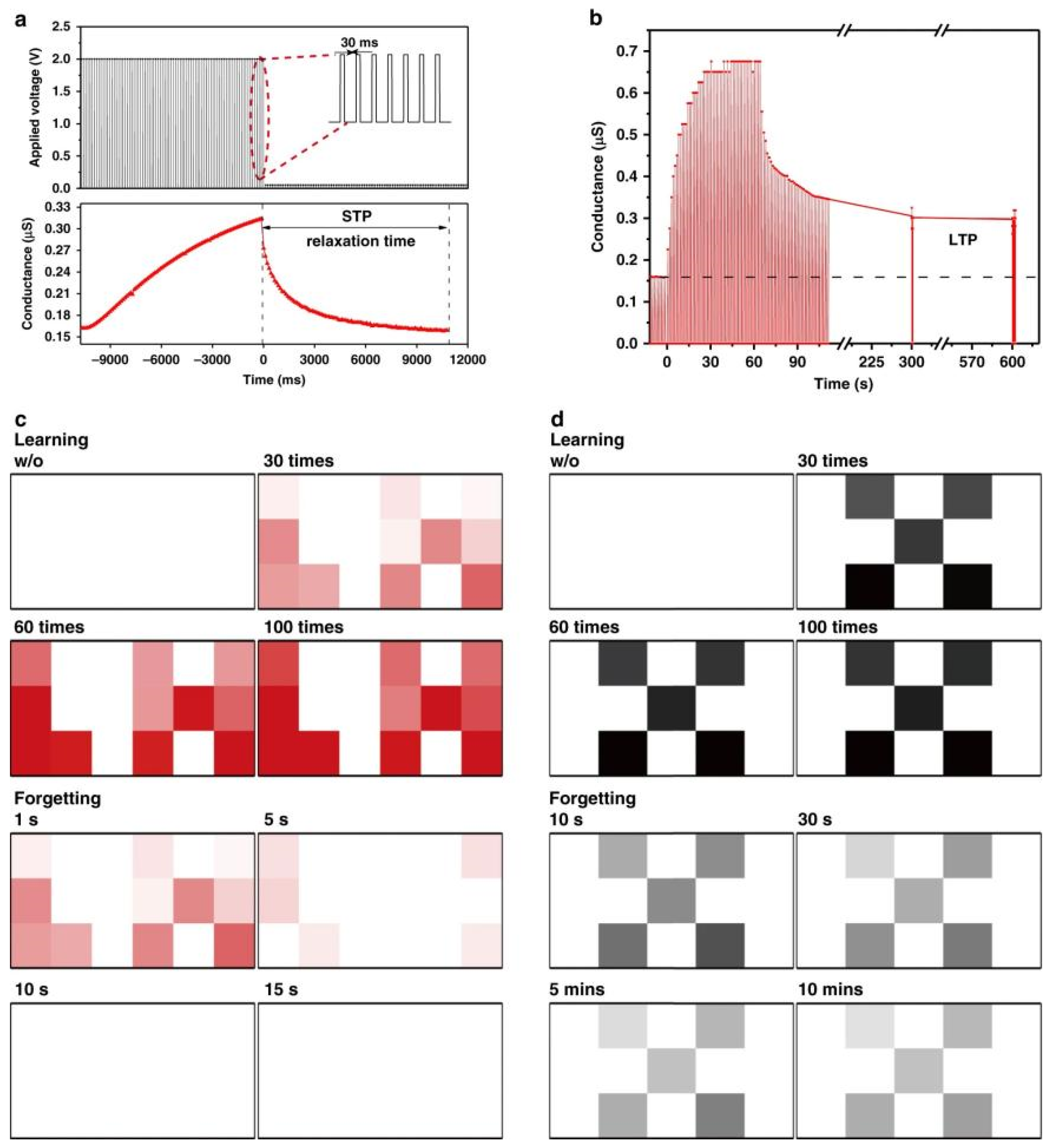

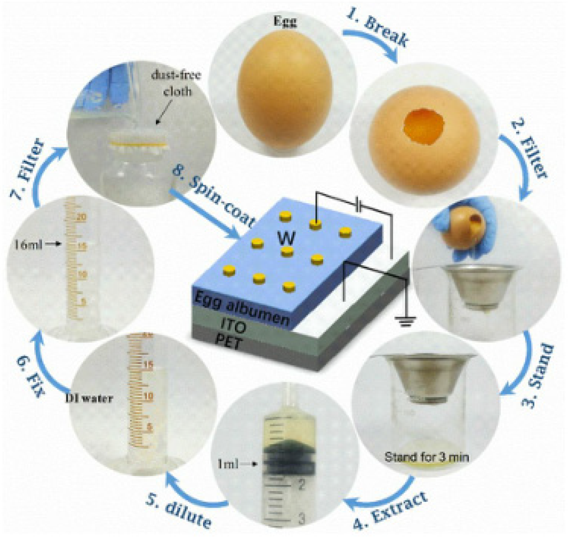
Table 1.
A summary of the flexible memristor materials.
| Materials | Advantages | Disadvantages | Reference | ||
|---|---|---|---|---|---|
| Flexible memristor material | Metals | Ti | Degradability | High cost | [27] |
| Pt | [23] | ||||
| Mg | [24] | ||||
| Ag | [25] | ||||
| W | [78] | ||||
| Oxides | ITO | Transparency | High cost | [29] | |
| ZnO | [31] | ||||
| AZO | [32] | ||||
| Flexible dielectric layer material | Metal oxide flexible memristor | TiO2 | High memristive performance | Poor flexibility | [37] |
| HfO2 | [38] | ||||
| ZnO | [44] | ||||
| Organic polymers flexible memristor | PEDOT:PSS | High flexibility | Unsustainable development | [47] | |
| PV3D3 | [48] | ||||
| PMMA | [53] | ||||
| PDDF-g-MWNTs | [55] | ||||
| Parylene-C | [56] | ||||
| Two-dimensional materials flexible memristor | Graphene | High flexibility | High cost | [62] [65] [69] [71] | |
| HBN | |||||
| MoS2 | |||||
| WS2 | |||||
| Biodegradable materials flexible memristor | BSA | High flexibility Low cost Sustainable development Biocompatibility | Poor tolerance Device performance needs to be improved | [24] | |
| Egg white protein | [78] | ||||
| Gelatin | [79] | ||||
| Fibroin | [23] | ||||
| Lignin | [82] | ||||
| DNA | [83] | ||||
| Flexible substrate material | Organic flexible substrate material | PET | Low cost | Poor heat resistance | [27] |
| PDMS | [24] | ||||
| PLGA | [89] | ||||
| A4 paper | [90] | ||||
| Inorganic flexible substrate material | Muscovite | High temperature resistance | Complex preparation process | [91] | |
| NaCl | [93] | ||||
Table 2.
A summary of the flexible memristors.
| Memristor | Retention Time (s) | SET/RESET Voltage (V) | ON/OFF Ratio | Stability | Flexibility | Reference |
|---|---|---|---|---|---|---|
| ITO/HfOx/ITO/PET | 105 | 0.4/−0.2 | ~40 | 108 pulse-mode switching cycles | Withstand a mechanical tensile stress of up to 2.12% | [30] |
| AZO/NiO/AZO/muscovite | 105 | 0.5 | >105 | Stable endurance to 103 cycles | Work at various bending radii down to 5 mm | [32] |
| ITO/TiO2/HfO2/Pt/PEN | 104 | 1.5/−1.5 | >10 | HRS and LRS resistances are estimated to be ≈ 3.2% and ≈ 3.0% | Withstand bending radius ranging from 70 to 10 mm | [43] |
| TiN/Al2O3/ZnO/Al2O3/TiN | >104 | 5 | >102 | Stable endurance > 104 cycles | Withstand a bending radius of up to 3 mm | [44] |
| 3D Al/parylene-C/W | >105 | 2.6/0.75 | >10 | Stable endurance > 300 cycles | Withstand bending conditions (radius <10 mm) | [56] |
| Ag/MgO-PVP-Gr/ITO | >104 | 4/−4 | 8.5 × 10³ | Stable endurance to 500 cycles | Withstand various bending cycles after 100, 250, 500 cycles | [48] |
| Ag TE/hBN/Cu/PET | 3 × 10³ | 0.72/−0.37 | 100 | Stable endurance to 550 cycles | Bending endurance ≈ 750 cycles | [65] |
| Ag/silk fibroin/Au/Parylene-C | 103 | 3/4 | 103–109 | Stable endurance to 30 cycles | Remains the same during bending over a cylinder with a radius of curvature of 1.3 mm | [82] |
Publisher’s Note: MDPI stays neutral with regard to jurisdictional claims in published maps and institutional affiliations. |
© 2021 by the authors. Licensee MDPI, Basel, Switzerland. This article is an open access article distributed under the terms and conditions of the Creative Commons Attribution (CC BY) license (https://creativecommons.org/licenses/by/4.0/).
Share and Cite
MDPI and ACS Style
Zhang, H.; Liu, R.; Zhao, H.; Sun, Z.; Liu, Z.; He, L.; Li, Y. Research Progress of Biomimetic Memristor Flexible Synapse. Coatings 2022, 12, 21. https://doi.org/10.3390/coatings12010021
AMA Style
Zhang H, Liu R, Zhao H, Sun Z, Liu Z, He L, Li Y. Research Progress of Biomimetic Memristor Flexible Synapse. Coatings. 2022; 12(1):21. https://doi.org/10.3390/coatings12010021
Chicago/Turabian StyleZhang, Huiling, Ruping Liu, Huiqing Zhao, Zhicheng Sun, Zilong Liu, Liang He, and Ye Li. 2022. "Research Progress of Biomimetic Memristor Flexible Synapse" Coatings 12, no. 1: 21. https://doi.org/10.3390/coatings12010021
Note that from the first issue of 2016, this journal uses article numbers instead of page numbers. See further details here.