
Effect of Conformal Coating on Electrochemical Migration Behavior of Multi-Layer Ceramic Capacitor for Automotives Based on Water Drop Test

1
Materials Research Centre for Energy and Clean Technology, Andong National University, 1375 Gyeongdong-ro, Andong 36729, Republic of Korea
2
School of Materials Science and Engineering, Andong National University, 1375 Gyeongdong-ro, Andong 36729, Republic of Korea
*
Author to whom correspondence should be addressed.
Coatings 2024, 14(3), 359; https://doi.org/10.3390/coatings14030359
Submission received: 14 February 2024
/
Revised: 12 March 2024
/
Accepted: 14 March 2024
/
Published: 18 March 2024
(This article belongs to the Special Issue Recent Advances in Surface Functionalisation)
Abstract
:A large amount of multi-layer ceramic capacitor (MLCC) is mounted inside a printed circuit board (PCB) constituting electronic components. The use of MLCC in electric vehicles and the latest mobile phones is rapidly increasing with the latest technology. Environments in which electronic components are used are becoming more diverse and conformal coatings are being applied to protect mounted components from these environments. In particular, MLCCs in electronic components mainly have voltage applied. They might be used in environments where humidity exists for various reasons. In a humid environment, electrochemical migration (ECM) will occur, with the cathode and anode on the surface of the MLCC encountering each other. This can result in product damage due to a short circuit. In this study, the effects of voltage, NaCl concentration, and distance between electrodes on a non-mount MLCC, surface mount MLCC, and solder pad pattern were evaluated using a water drop test (WDT). Based on the analysis of the effects of the presence of conformal coating, applied voltage, concentration of NaCl, and the distance between electrodes, a mechanism model for ECM behavior in MLCCs was proposed.
1. Introduction
Currently, the use of semiconductor devices is increasing in many industries [1]. Additionally, in the automotive industry, the proportion of electronic components has significantly increased due to the adoption of the latest technologies such as electric vehicles and autonomous driving. These electronic components range from those with simple functions to those requiring high reliability. Among them, the usage of MLCCs has rapidly increased. MLCCs are mainly used in power transmission devices, safety and convenience vehicle electronics, infotainment, and telematics systems. MLCCs are essential components in a variety of electronic devices, and their importance is rapidly increasing as more than 10,000 MLCCs are installed, especially within automotive applications. There is a growing demand for high reliability capable of withstanding harsh conditions such as high temperature, high pressure, and high humidity. The increasing prevalence of electric and hybrid vehicles is driving up the demand for high-voltage, high-capacity MLCCs. These high-voltage high-capacity MLCCs are applied in battery management systems (BMS), inverters, electric motor controls, etc. Furthermore, advancements in advanced driver assistance system (ADAS) technology, including autonomous driving, are significantly increasing the quantity and quality of MLCCs required in automobiles [2,3]. The main areas where MLCCs are applied in automotive electronic components are as follows: within the Engine Control Unit (ECU), they support various functions including timing control, fuel injection systems, ignition systems, and more; high-quality MLCCs are also used in complex infotainment systems, such as advanced audio systems and navigation; and high-performance MLCCs are essential for systems responsible for car safety such as ABS (anti-lock brake system), ESC (electronic stability control), and ADAS systems [3].
In the case of electronic components, reliability problems occur due to various environmental causes, such as temperature, humidity, atmospheric pressure, solar radiation, dust and sand, corrosive atmosphere, wind, rain, tsunami, vibration, shock, and ozone [4]. In particular, in the case of automobiles, characteristics of driving in a variety of environments, outdoor parking, and the existence of a consumer base in various regions are different from other products. As it is used in the external environment, it is difficult to specify one environment such as coastal areas, desert areas, industrial areas, and mountainous areas.
When the external environment of a PCB becomes corrosive, various problems can occur in the circuit and components when voltage is applied. Problems that can occur in PCBs include electromigration (EM), stress migration (SM), ECM, and conductive anode filament (CAF). Among them, in the case of ECM, when a corrosive environment containing electrolytes is formed under the condition that voltage is applied, a short circuit occurs due to the migration of dissolved metal ions from the anode and the formation of a metallic dendrite from the cathode to the anode [5,6,7,8]. This problem is divided into humid ECM and wet ECM depending on the form of electrolyte. In the case of a humid ECM, a thin layer of electrolytes that are not visible is adsorbed on the surface. In the case of wet ECM, a visible layer of condensed electrolytes occurs, which can be induced by water droplets due to various causes [9,10,11].
The behavior of the ECM is affected by the composition and concentration of the electrolyte. Common electrolytes that can infiltrate PCBs from external sources include halogenated compounds and sulfates. In the case of Cl− ions, the dissolution rate at the anode increases with increasing concentration. However, the probability of dendrite formation decreases beyond a certain concentration. This is because dissolved tin ions do not form dendrites. Instead, they form tin hydroxide precipitates that can obstruct ion movement. As the concentration increases further beyond the point of precipitate formation, re-dissolution of precipitates and dendritic growth of Sn at the cathode can occur, leading to a short circuit [12,13]. Meanwhile, for ECM in sulfate environments, similar to results reported for Cl− ions, no dendritic growth occurs at a certain concentration. Only a precipitate is formed. However, when the concentration is increased beyond a certain point, dendritic growth occurs again with increasing risk of a short circuit [14,15,16,17,18].
The ECM on the PCB is mainly short-circuited by the formation of Sn dendrites, which are more resistant when they are alloyed with metals such as Cu or Ag than pure Sn [16]. Therefore, for solder to bond to the PCB, various alloys of Sn are being used to increase the resistance of the ECM [19,20,21,22,23,24,25,26].
On the other hand, the outer layer of MLCCs consists of metal layers stacked in the order of copper, nickel, and tin, with the outermost layer being a Sn-plated layer that is mounted onto the PCB [27]. The appearance of the surface layer after this mounting process increases the risk to the ECM as the pure Sn layer is exposed to the external environment.
The surface layer of the electrode part of the MLCC is composed of a Sn layer and is bonded to the PCB through various processes, such as hand soldering, reflow soldering, and wave soldering using various fluxes such as a Rosin-based flux, water-soluble flux, and no-clean flux. In products like electric vehicles, multiple PCBs are interconnected, each mounting various components and undergoing different processes. This makes it difficult to control the environment of the PCB surface [28,29].
Methods for evaluating ECM generated from MLCC include THBT (Temperature Humidity Bias Test) and WDT (Water Drop Test). In THBT, tests using time and voltage as variables were conducted under the acceleration conditions of 85% Rh and 85 °C. However, this evaluation method has the disadvantage of requiring a long time and making it difficult to change environmental conditions [30,31]. On the other hand, since WDT can be measured through various solution concentrations and applied voltages, it is possible to determine behavior depending on environmental conditions. Contrary to the general trend, ECM occurrence is not necessarily more common with higher voltages and electrolyte concentrations. In experiments where NaCl concentrations were set to 10 ppm, 100 ppm, and 1000 ppm, and 3 V and 12 V were applied, it was observed that at a concentration of 10 ppm, more migration due to ECM occurred at 3 V compared to 12 V. However, at 100 ppm, the migration due to ECM was greater at 12 V than at 3 V. At a higher concentration of 1000 ppm, the trend of migration due to ECM decreased for both 3 V and 12 V compared to the previous concentrations [12]. As such, a problem was raised that it is difficult to clearly define the environment in which ECM occurs. In addition, warnings have been raised that ECM may emerge as a serious problem in the electronics industry in the future due to the diversity of manufacturing environments, miniaturization of electronic devices, and increased sensitivity to contamination [32].
In ISO 26262 [33], semiconductors are graded from A to D based on ASIL (Automotive Safety Integration Level) for the necessary functional verification and safety verification of automotive semiconductors, with the highest stability being grade D [34]. Additionally, the IPC (Institute for Printed Circuits) categorizes semiconductor components into Classes, distinguishing grades for each component, with reliability classified from Class 1 to Class 3, where Class 3 indicates a high reliability [33]. Conformal coating is typically manufactured using high polymer resins. It is applied to components that require high reliability. These conformal coatings are made of various materials such as Urethane, Silicone, Epoxy, Acrylic, Parylene, and so on [35].
As described above, MLCCs become harsher as the number of devices required increases. They are used in various environments as technology advances toward electric vehicles and autonomous vehicles. Automotive electronic components are exposed to unpredictable variables from the soldering process to actual usage environments and require high reliability to ensure safety. To meet these requirements, conformal coatings are applied, but how they resist and react to ECMs have been poorly studied.
Therefore, in this study, we measured and analyzed the ECM behavior of surface mount MLCCs and non-mount MLCCs and solder pad patterns using the WDT test in a NaCl solution to simulate the corrosive environment caused by the spraying of snow removal agents on roads driven by automobiles and incoming salt by the sea. This work aims to propose the ECM mechanism in surface mount MLCCs and non-mount MLCCs by component analysis.
2. Experimental Methods
2.1. Specimen
Specimens used in this study were surface-mounted MLCC and non-mount MLCC of PCB products for automobile navigation and manufactured solder pad patterns. For surface mount MLCC specimens, the PCB was cut to an appropriate size for testing. Tests were conducted for corresponding MLCCs, a device with spacing between Sn electrodes of 400 μm, 800 μm, and 1200 μm. In the case of non-mount MLCC, a device with a spacing of 800 μm between Sn electrodes was used. In the case of the solder pad pattern, it was a pad-type test piece made of Sn–37%Pb solder. Pad spacing was 300 μm and 1300 μm.
2.2. Water Drop Test
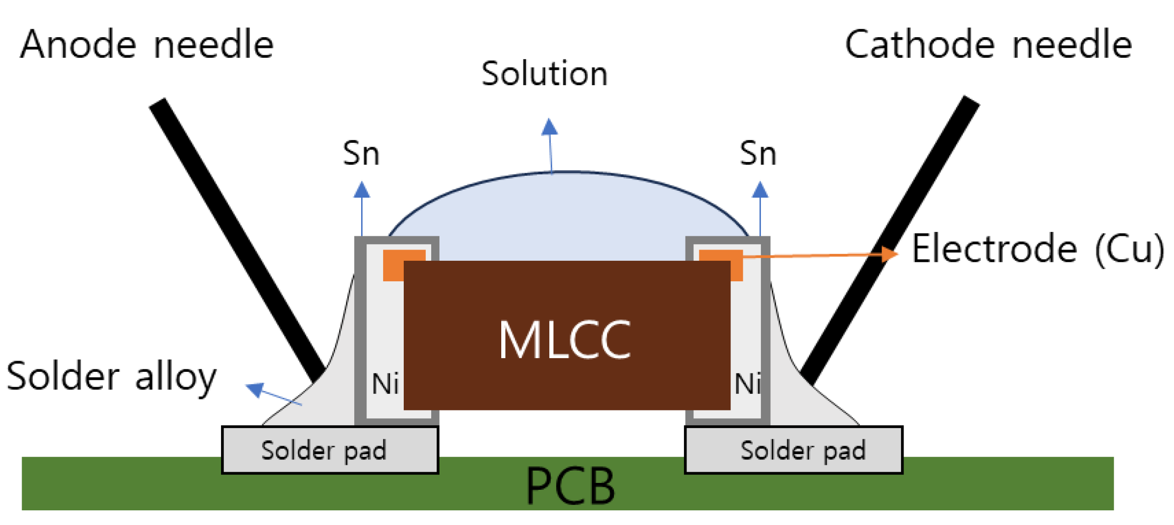
Figure 1 shows a schematic diagram of WDT for a surface mount MLCC specimen (for non-mount MLCCs, anode and cathode needles were connected to Sn electrodes; for solder pad pattern, they were connected to the ends of pads). Approximately 1 μL of test solution was dropped on the top of both electrodes. Anode and cathode needles were then connected to a WDT device (Model 2401, Keithley Instruments, Solon, OH, USA) and voltage was applied to obtain a current–time graph. Test solutions were 0.1% NaCl and 0.3% NaCl. The applied voltage ranged from 1.5 V to 12 V. All tests were conducted at room temperature.
2.3. Surface Appearance Analysis
A stereo microscope (SV-35, Sometech, Seoul, Republic of Korea) was used to observe dendrite formation during the WDT test. To analyze dendrites generated after the WDT test, specimens were observed using FE-SEM (MIRA3 XMH, Tescan, Brno, Czech Republic). The shape and composition of the product were analyzed using EDS (VEGA II LMU, Tescan, Brno, Czech Republic). After WDT, all analyses were performed without cleaning.
2.4. FT-IR Analysis
To determine the type of conformal coating of surface-mounted MLCC on PCB products for automobile navigation, FTIR (FT/IR-4200, JASCO, Tokyo, Japan) was used for analysis. The scan rate was 2 mm/s and the data interval was 1 cm−1. Measurement was performed with a wave number ranging from 650 cm−1 to 4000 cm−1.
3. Results
3.1. ECM Behavior of Surface Mount MLCC by Water Drop Test
Figure 2 shows current–time graphs measured by applying voltages of 3 V, 5 V, and 12 V, respectively, to surface mount MLCCs with a Sn electrode spacing of 800 μm in a 0.1% NaCl solution. While an initial current peak occurred immediately upon applying a voltage, the current decreased over time as the test duration increased. Increasing the applied voltage resulted in a similar decrease in the current, although the initial current peak increased. It should be noted that the test time was limited to less than 200 s to allow the test solution to dry before evaporation. No failure was observed under any voltage conditions.
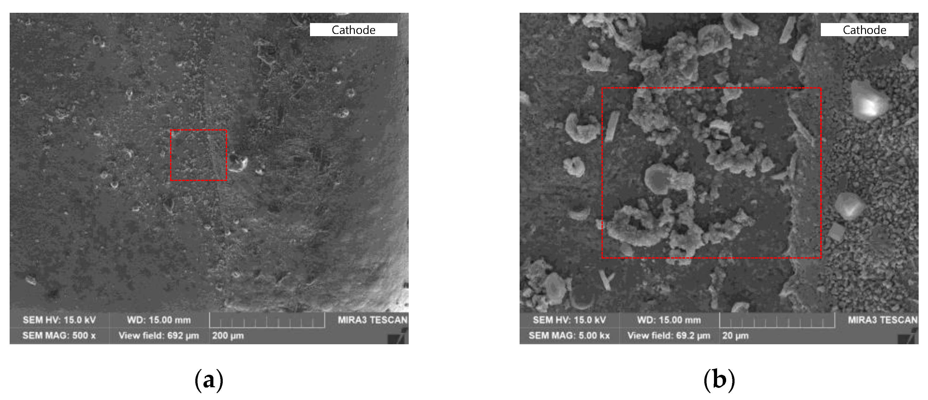
Figure 3 shows the surface appearance of dendrites formed on surface mount MLCC by water drop test under the same conditions as shown in Figure 2. Regarding test conditions, 5 V was applied to surface mount MLCC specimens with an electrode distance of 800 μm in a 0.1% NaCl solution. The appearance of the specimen was observed using SEM after the test. Figure 3a is an image observed at ×500 magnification of the area around the cathode after the WDT. No dendrite structure was observed. However, many spherical particles were observed. Figure 3b is an image of the same area observed at ×5000 magnification. It could be seen that many particles were attached to each other. However, they did not come into contact with the cathode.
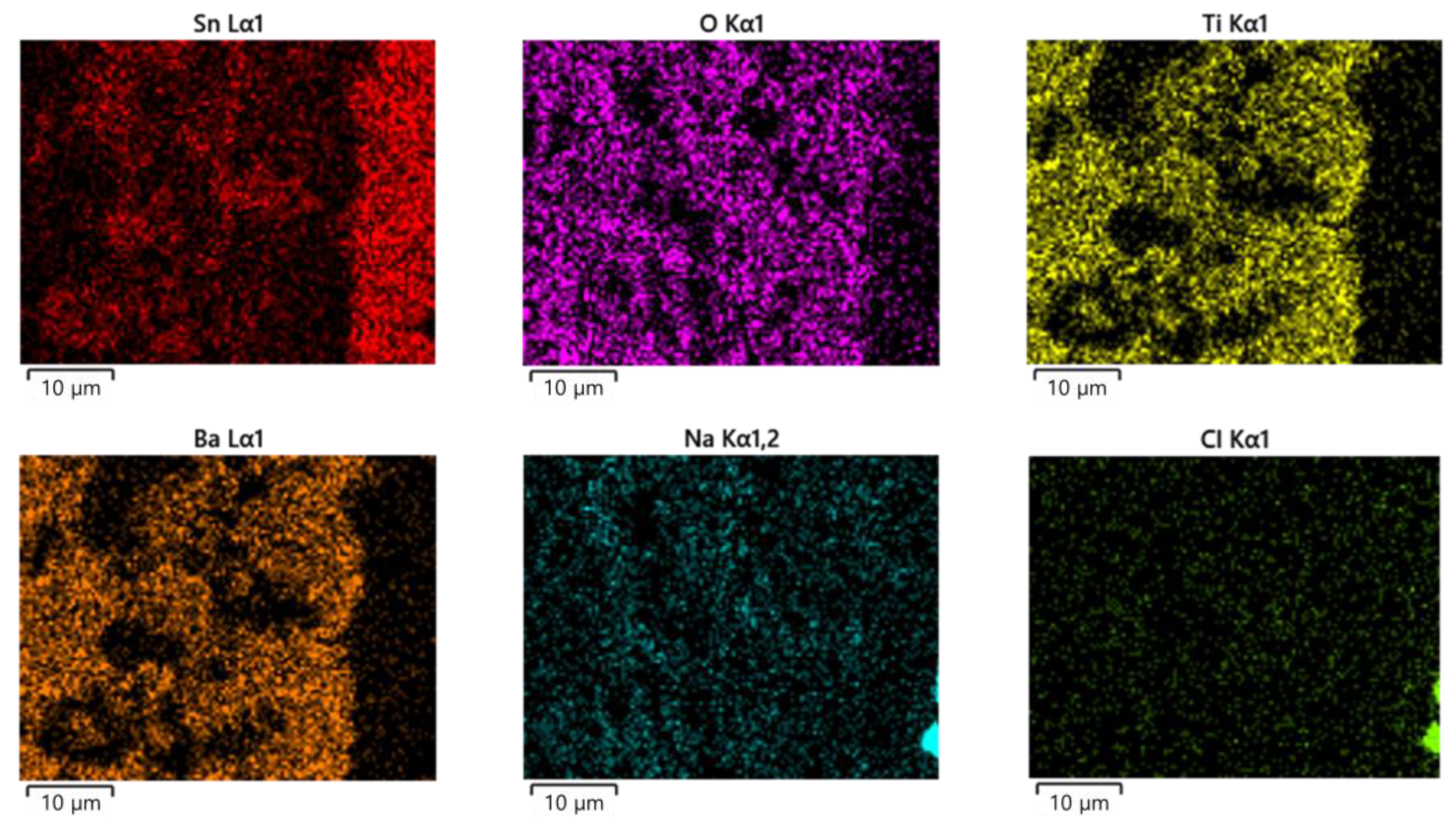
Figure 4 shows results of EDS analysis for the area shown in Figure 3b. In Figure 4, the red color shows the Sn component distribution. The vertical red part on the right was the Sn coating layer of the cathode electrode of the MLCC specimen. The particle part of the spherical shape shown in Figure 3b also had a high Sn component, which was confirmed to be the Sn component migrated by dissolution from the anode. The purple color in Figure 4 shows the oxygen component distribution. The oxygen concentration was low in the cathode electrode of the MLCC specimen on the right, while a high oxygen concentration was detected in the ceramic part of the MLCC. This distribution should be interpreted in conjunction with Ba and Ti. What is important to note here is that Ba and Ti appear to be depleted. This trend is consistent with the area where a large amount of Sn was detected, as shown in the Sn component analysis results. In other words, the Sn component that dissolved from the anode moved to the cathode and aggregated in a spherical shape. When viewed overlapping with the distribution of the oxygen component, it appeared that Sn and O components overlapped. This meant that the Sn that had migrated from the anode did not exist in a metallic state, but rather reacted with H2O in the solution and existed as tin oxide. Therefore, a large amount of tin had migrated towards the cathode. However, it did not form a metallic dendrite. It was isolated as tin oxide, which was supported by morphology observations shown in Figure 3b.
Figure 5 shows the effect of applied voltage on a current–time graph for a surface mount MLCC (electrode distance: 800 μm) by water drop test in 0.3% NaCl. As shown in the figure, when the concentration of NaCl solution was increased to 0.3%, a current peak occurred due to the application of voltage. However, the current decreased rapidly with time. This result showed a similar trend to the previous Figure 2, suggesting that the ECM phenomenon due to dendrite growth did not occur.
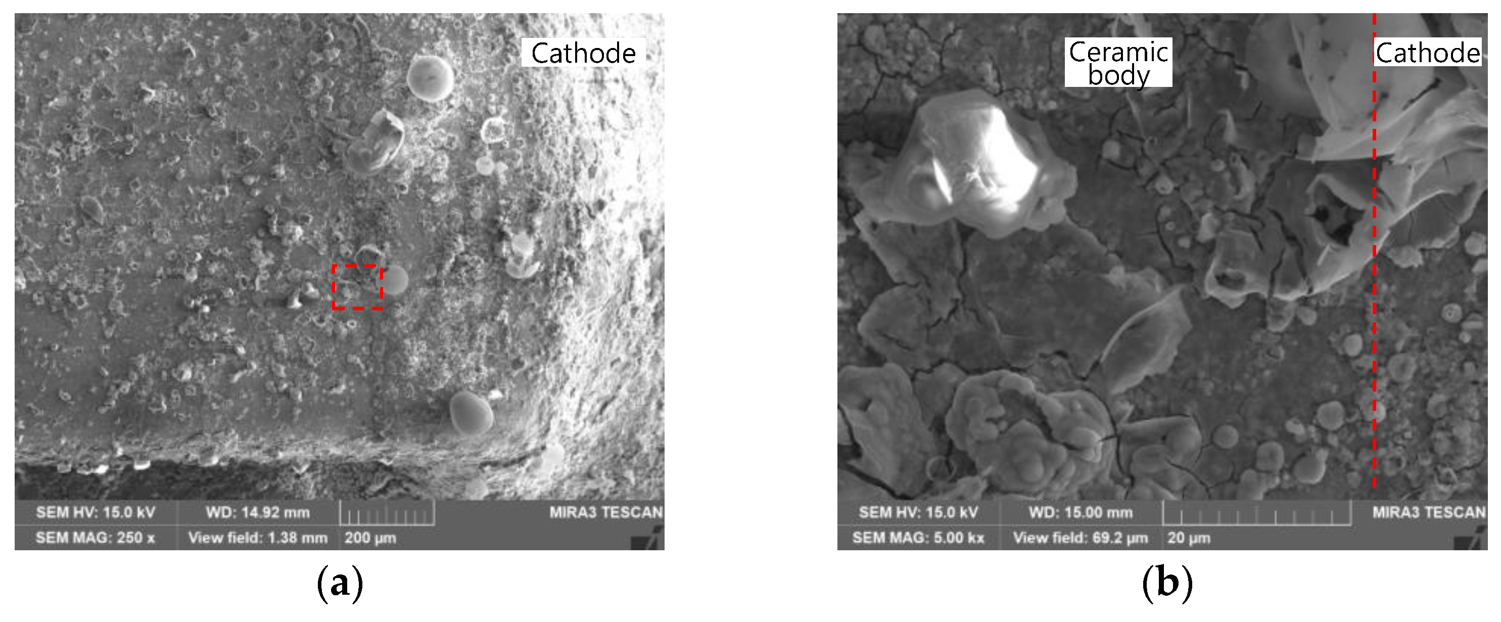
Figure 6 is an SEM image of the surface after WDT for a specimen used for the current–time test in Figure 5 with an applied voltage of 5 V. In Figure 6a, a low magnification image, spherical particles are observed near the cathode side on the right. In the enlarged image (Figure 6b) of this area (red box in Figure 6a), a large number of agglomerated particles and cracks were observed at the electrode and MLCC ceramic areas. In other words, when the NaCl concentration of the solution increased, the amount of adhesion products also increased around the cathode. However, no dendrites were observed at the cathode. These products were not formed up to the anode. They mainly existed around the cathode.
Figure 7 shows the elemental distribution of a surface mount MLCC (electrode distance: 800 μm) by water drop test in 0.3% NaCl at 5 V. The reason why Ba and Ti, as main components of the MLCC ceramic area, were not detected on the entire surface might be because a material composed of Sn and O covered the entire surface. The fact that the distribution of oxygen overlapped more with the distribution of Sn than with Ba or Ti indicated that Sn oxide was formed, in which Sn was combined with oxygen. Results similar to those obtained from the WDT in 0.1% NaCl shown in Figure 4 were also observed under conditions of high NaCl concentration. Metallic dendrites were not formed.
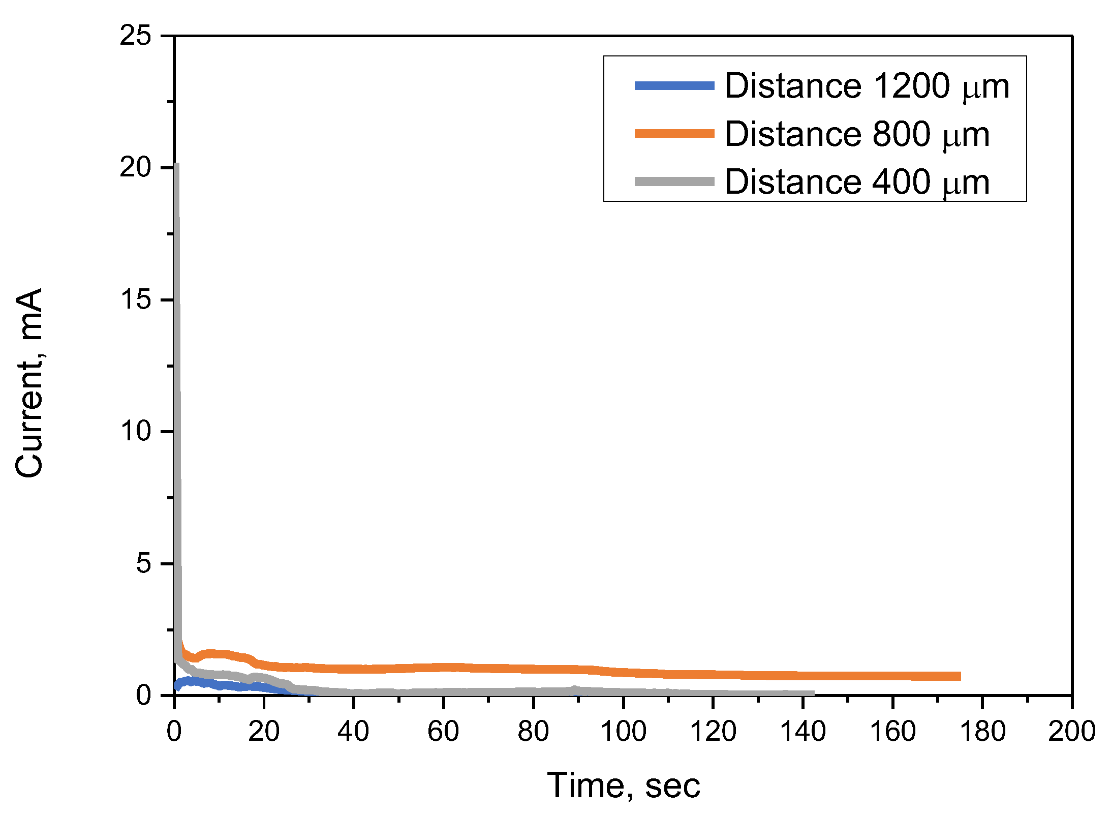
Figure 8 shows the effect of electrode distance on the current–time graph for a surface mount MLCC by water drop test in 0.3% NaCl at 3 V. Even when the spacing between electrodes was increased to 1200 μm, no increase in current was observed by WDT. When WDT was performed by reducing the spacing between electrodes to 400 μm, no increase in current was observed. In other words, the ECM phenomenon was not observed in WDT for surface mount MLCC.
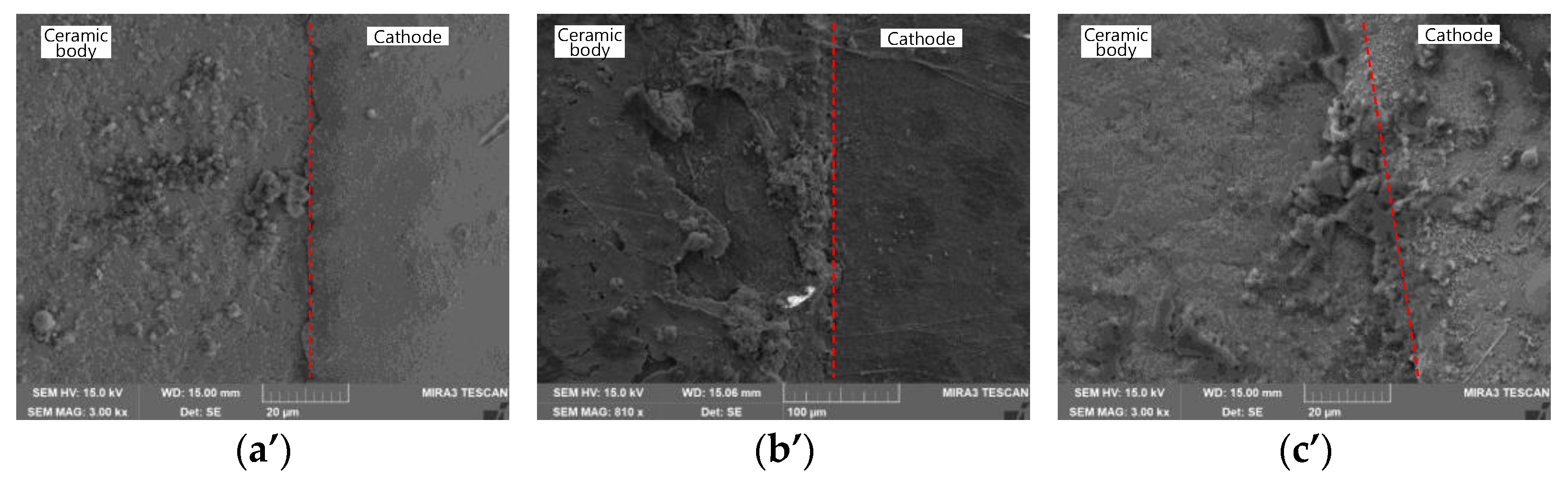
Figure 9 shows the surface appearance of a surface mount MLCC after a water drop test using 0.3% NaCl at 3 V. Figure 9a,a’ are photos for the electrode distance at 400 μm. The anode section on the left was heavily damaged in appearance and the MLCC ceramic section in the middle was found to have damaged material adhering to it (Figure 9a). When observing the cathode part enlarged (Figure 9a’), many small spherical particles were formed near the cathode. Furthermore, when the appearance was examined after WDT of an MLCC with an electrode spacing distance of 800 μm like the above, the material in the anode part was damaged. It moved to the cathode and adhered to the top of the MLCC ceramic with the material on the ceramic area cracked (Figure 9b). When observing the anode part in detail (Figure 9b’), a surface layer was detached. In the case of 1200 μm for electrode spacing distance (Figure 9c,c’), the anode area was damaged and migrated particles were attached near the electrode.
Figure 10 shows the elemental distribution of a surface mount MLCC for Figure 9b after a water drop test using 0.3% NaCl at 5 V. Typically, Ba, Ti, and O as main components of the MLCC’s ceramic part appeared to match well. The Sn component that migrated from the anode was mainly distributed at the left side of the cracked layer. Comparing distribution patterns of Sn and O, their high degree of correlation suggested formation of Sn-O compounds, consistent with previously described results. Na and Cl components were distributed on the whole surface because the specimen was not cleaned after WDT.
3.2. ECM Behavior of Non-Mount MLCC by Water Drop Test
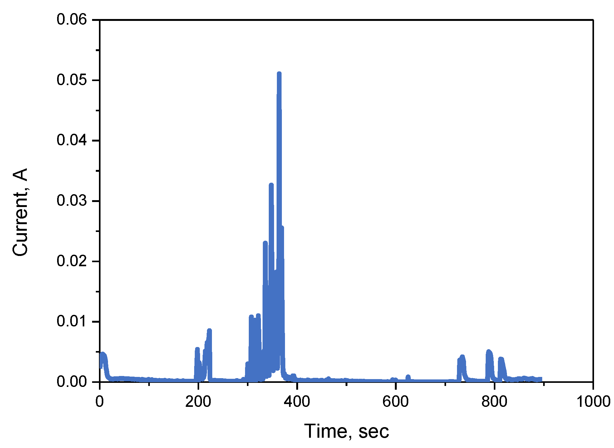
Figure 11 shows current–time and resistance–time graphs of non-mount MLCC (electrode distance: 800 μm) by WDT in 0.3% NaCl solution at an applied voltage of 1.5 V. A rapid rise in current and a decrease in resistance were observed at 215 s after starting the test.
Figure 12 shows the surface appearance of dendrites formed for non-mount MLCC with an electrode spacing of 800 μm by WDT in 0.3% NaCl at an applied 1.5 V. As shown in Figure 12a, the anode region was damaged due to the dissolution of metallic ions. It could be confirmed that dissolved ions were formed as products on the upper surface of the MLCC ceramic. These products were also observed to be connected to the cathode, as shown in Figure 12b. Upon further magnification, as shown in Figure 12c, the formation of typical metallic dendrites was confirmed (The red dashed line represents the interface between the ceramic body and the cathode). As these dendrites grew from the cathode to the anode and became electrically connected, the ECM phenomenon, as depicted in Figure 11, occurred, where the current increased rapidly and the resistance decreased sharply.
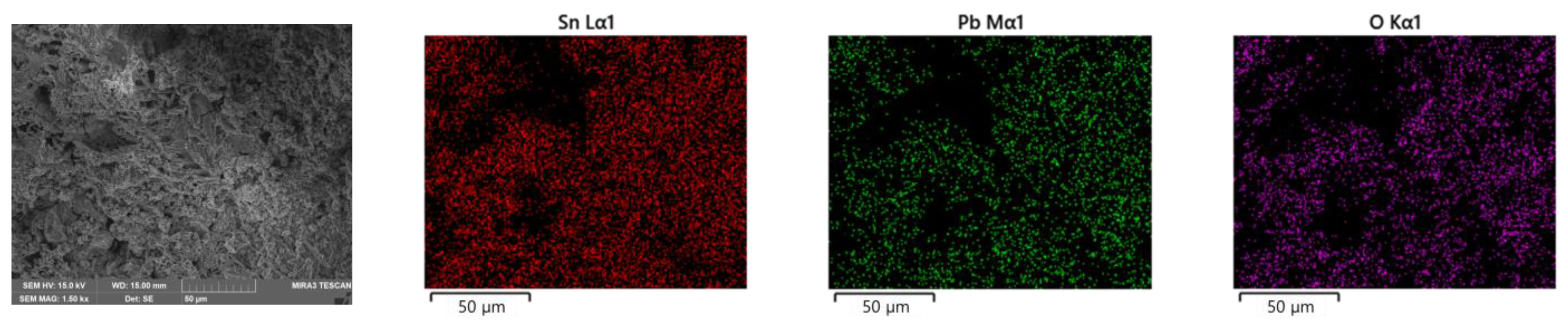
Figure 13 shows the distribution of each component measured by EDS for the region in Figure 12c. For Sn, it confirms that the Sn component is widely distributed in addition to the dendrite shape. Importantly, the distribution of oxygen, Ba, and Ti components appeared depleted in the region where dendrites were formed, confirming that metallic Sn dendrites were formed rather than Sn oxides (the Sn-depleted area on the right side of Figure 13 looked like a vertical band due to electrode step difference).
4. Discussion
To summarize the above results, a WDT using salt water for surface mount MLCCs on a PCB for automotive navigation did not produce dendrites due to ECM regardless of the concentration of the test solution, the distance between the cathode and anode, or the applied voltage. However, for non-mount MLCCs, ECM occurred even under a typical condition of WDT and the current increased rapidly as metallic dendrites grew and connected from the cathode to the anode. Therefore, it is necessary to examine the effects of applied voltage, solution concentration, and distance between electrodes on the occurrence of ECM.
To determine the effects of various conditions on ECM formation, WDT was performed. Figure 14 shows the effects of applied voltage on the ECM of solder pad patterns with an electrode distance of 300 μm by WDT in 0.3% NaCl at room temperature. Figure 14a shows a current–time graph according to the applied voltage. It could be seen that the time for the current to rise rapidly decreased as the applied voltage increased. The time when the current reached 0.1 A was measured and defined as the failure time. The relationship with the failure time according to the applied voltage is shown in Figure 14b. It was found that the failure time decreased linearly as the applied voltage increased. The linear relationship is y = −8.76x + 408.41, and the coefficient of determination (R2) showed a value of 0.8542. In this way, the ECM for the solder pad was by WDT. Under the same conditions, failure occurred quickly when a high voltage was applied. At a certain low voltage, the time of occurrence was delayed. However, failure occurred eventually.
Figure 15 shows the effect of applied voltage on the surface appearance of dendrites formed by water drop test in 0.3% NaCl for solder pad patterns (electrode distance: 300 μm) from Figure 14. When the applied voltage was low (Figure 15a), the dendrite formed had a typical dendritic form. However, an increase in voltage changed the dendritic form from a typical dendrite to a lumped form. In the case of an applied voltage of 12 V (Figure 15d), the dendrite covered up the ceramic area of MLCC between two electrodes. This behavior was due to accelerated dissolution of Sn at the anode and formation of metallic dendrite from the cathode following the below equations in the case of Sn:
At the anode, Sn → Sn2+ + 2e
At the cathode, Sn2+ + 2e → Sn
Figure 16 shows the elemental distribution of a solder pad pattern with an electrode distance of 300 μm by WDT in 0.3% NaCl. For Sn and Pb, it could be seen that the main contribution to dendrite formation was Sn, which was the main component of the solder. In addition, the distribution of the oxygen component showed that the main component of the dendrite was not a Sn-O compound, but a metallic composition (Si was a component of the pad specimen substrate). Therefore, it could be seen that the product formed by an increase in the applied voltage not only caused an electrical short circuit, but also caused a short circuit due to the easy growth of the metallic dendrite even when the applied voltage was relatively low.
Figure 17 shows a current–time graph obtained by applying 5 V in 0.3% NaCl solution to a solder pad manufactured with a spacing of 1300 μm between electrodes. When the electrode distance was increased, the failure time occurred at 363.7 s. Therefore, the cause of failure in surface mount MLCC was not related to the distance between the anode and cathode. Figure 18 shows the surface appearance and elemental distribution of dendrites formed by water drop test in 0.3% NaCl at 5 V for electrode distance of 1300 μm of solder pad pattern. A large amount of dendrites were formed, which were confirmed to be metallic dendrites by surface analysis.
Meanwhile, according to many research results on ECM [36], ECM is easily generated when corrosive substances are in solution. However, ECM is generated even when the relative humidity is controlled using distilled water as a corrosive environment [36]. Therefore, the cause of ECM not occurring in surface mount MLCCs cannot be considered to be related to the concentration of the corrosion solution.
For this reason, it should be noted that surface mount MLCCs mounted on automotive navigation PCBs were manufactured with a different process than conventional non-mount MLCCs. In other words, after mounting various electronic devices such as MLCCs on the PCB board, a conformal coating was applied to metallic joints, wires, or soldering areas. Materials used for this coating include urethane, silicone, epoxy, acrylic, and para-xylylene [35]. Therefore, FTIR analysis was performed on the surface of the surface mount MLCC used in this study. As shown in Figure 19, a silicone-like spectrum was detected on the MLCC surface. A silicone-based conformal coating provides excellent performance in high temperature and humid environments. It also has electrical insulation properties, so it is used in the automotive industry where high voltages are required. The maintenance of integrity by such silicone-based conformal coatings prevents ECM. However, it is important to note that in externally operated vehicles, the conformal coating may degrade under various conditions, and there is a possibility that ECM may occur.
Figure 20 shows the surface appearance of a surface mount MLCC (a) before the test and (b) after the water drop test in 0.3% NaCl at 5 V. Before the water drop test (Figure 20a), the ceramic area between the electrodes of a surface mount MLCC showed a uniformly conformal coated surface with silicone type. However, after the water drop test (Figure 20b), an irregular surface at the anode was observed and a conformal coating failed due to a strong voltage applied in the electrolyte. The coating then peeled off and cracked as shown in Figure 9b. However, the conformal coating at the cathode side was still stable.
Based on the results and discussion, we could propose the mechanism of dendrite growth and protection by conformal coating in MLCCs as shown in Figure 21. Figure 21a presents the mechanism of ECM behavior observed in non-mount MLCCs. As shown in Equations (1) and (2), at the anode, the Sn present on the surface of the electrode dissolves into Sn ions and migrates to the cathode, where it receives electrons from the cathode to become metallic Sn and grow dendrite. As a result, when dendrite growth reaches the anode, electrical short circuits occur, leading to material failure. As shown in Figure 21b, in the case of a surface mount MLCC, the mechanism for ECM behavior occurring in conformal-coated MLCC is shown as follows.
Step 1: When voltage is applied in a corrosive environment, a part of the conformal coating present on the anode is damaged by the applied voltage.
Step 2: As shown in Equation (1), Sn is ionized and dissolved in an aqueous solution by the applied voltage. It then migrates toward the cathode.
Step 3: Since the integrity of the conformal coating on the cathode side is maintained with an electrical insulation, a reduction reaction as shown in Equation (2) does not occur and metallic dendrite is not formed. On the other hand, tin oxide is formed through a reaction with water present in an aqueous solution as shown in Equation (3):
Sn2+ + H2O → SnO + 2H+
Figure 21c shows a side view of a surface mount MLCC. When the electrolyte was formed on the surface of the MLCC during WDT and voltage was applied to the anode and cathode, voltage-induced coating failure occurred first, exposing the anode. The Sn present on the anode surface was then dissolved into Sn ions, which were directed toward the cathode. However, these tin ions did not form metallic Sn, but precipitated on the coating layer in the form of Sn oxide and failed to form a short circuit. Thus, ECM occurrence became difficult.
5. Conclusions
As a result of analyzing the effects of applied voltage, distance between electrodes, solution concentration, and conformal coating by performing a water drop test using salt water for a surface mount MLCC on automobile navigation PCB, non-mount MLCC, and solder pad pattern, the following conclusions were obtained.
- In the case of a MLCC without conformal coating, regardless of the water drop test conditions, the Sn from the anode dissolved and migrated to the cathode, forming a metallic dendrite, resulting in the ECM phenomenon.
- In the case of a surface mount MLCC with conformal coating, ECM phenomenon by the water drop test did not occur due to the following mechanisms: ① When a voltage was applied, a part of the conformal coating on the anode was damaged by the applied voltage. ② Sn was ionized and dissolved in an aqueous solution by the applied voltage. It then migrated toward the cathode. ③ The integrity of the conformal coating on the cathode side was maintained with electrical insulation without metallic dendrite formation. However, it reacted with water present in the aqueous solution to form tin oxide. Thus, ECM occurrence became difficult.
The metallic dendrite growing from the cathode to the anode can cause electrical shorts, thereby degrading the reliability of electronic components and shortening their lifespan. In the case of automobiles, the failure of electrical components due to ECM is safety-related and can be life-threatening, so reliability issues must be minimized. We have continued to conduct research on the deterioration of conformal coating and a Temperature Humidity Bias Test (THBT).
Author Contributions
Conceptualization, S.W. and Y.-R.Y.; methodology, S.W.; validation, S.W. and Y.-R.Y.; formal analysis, Y.-S.K.; investigation, S.W.; resources, Y.-R.Y.; data curation, S.W. and Y.-R.Y.; writing—original draft preparation, S.W. and Y.-R.Y.; writing—review and editing, Y.-S.K.; visualization, S.W.; supervision, Y.-S.K.; project administration, Y.-R.Y. and Y.-S.K.; funding acquisition, Y.-S.K. All authors have read and agreed to the published version of the manuscript.
Funding
This research was supported by a grant from the 2023–2024 research funds of Andong National University, and the Korea Institute for Advancement of Technology (KIAT) grant funded by the Korea Government (MOTIE) (P0008458, HRD Program for Industrial Innovation).
Institutional Review Board Statement
Not applicable.
Informed Consent Statement
Not applicable.
Data Availability Statement
Data are contained within the article.
Acknowledgments
The authors would like to thank HYUNDAI MOBIS and HL Mando for supplying the materials.
Conflicts of Interest
The authors declare no conflicts of interest.
References
- Marati, N.; Gupta, R.G.; Vaithilingam, B. Multilayer ceramic capacitors crisis management in automotive industry. In Proceedings of the 2020 IEEE International Conference on Power Electronics Smart Grid and Renewable Energy (PESGRE2020), Cochin, India, 2–4 January 2020. [Google Scholar] [CrossRef]
- Hong, K.; Lee, T.H.; Suh, J.M.; Yoon, S.-H.; Jang, H.W. Perspective and challenges in multilayer ceramic capacitors for next generation electronics. J. Mater. Chem. C 2019, 32, 1–21. [Google Scholar] [CrossRef]
- Xu, X.; Gurav, A.S.; Lessner, P.M.; Randall, C.A. Robust BME Class-I MLCCs for Harsh-Environment Applications. IEEE Trans. Ind. Electron. 2011, 58, 2636–2643. [Google Scholar] [CrossRef]
- IEC 60068-1; Environmental Testing—Part 1: General and Guidance. International Electrotechnical Commission: Geneve, Switzerland, 2023.
- Tan, C.M.; Chen, H.H.; Wu, J.P.; Sangwan, V.; Tsai, K.Y.; Huang, W.C. Root cause analysis of a printed circuit board (PCB) failure in a public transport communication system. Appl. Sci. 2022, 12, 640. [Google Scholar] [CrossRef]
- Kohman, G.T.; Hermance, H.W.; Downes, G.H. Silver migration in electrical insulation. Bell Syst. Tech. J. 1955, 34, 1115–1147. [Google Scholar] [CrossRef]
- Noh, B.I.; Jung, S.B. Behaviour of electrochemical migration with solder alloys on printed circuit boards (PCBs). Circuit World 2008, 34, 8–13. [Google Scholar] [CrossRef]
- Jung, J.Y.; Lee, S.B.; Joo, Y.C.; Lee, H.Y.; Park, Y.B. Anodic dissolution characteristics and electrochemical migration lifetimes of Sn solder in NaCl and Na2SO4 solutions. Microelectron. Eng. 2008, 85, 1597–1602. [Google Scholar] [CrossRef]
- IPC-TM-650; Assessment of Susceptibility to Metallic Dendritic Growth: Uncoated Printed Wiring. Institute for Interconnecting and Packaging Electronic Circuits: Bannockburn, IL, USA, 2015.
- IPC-TM-650; Solder Mask—Resistance to Electrochemical Migration. Institute for Interconnecting and Packaging Electronic Circuits: Bannockburn, IL, USA, 2015.
- Krumbein, S.J. Metallic electromigration phenomena. IEEE Trans. Compon. Hybrids Manuf. Technol. 1988, 11, 5–15. [Google Scholar] [CrossRef]
- Minzari, D.; Jellesn, M.S.; Moller, P.; Ambat, R. On the electrochemical migration mechanism of tin in electronics. Corros. Sci. 2011, 53, 3366–3379. [Google Scholar] [CrossRef]
- Zhong, X.; Zhang, G.; Qiu, Y.; Chen, Z.; Zou, W.; Guo, X. In situ study the dependence of electrochemical migration of tin on chloride. Electrochem. Commun. 2013, 27, 63–68. [Google Scholar] [CrossRef]
- Yoo, Y.R.; Nam, H.S.; Jung, J.Y.; Lee, S.B.; Park, Y.B.; Joo, Y.C.; Kim, Y.S. Effect of Ag and Cu additions on the electrochemical migration susceptibility of Pb-free solder in Na2SO4 solution. Corros. Sci. Technol. 2007, 2, 50–55. [Google Scholar]
- Medgyes, B.; Szabo, P.; Tamasi, P.; Gal, L.; Harsanyi, G. Electrochemical migration of Cu and Sn in Na2SO4 environment. In Proceedings of the 2016 39th International Spring Seminar on Electronics Technology (ISSE), Pilsen, Czech Republic, 18–22 May 2016. [Google Scholar] [CrossRef]
- Vianco, P.T. Corrosion issues in solder joint design and service. Weld. J. 1999, 78, 39–46. [Google Scholar]
- Medgyes, B.; Kiss, R.; Szurdan, S.; Rigler, D.; Gal, L.; Berenyi, R.; Harsanyi, G. Electrochemical migration investigations on Sn-Sb solder alloys using 3.5wt% NaCl solution. In Proceedings of the 2017 40th International Spring Seminar on Electronics Technology (ISSE), Sofia, Bulgaria, 10–14 May 2017. [Google Scholar] [CrossRef]
- Yu, D.Q.; Jillek, W.; Schmitt, E. Electrochemical migration of Sn-Pb and lead free solder alloys under distilled water. J. Mater. Sci. Mater. Electron. 2006, 17, 219–227. [Google Scholar] [CrossRef]
- Ready, W.J.; Turbini, L.J.; Nickel, R.; Fischer, J. A novel test circuit for automatically detecting electrochemical migration and conductive anodic filament formation. J. Electron. Mater. 1999, 28, 1158–1163. [Google Scholar] [CrossRef]
- Yoo, Y.R.; Kim, Y.S. Difference of potential range formed at the anode between water drop test and temperature humidity bias test to evaluate electrochemical migration of solders for printed circuit board. Corros. Sci. Technol. 2023, 22, 153–163. [Google Scholar] [CrossRef]
- Huang, M.; Zhang, Z.; Zhao, N.; Yang, F. Migration behavior of indium atoms in Cu/Sn-52In/Cu interconnects during electromigration. J. Mater. Res. 2015, 30, 3316–3323. [Google Scholar] [CrossRef]
- Kang, H.; Rajendran, S.H.; Jung, J.P. Low melting temperature Sn-Bi solder: Effect of alloying and nanoparticle addition on the microstructural, thermal, interfacial bonding, and mechanical characteristics. Metals 2021, 11, 364. [Google Scholar] [CrossRef]
- Medgyes, B.; Roman, E.; Bohnert, A.; Szurdan, S.; Zhong, X.; Harsanyi, G. Electrochemical migration investigations on SAC-Bi-xMn solder alloys. In Proceedings of the 2018 IEEE 24th International Symposium for Design and Technology in Electronic Packaging (SIITME), Iasi, Romania, 25–28 October 2018. [Google Scholar] [CrossRef]
- Liao, B.; Jia, W.; Sun, R.; Chen, Z.; Guo, X. Electrochemical migration behavior of Sn-3.0Ag-0.5Cu solder alloy under thin electrolyte layers. Surf. Rev. Lett. 2019, 26, 1850208. [Google Scholar] [CrossRef]
- Jung, J.Y.; Lee, S.B.; Joo, Y.C.; Lee, H.Y.; Park, Y.B. Effect of ionization characteristics on electrochemical migration lifetimes of Sn-3.0Ag-0.5Cu solder in NaCl and Na2SO4 solutions. J. Electron. Mater. 2008, 37, 1111–1118. [Google Scholar] [CrossRef]
- Li, S.; Wang, X.; Liu, Z.; Jiu, Y.; Zhang, S.; Geng, J.; Chen, X.; Wu, S.; He, P.; Long, W. Corrosion behavior of Sn-based lead-free solder alloys: A review. J. Mater. Sci. Mater. Electron. 2020, 31, 9076–9090. [Google Scholar] [CrossRef]
- Pan, M.J.; Randall, C.A. A brief introduction to ceramic capacitors. IEEE Electr. Insul. Mag. 2010, 26, 44–50. [Google Scholar] [CrossRef]
- Verdingovas, V.; Jellsen, M.S.; Ambat, R. Influence of sodium chloride and weak organic acids (flux residues) on electrochemical migration of tin on surface mount chip components. Corros. Eng. Sci. Technol. 2010, 48, 426–435. [Google Scholar] [CrossRef]
- Laadjal, K.; Cardoso, A.J.M. Multilayer ceramic capacitors: An overview of failure mechanisms, perspectives, and challenges. Electronics 2023, 12, 1297. [Google Scholar] [CrossRef]
- Francisc, S. Study of ceramic capacitor technology link to electro chemical migration in automotive electronics. In Proceedings of the 2020 IEEE 26th International Symposium for Design and Technology in Electronic Packaging (SIITME), Pitesti, Romania, 21–24 December 2020. [Google Scholar] [CrossRef]
- Gu, J.; Azarian, M.H.; Pecht, M.G. Failure prognostics of multilayer ceramic capacitors in temperature-humidity-bias condition. In Proceedings of the 2008 International Conference on Prognostics and Health Management, Denver, CO, USA, 6–9 October 2008. [Google Scholar] [CrossRef]
- Takemoto, T.; Latanision, R.M.; Eagar, T.W.; Matsunawa, A. Electrochemical migration tests of solder alloys in pure water. Corros. Sci. 1997, 39, 1415–1430. [Google Scholar] [CrossRef]
- ISO 26262-2; Part 2: Management of Functional Safety. International Organization for Standardization: Geneve, Switzerland, 2018.
- IPC-6011; Generic Performance Specification for Printed Bards. International Organization for Standardization: Bannockburn, IL, USA, 1966.
- Byram, J. Conformal Coating, Printed Circuits Handbook, 6th ed.; Coombs, C.F., Ed.; McGraw Hill: New York, NY, USA, 2008; Volume 1, pp. 41.1–41.17. [Google Scholar]
- Vesely, P.; Klimtova, M.; Fros, D. Electrochemical migration issues related to improper solder mask application. In Proceedings of the 2022 45th International Spring Seminar on Electronics Technology (ISSE), Vienna, Austria, 11–15 May 2022. [Google Scholar] [CrossRef]
Figure 1.
Schematic diagram of water drop test for surface mount MLCC.

Figure 2.
Effect of applied voltage on current–time graph for surface mount MLCC (Sn electrode distance: 800 μm) by water drop test (test solution: 0.1% NaCl).
Figure 2.
Effect of applied voltage on current–time graph for surface mount MLCC (Sn electrode distance: 800 μm) by water drop test (test solution: 0.1% NaCl).

Figure 3.
Surface appearance of the dendrites formed for surface mount MLCC (electrode distance: 800 μm) by water drop test (applied voltage of 5 V in 0.1% NaCl): (a) ×500 (the red box is zoom-in area in (b)) and (b) ×5000 (surface analysis on the red box was shown in Figure 4).
Figure 3.
Surface appearance of the dendrites formed for surface mount MLCC (electrode distance: 800 μm) by water drop test (applied voltage of 5 V in 0.1% NaCl): (a) ×500 (the red box is zoom-in area in (b)) and (b) ×5000 (surface analysis on the red box was shown in Figure 4).

Figure 4.
Elemental distribution on the red box area of Figure 3b of surface mount MLCC (electrode distance: 800 μm) by water drop test in 0.1% NaCl at 5 V.
Figure 4.
Elemental distribution on the red box area of Figure 3b of surface mount MLCC (electrode distance: 800 μm) by water drop test in 0.1% NaCl at 5 V.

Figure 5.
Effect of applied voltage on current–time graph for surface mount MLCC (electrode distance: 800 μm) by water drop test in 0.3% NaCl.
Figure 5.
Effect of applied voltage on current–time graph for surface mount MLCC (electrode distance: 800 μm) by water drop test in 0.3% NaCl.

Figure 6.
Surface appearance of dendrites formed on surface mount MLCC (electrode distance: 800 μm) by water drop test in 0.3% NaCl at 5 V: (a) ×500 (the red box is zoom-in area in (b)) and (b) ×5000 (red dotted line is the boundary between the cathode and the ceramic body).
Figure 6.
Surface appearance of dendrites formed on surface mount MLCC (electrode distance: 800 μm) by water drop test in 0.3% NaCl at 5 V: (a) ×500 (the red box is zoom-in area in (b)) and (b) ×5000 (red dotted line is the boundary between the cathode and the ceramic body).

Figure 7.
Elemental distribution of surface mount MLCC (electrode distance: 800 μm) by water drop test in 0.3% NaCl at 5 V.
Figure 7.
Elemental distribution of surface mount MLCC (electrode distance: 800 μm) by water drop test in 0.3% NaCl at 5 V.

Figure 8.
Effect of electrode distance on current–time graph for surface mount MLCC by water drop test in 0.3% NaCl at 3 V.
Figure 8.
Effect of electrode distance on current–time graph for surface mount MLCC by water drop test in 0.3% NaCl at 3 V.

Figure 9.
The surface appearance of surface mount MLCC after water drop test using 0.3% NaCl at 3 V (red dotted line is the boundary between the cathode and the ceramic body): (a,a’) electrode distance: 400 μm, (b,b’) electrode distance: 800 μm, and (c,c’) electrode distance: 1200 μm.
Figure 9.
The surface appearance of surface mount MLCC after water drop test using 0.3% NaCl at 3 V (red dotted line is the boundary between the cathode and the ceramic body): (a,a’) electrode distance: 400 μm, (b,b’) electrode distance: 800 μm, and (c,c’) electrode distance: 1200 μm.


Figure 10.
Elemental distribution of surface mount MLCC for Figure 9b after water drop test using 0.3% NaCl at 5 V (electrode distance: 800 μm).
Figure 10.
Elemental distribution of surface mount MLCC for Figure 9b after water drop test using 0.3% NaCl at 5 V (electrode distance: 800 μm).

Figure 11.
(a) Current–time graph and (b) resistance–time graph of non-mount MLCC (electrode distance: 800 μm) by water drop test in 0.3% NaCl at 1.5 V.
Figure 11.
(a) Current–time graph and (b) resistance–time graph of non-mount MLCC (electrode distance: 800 μm) by water drop test in 0.3% NaCl at 1.5 V.

Figure 12.
Surface appearance of the dendrites formed for non-mount MLCC (electrode distance: 800 μm) by water drop test in 0.3% NaCl at 1.5 V: (a) ×176 (the red box is zoom-in area in (b)), (b) ×500 (the red box is zoom-in area in (c)), and (c) ×5000 (red dotted line is the boundary between the cathode and the ceramic body).

Figure 13.
Elemental distribution of non-mount MLCC (electrode distance: 800 μm) by water drop test in 0.3% NaCl at 1.5 V.
Figure 13.
Elemental distribution of non-mount MLCC (electrode distance: 800 μm) by water drop test in 0.3% NaCl at 1.5 V.

Figure 14.
Effect of applied voltage on the ECM of solder pad patterns (electrode distance: 300 μm) by water drop test in 0.3% NaCl at room temperature: (a) current–time curve and (b) applied voltage vs. time to failure (the red dotted line is a trend line).
Figure 14.
Effect of applied voltage on the ECM of solder pad patterns (electrode distance: 300 μm) by water drop test in 0.3% NaCl at room temperature: (a) current–time curve and (b) applied voltage vs. time to failure (the red dotted line is a trend line).

Figure 15.
Effect of applied voltage on surface appearance of the dendrites formed by water drop test in 0.3% NaCl for solder pad patterns (electrode distance: 300 μm and the red dotted line is the boundary between the cathode and the ceramic body); (a) 3 V, (b) 5 V, (c) 7 V, and (d) 12 V.
Figure 15.
Effect of applied voltage on surface appearance of the dendrites formed by water drop test in 0.3% NaCl for solder pad patterns (electrode distance: 300 μm and the red dotted line is the boundary between the cathode and the ceramic body); (a) 3 V, (b) 5 V, (c) 7 V, and (d) 12 V.

Figure 16.
Elemental distribution of solder pad pattern (electrode distance: 300 μm) by water drop test in 0.3% NaCl.
Figure 16.
Elemental distribution of solder pad pattern (electrode distance: 300 μm) by water drop test in 0.3% NaCl.

Figure 17.
Current–time graph of solder pad pattern (electrode distance: 1300 μm) by water drop test in 0.3% NaCl at 5 V.
Figure 17.
Current–time graph of solder pad pattern (electrode distance: 1300 μm) by water drop test in 0.3% NaCl at 5 V.

Figure 18.
Surface appearance and elemental distribution of dendrites formed by water drop test in 0.3% NaCl at 5 V for electrode distance of 1300 μm of solder pad pattern.
Figure 18.
Surface appearance and elemental distribution of dendrites formed by water drop test in 0.3% NaCl at 5 V for electrode distance of 1300 μm of solder pad pattern.

Figure 19.
FTIR spectrum of surface mount MLCC.

Figure 20.
Surface appearance of surface mount MLCC (a) before the test and (b) after water drop test in 0.3% NaCl at 5 V.
Figure 20.
Surface appearance of surface mount MLCC (a) before the test and (b) after water drop test in 0.3% NaCl at 5 V.

Figure 21.
Proposed model of (a) dendrite growth of non-mount MLCC and (b,c) protection mechanism by conformal coating of surface mount MLCC.
Figure 21.
Proposed model of (a) dendrite growth of non-mount MLCC and (b,c) protection mechanism by conformal coating of surface mount MLCC.

Disclaimer/Publisher’s Note: The statements, opinions and data contained in all publications are solely those of the individual author(s) and contributor(s) and not of MDPI and/or the editor(s). MDPI and/or the editor(s) disclaim responsibility for any injury to people or property resulting from any ideas, methods, instructions or products referred to in the content. |
© 2024 by the authors. Licensee MDPI, Basel, Switzerland. This article is an open access article distributed under the terms and conditions of the Creative Commons Attribution (CC BY) license (https://creativecommons.org/licenses/by/4.0/).
Share and Cite
MDPI and ACS Style
Yoo, Y.-R.; Won, S.; Kim, Y.-S. Effect of Conformal Coating on Electrochemical Migration Behavior of Multi-Layer Ceramic Capacitor for Automotives Based on Water Drop Test. Coatings 2024, 14, 359. https://doi.org/10.3390/coatings14030359
AMA Style
Yoo Y-R, Won S, Kim Y-S. Effect of Conformal Coating on Electrochemical Migration Behavior of Multi-Layer Ceramic Capacitor for Automotives Based on Water Drop Test. Coatings. 2024; 14(3):359. https://doi.org/10.3390/coatings14030359
Chicago/Turabian StyleYoo, Young-Ran, Seokyeon Won, and Young-Sik Kim. 2024. "Effect of Conformal Coating on Electrochemical Migration Behavior of Multi-Layer Ceramic Capacitor for Automotives Based on Water Drop Test" Coatings 14, no. 3: 359. https://doi.org/10.3390/coatings14030359
Note that from the first issue of 2016, this journal uses article numbers instead of page numbers. See further details here.