
Optimized Field Emission from Graphene Sheets with Rare Earth Oxides


National Key Laboratory of Science and Technology on Vacuum Electronics, School of Electronic Science and Engineering, University of Electronic Science and Technology of China, Chengdu 610054, China
*
Author to whom correspondence should be addressed.
Coatings 2024, 14(5), 545; https://doi.org/10.3390/coatings14050545
Submission received: 29 March 2024
/
Revised: 22 April 2024
/
Accepted: 23 April 2024
/
Published: 27 April 2024
(This article belongs to the Special Issue Energy Storage and Conversion: From Materials, Devices to Applications)
Abstract
:This paper demonstrates a simple method to improve the field emission of graphene sheets (GSs) by coating them with thin films of rare earth oxides. The rare earth oxide films are coated on GS using drop coating, without changing the surface morphology, resulting in a remarkable improvement in the field emission properties of GSs. The field emission property of GSs is tunable and can be optimized by applying various rare earth oxide films at the appropriate level. It is found that the turn-on field of GSs is reduced from 4.2 V/mm to 1.7 V/mm by Gd2O3 and to 2.2 V/mm by La2O3. The threshold field of GS is also reduced from 7.8 V/mm to 3.4 V/mm and 4.8 V/mm, respectively. Field emission results indicate that the improvement is due to the low work function surface and more effective emission sites generated around the GS surface after coating. The field emission test and the emission pattern suggest that the field emission performance of GS can be significantly enhanced through the application of La2O3 and Gd2O3 coating, as well as by optimizing the concentration of rare earth oxides in the coating. Hence, the rare earth-coated GS can serve as a potential field emitter.
1. Introduction
Field emission emitters have a wide range of applications in vacuum electronic devices, such as microwave amplifiers, X-ray sources, and flat panel displays [1,2]. Field emission emitters based on nanotubes and nanowires are being intensively investigated [3,4,5]. Owed to their high aspect ratio and large number of edges, graphene sheets (GSs) can also serve as efficient edge emitters for field emission [6,7,8].
Chemical exfoliation is an effective method for producing GS. It has been proven to be mass-producible and inexpensive, and it has great potential for various applications [9,10]. The GSs produced with chemical exfoliation also have the advantage of dispersing well in solutions, making them suitable for preparing electron emitters through electrophoretic deposition (ED) [11,12]. Since ED is widely utilized in industry, GSs produced with ED would have significant potential for industrial-scale production. Therefore, this investigation focused on GS emitters prepared by ED.
Field emission occurs when electrons tunnel out near the Fermi level in response to an externally applied electric field. The electric field is a combination of the applied electric field and local enhancement. As a result, field emission mainly depends on the surface morphology and work function of emitters [13]. To improve uniformity in field emission, there are two effective ways. One is making homogeneous field emitters, including forming an aligned emission array. Another important way is reducing the work function without changing the surface morphology of the emitter, which is crucial for the electrons to escape from the surface [14,15,16].
As a fundamental building block for graphitic materials and carbon nanotubes, graphene has also been considered an efficient edge emitter for field emission electron sources. Although the GS emitter can be easily prepared by ED, the field emission sites of deposited GS depend on random protrusions.
Compared to other materials grown at high temperature, the GS emitters made by ED had drawbacks, with weak bonding between substrates and emitters. When the emitters have high resistance at the interface, it will divide the applied voltage and subsequently reduce the electric field between the emitter and the anode. The GS emitter has a small effective emission area, and excessive emission from this small area could lead to the destruction of the emitter. As a result, these emitters often operate at higher applied electric fields and may even be pulled off, causing a discharge.
The previous report demonstrated an effective and large-scale producible method for making high-performance field emitters using large size graphene oxide (GO) sheets obtained through frozen-assisted gradient centrifugation. The GS sheets had a large lateral size to enhance the bonding between GS and the substrate, resulting in a high field emission performance [17].
In the actual field emission process, due to the uneven emission sites of the cathode, most of the current emission typically occurs in a small emission area. The emission may be compromised by temperature increases, thereby reducing the stability and lifetime of the cathode. The increase in temperature during the emission process can also cause discharge under the high electric field, which would potentially damage the cathode. To enhance the cathode’s stability, it is effective to coat the emitters with stable low-work function materials without changing their structure. This coating can increase the effective emission area and also improve the stability of the cathode.
Reports have indicated that the field emission properties of nanomaterials could also be enhanced by coating them with low work-function materials or wide-gap materials, such as Cesium Iodide (CsI) [18], Magnesium Oxide [19], Ruthenium Oxide [20], and Lanthanum Hexaboride [21]. With the coating film of low work-function materials, the emitters not only enhance their field emission properties but also improve their field emission stability due to the increased emission sites and lower applied electric field.
Rare earth oxide has a large band gap and is extensively utilized in both industry and research laboratories. It has been widely used in petroleum, the chemical industry, metallurgy, textiles, ceramics, glass, and permanent magnet materials. Rare earth oxides have high melting points and low surface work function. The utilization of rare earth oxides as surface-modification materials on the cathode surface can not only enhance the emission capacity of the cathode, similar to other low work-function materials, but also act as a durable protective layer to extend the cathode’s lifetime. Moreover, they have low lattice energy, a very high dielectric constant, and a low work function [22,23]. Especially, rare earth oxides also have a very high melting temperature and good chemical stability [24,25,26,27]. As a result, they can act as anti-bombardment materials to enhance the field emission properties.
To enhance the emission properties of GS produced by ED, rare earth oxide films such as gadolinium oxide (Gd2O3) and lanthanum oxide (La2O3) were applied to the surface of GS in this study. The field emission characteristics and mechanism of coated GS are compared with those of CsI.
2. Experimental Details
The GS was synthesized using the modified Hummers’ method, as previously reported [28]. First, 20 mg of graphene powder with the same weight ratio of Mg (NO3)·6H2O was placed in 100 mL of isopropyl alcohol, and then the mixture was subjected to ultrasonic dispersion in a 180 W power ultrasonic machine for a 2 h. As a result, the GS solution created a stable and well-dispersed suspension because of electrostatic repulsion. GSs were deposited on titanium substrates using electrophoresis. The distance between electrodes was maintained at 15 mm. A constant potential of 150 V DC was initially applied to the electrodes to deposit the GS on the cathode electrode. Because the ions absorbed by the GS suspension colloid would inevitably be delaminated during the electrophoresis. The experiment used a planar parallel structure instead of a perpendicular structure. To ensure that the GSs on the substrate were deposited through electrophoresis rather than aggradation, the substrate was put on the top. An experiment was also carried out to determine the relationship between the deposition time and the thickness of the GS films.
Rare earth oxide thin films were deposited using drop coating. Two types of rare earth oxides, Gd2O3 and La2O3, were utilized to coat the GS. First, 25 mg of rare earth oxide and an equal mole ratio of HNO3 were dissolved in 100 mL of ethanol, respectively, and then ultrasonicated for 30 min. The rare earth oxide reacted with HNO3 and transformed into rare earth nitrate. After that, 0.02 mL solution was dropped on the GS sample with a square area of 10 mm × 10 mm. Since the deposited GS can easily absorb ethanol, the rare earth nitrate would quickly disperse and form a uniform thin film on the GS after drying. Then, the samples were annealed at 800 °C for 2 h by placing them in a quartz tube furnace under an argon environment. Rare earth nitrate decomposed at high temperatures, resulting in the formation of rare earth oxide. CsI was also coated on GS and annealed.
Scanning electron microscopy (SEM) was used to examine the GS. Field emission measurements were conducted in a high-vacuum chamber that adopted parallel electrodes. The diameter of the anode was 2 mm. The distance between the anode and cathode remained 400 µm. The vacuum was maintained at about 5.0 × 10⁻⁷ Torr. For the analysis of the field emission behavior, we define the turn-on electric field and threshold field as the field values corresponding to an emission current density of 10 µA/cm2 and 1 mA/cm2, respectively. In this experiment, we focused on the field emission behavior characteristic at 1 mA/cm2.
3. Results and Discussion
Atomic force microscopy measurements in Figure 1 indicate that the GS has a smooth and planar structure. It has a high aspect ratio, with a lateral size in the micron scale, and a thickness of less than 1 nm. Therefore, this structure would greatly enhance when subjected to an electric field.
Firstly, the influence of the deposited GSs and the morphology of the GS cathode with the electrophoretic times was studied. Figure 2 shows scanning electron microscope (SEM) images of the surface morphology of the graphene cathode at different electrophoretic times. When the electrophoresis time is 2 min, the surface of the cathode is not completely covered by graphene, and the thickness of the deposited graphene is also thin. After extending the electrophoresis time to 20 min, the substrate surface was completely covered by graphene. As depicted in the figure, the SEM image at 10 min of ED revealed complete coverage of the substrate by graphene. At 15 min, the binding force between graphene and the substrate began to weaken, and after 20 min of electrophoresis, the graphene started to detach.
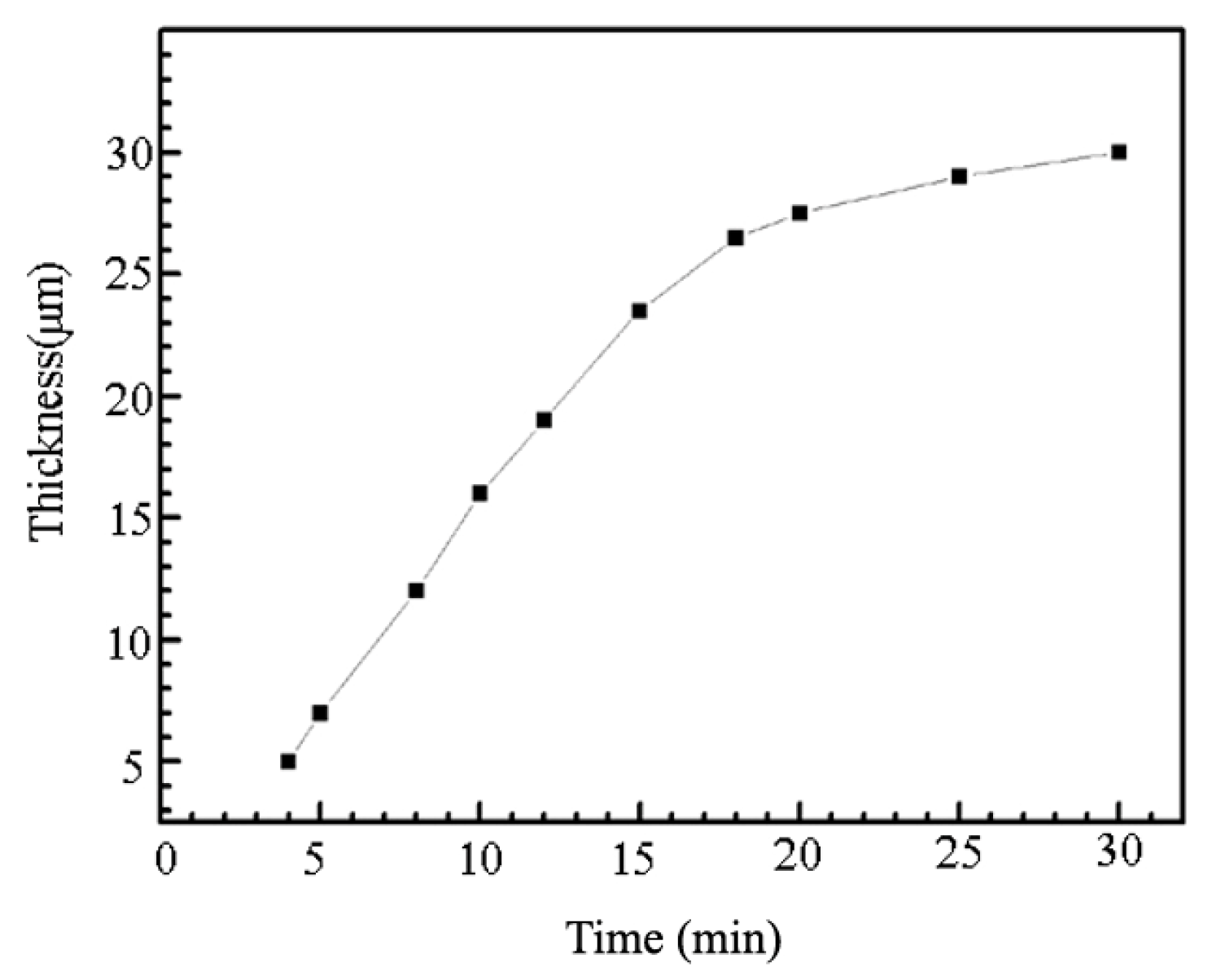
Figure 3 illustrates the correlation between the electrophoresis time and the thickness of the graphene cathode. When the electrophoresis time is less than 4 min, the thickness of the graphene cathode shows irregular changes because the graphene on the substrate surface has not yet formed a continuous graphene film at this time, as shown in Figure 2a. By increasing the electrophoresis time of the graphene cathode, the thickness of the graphene cathode increased linearly from 5 min to 15 min. After 15 min of electrophoretic deposition, the surface of the cathode was completely covered with a GS. The thickness of the GS cathode increases gradually with the further extension of electrophoresis time. It can be observed in Figure 2b that, when the electrophoresis time exceeds 20 min, the surface non-uniformity of the graphene cathode increases. This non-uniformity will impact the field emission performance of the graphene cathode. When the deposition time was 10 min, as shown in Figure 2c,d, the graphene fully covered the surface with a uniform morphology. Therefore, the graphene cathode with an electrophoresis time of 10 min was selected for the study, and it will also be utilized in subsequent experiments.
The surface morphology of the deposited GSs is shown in Figure 4. SEM images in Figure 4a,b show the pristine GSs prepared by ED. It can be found that the film has many edges that would act as emitters when subjected to an electric field. Figure 4c,d shows the morphology of the GS coated with rare earth oxides. When the ethanol solution was dropped onto a GS, it quickly dispersed on the surface due to absorption. Therefore, the rare earth nitride dissolved in ethanol spontaneously disperses well on the surface of a GS. In contrast to the CsI coated on GS with particles, the rare earth oxides form a uniform thin film after annealing. Due to its low melting temperature, CsI would melt during the thermal annealing process. When the temperature cools down, the CsI transforms into small particles on the surface of a GS. While the rare earth oxides have a very high melting temperature and excellent chemical stability, they form a continuous thin film on the surface of a GS that remains unchanged after thermal annealing. With a low work function, this uniformly covered thin film would facilitate the emission of electrons from the edges of the GS more easily, thereby enhancing the effectiveness of emission sites. Moreover, with a high melting temperature and excellent chemical stability, the coated rare earth thin film would also act as an anti-bombardment thin film and improve its field emission stability.
To verify the Gd2O3 coating on the graphene cathode surface, X-ray photoelectron spectroscopy (XPS) was used to analyze the GS cathode. The XPS analysis of the GS cathode before and after Gd2O3 coating in Figure 5 shows a strong carbon atom absorption peak near 284.7 eV. The O1s absorption peak at 532.7 eV represents the oxygen residue remaining after the reduction in graphene. The C1s absorption peak of the graphene cathode after coating with gadolinium oxide did not change significantly, while the O1s absorption peak at 532.7 eV increased. The absorption peaks of Gd3d5/2 and Gd3d3/2 appeared near 1188 eV and 1218 eV, respectively.
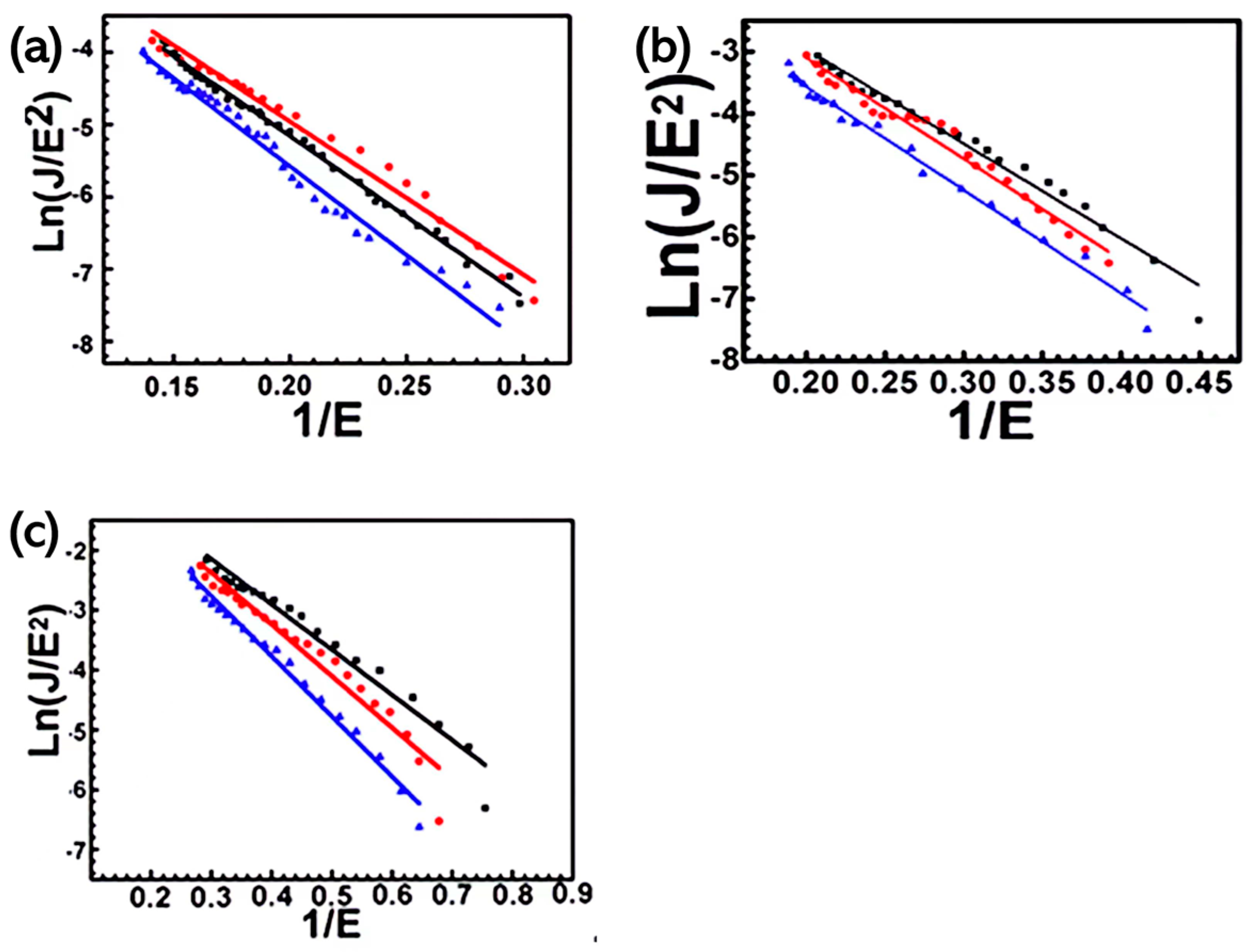
The field emission property of GSs is changeable and can be enhanced by various rare earth oxide films. Figure 6a shows the repeatable field emission tests of pristine GSs. The results indicate that the turn-on field and threshold field of a pristine GS are about 4.2 V/µm and 7.8 V/µm, Figure 7a shows the corresponding F-N curve, respectively. Figure 6b shows the field emission tests of GSs coated with La2O3, and Figure 7b shows the corresponding F-N curve. It can be observed that the field emission property is significantly enhanced after coating. The turn-on field was reduced from 4.2 V/µm to 2.2 V/µm, and the threshold field was decreased from 8 V/µm to 4.8 V/µm. As indicated in Table 1, the results of the turn-on field and threshold field were compared with those reported in other works in the literature, revealing that the GS coated with Gd2O3 in this study exhibited lower values for both the turn-on field and threshold field, except the ZnO quantum dots decoration for a GS.
Figure 6c shows the field emission of the GS coated with Gd2O3, Figure 7c shows the corresponding F-N curve. The turn-on field and threshold field of the GS coated with Gd2O3 are 1.7 V/µm and 3.4 V/µm, respectively. To compare the field emission properties, the field emission results of the rare earth oxide-coated GS and CsI-coated GS are combined in Figure 6d. It can be found that the field emission properties of GS emitters are improved after coating them with rare earth oxide films. When compared to the CsI-coated GS, the rare earth oxide-coated GS exhibits superior field emission properties. The CsI-coated GS is different from the rare earth-coated GS, which, owing to the coverage status of the GS with particles. These CsI particles would increase the local field enhancement factor. Rare earth oxides form a continuous thin film on the GS. It does not change the morphology but creates more emission sites compared to CsI particles. As a result, the field emission properties of the rare earth oxide-coated GS are better than those of CsI-coated GS.
The field emission mainly depends on the local electric field and work function. The local electric field is determined by the combination of the externally applied electric field and the field enhancement factor. It is influenced by the surface morphology. Because the rare earth oxide covered on the GS with a thin film, it would not change the surface morphology, and the corresponding field enhancement factor would not have obviously changed in experiment. According to the F-N equation, the field enhancement factor relies on the following equation:
where is the slope of the F-N curve from the field emission tests. Figure 6a shows that the field emission tests of the pristine GS after ED have good repeatable properties. Subsequently, the field enhancement factor of a pristine GS would also remain at the same level in different samples. Unlike the CsI coating on a GS, the rare earth oxide coating forms a thin film on the surface of the graphene cathode without significantly altering its field enhancement factor. Based on repeated experimental tests shown in Figure 6a, the field enhancement factor of the graphene cathode remains essentially unchanged after electrophoresis. This is consistent with the field emission F-N formula. However, the field emission properties of GS emitters were improved. Hence, here, the enhancement of the rare earth oxide coating must attribute the lower work function and resulting increment of emission sites after coating.
Field emission stability tests are shown in Figure 8. Figure 8a illustrates the stability of the pristine GS, which exhibits severe fluctuations and has a significant decline after prolonged emission. Figure 8b illustrates the emission stability of the GS coated with a La2O3 film. It initially shows little fluctuation but stabilizes after 6 h of continuous field emission, with a slight decline. When the GS is coated with Gd2O3, the field emission becomes more stable without any decline. This may be due to the low work function and anti-bombardment properties of the Gd2O3 film, which activates more emission sites on the coated GS. This allows for the sharing of emission currents and results in a more stable emission.
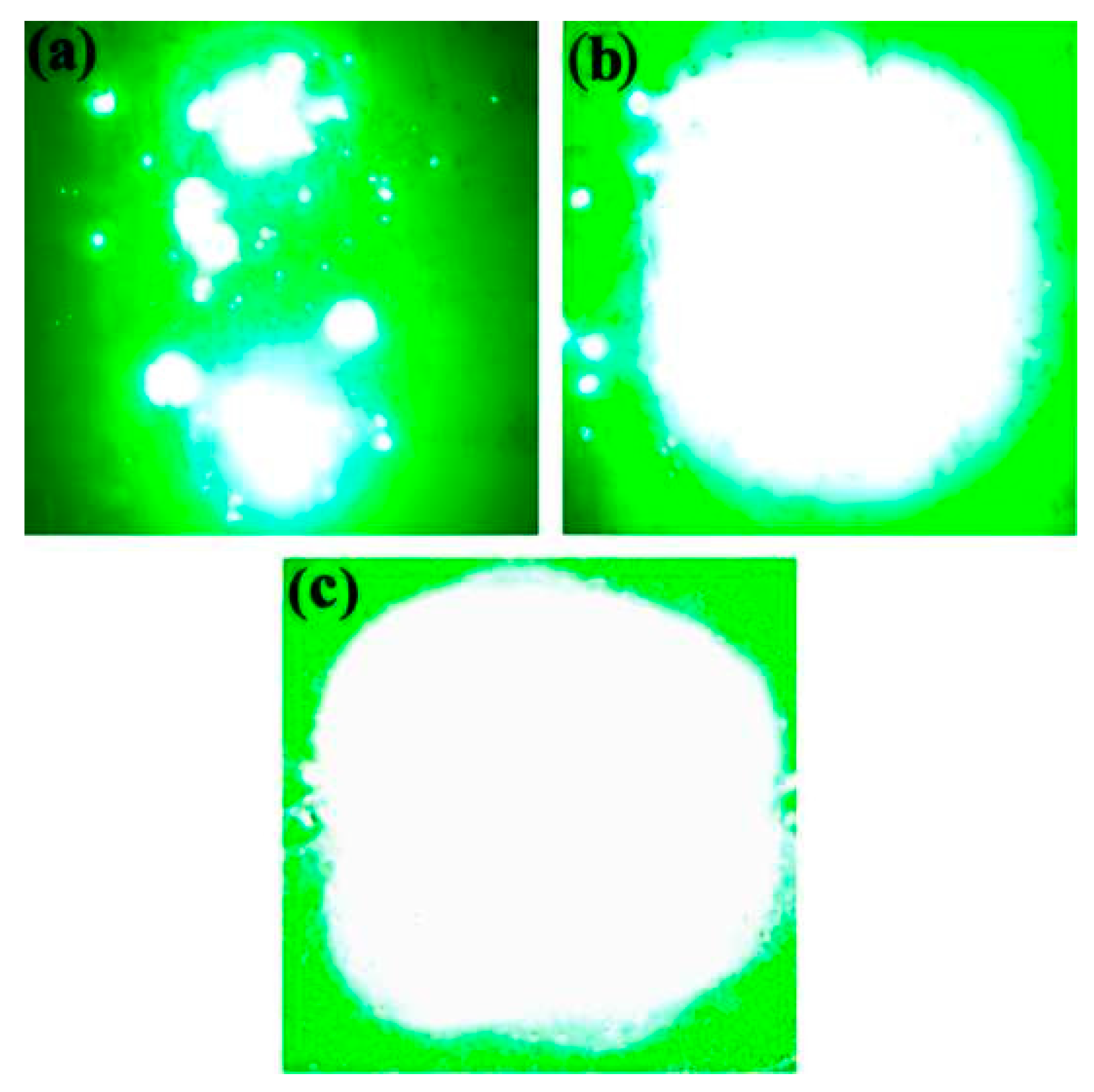
To analyze the increased emission site of GSs after coating, the field emission patterns of GSs with a size of 10 mm × 10 mm are shown in Figure 9. The field emission pattern of the pristine GS in Figure 9a shows that the GS has only a few emission sites during the field emission. These emission sites may depend on the random protrusions after ED. In Figure 9b, the emission pattern of the La2O3-coated GS is homogeneous. This may be due to the low work function of the rare earth oxide thin film, which activates more emission sites on the coated GS, leading to a more homogeneous field emission pattern. Gadolinium, as a rare earth metal, easily forms a stable oxide of gadolinium. This gadolinium oxide, like other alkali metal elements, will form a positive outward dipole moment on the surface of graphene, reducing the surface work function of the graphene cathode. Compared with lanthanum metals, gadolinium has stronger ionization energy and forms a stronger dipole moment, resulting in a more significant reduction in work function. In summary, graphene cathodes coated with gadolinium oxide on the surface will have lower work functions. Figure 9c shows the emission pattern of the Gd2O3-coated GS. With a lower surface work function, the Gd2O3-coated GS has more emission sites, leading to a more favorable emission pattern. Furthermore, the cathode will sustain damage due to prolonged electron emission, leading to significant fluctuations and a noticeable decrease in the emission current. With surface coating, the effective emission area of the GS cathode is expanded, leading to improved uniformity and enhanced stability of electron emission. Consequently, continuous emission stability can be maintained for an extended period under a specific current.
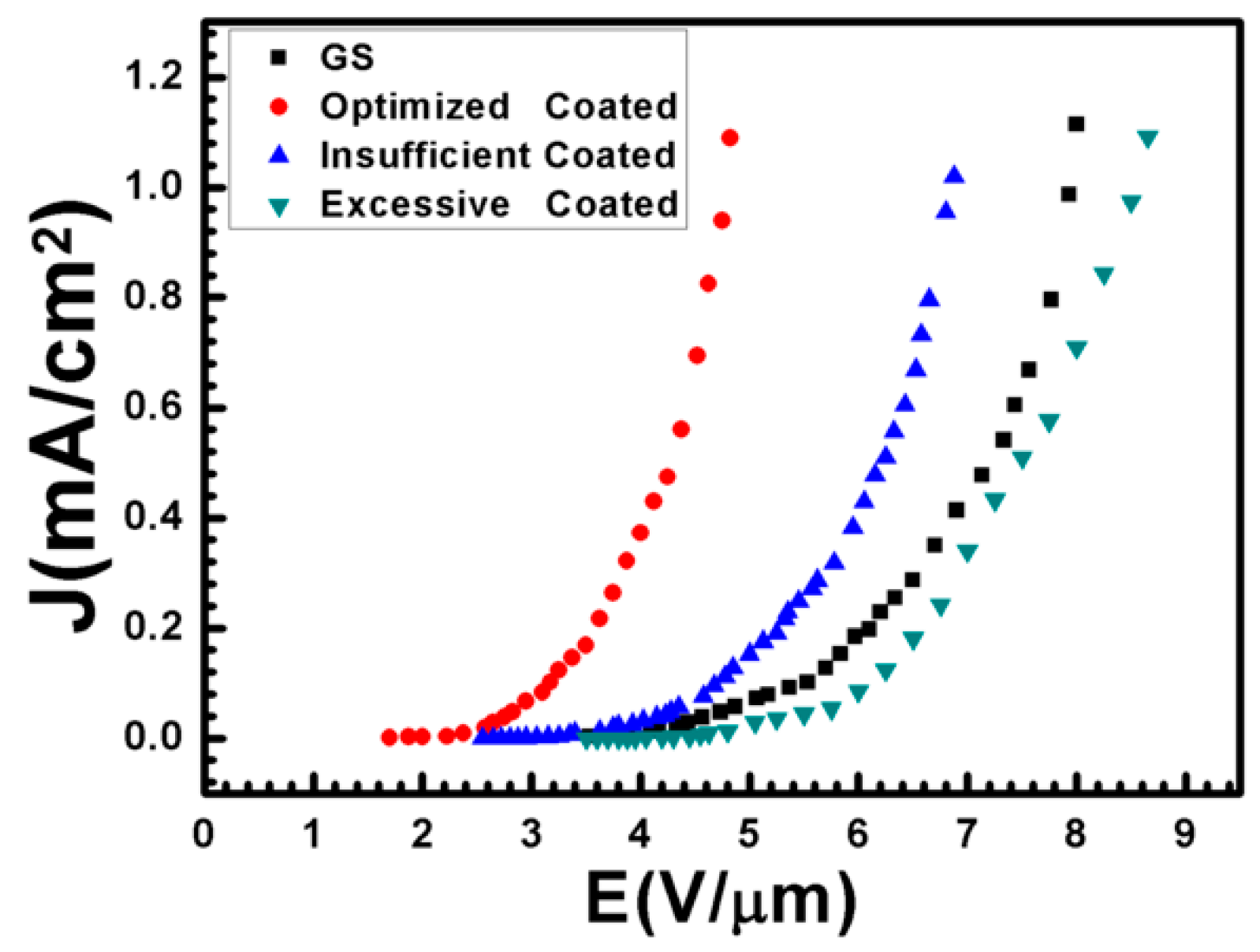
The experiment shows that the concentration of the rare earth solution significantly influences the field emission properties. Figure 10 shows the field emission results of Gd2O3-coated GS with various levels. When the GS is insufficiently coated, the field emission properties do not show significant improvement. When the concentration of Gd2O3 solution exceeds 40 mg/100 mL, the field emission of GS that is excessively coated also deteriorates. The thickness of the Gd2O3 film coating increases with the concentration. When the concentration is low, the insufficient coating does not cause a significant change in the emission sites. A thick and non-conductive rare earth oxide film can impede electron transport, leading to a deterioration in the performance of the GS field emission.
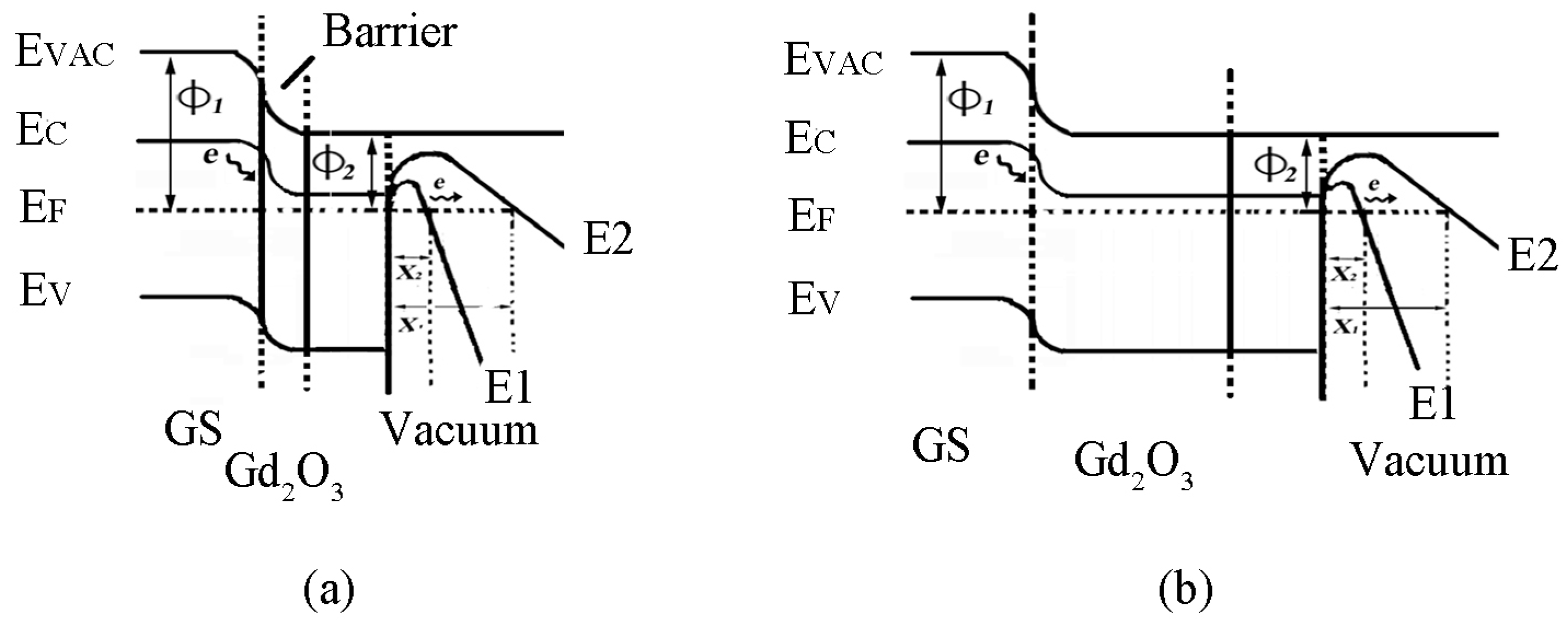
Field emission occurs when electrons tunnel out of the Fermi level in response to an externally applied electric field. When the electric field is applied, the band bends, and the width of barrier X decreases. The mechanism could be illustrated by the diagram in Figure 11. In pristine GS, as shown in Figure 11a, the high surface work function results in a higher potential barrier, X1. This necessitates a stronger applied field to lower the barrier for electron emission. In addition, the pristine GS had a higher turn-on field. When the GS is coated with a thin film of rare earth at the appropriate level, electrons can easily be transported to the surface, facilitating emission due to the low surface work function. Figure 11b shows that the potential barrier of X2 is smaller than that of X1, which would facilitate field emission. As a result, the field emission properties of GS coated with a thin layer of material are improved.
From the experimental results, there is a relatively optimized range of gadolinium oxide coating to enhance the field emission effect of GS emitter. When the concentration of gadolinium oxide solution is low, the field emission performance of the graphene cathode shows only marginal improvement. The field emission characteristics of the cathode can be greatly improved by increasing the concentration of gadolinium oxide. The field emission performance of graphene decreases when the thickness of the coating layer is further increased. Unlike cesium iodide, gadolinium oxide has a very high melting point. When gadolinium oxide is reduced by heating, the temperature required for reduction is much lower than its melting point. The decomposed gadolinium oxide does not melt; instead, it forms a uniform gadolinium oxide film on the surface of the graphene cathode.
Figure 12 shows graphene coated with gadolinium oxide with various thicknesses. When the concentration of gadolinium oxide solution is low, a continuous coating is not formed on the graphene surface, leading to the poor field emission performance of the graphene cathode. Further increasing the concentration of gadolinium oxide forms a continuous film of suitable thickness on the surface of the graphene cathode, as shown in Figure 12a. It can significantly improve the field emission characteristics of the cathode. Gadolinium oxide is a high dielectric constant medium that is often used as an insulating layer. Electron transport in gadolinium oxide coatings is challenging. When the thickness of the coating is further increased, it becomes difficult for electrons to move from the graphene cathode to the gadolinium oxide coating surface for electron emission, as shown in Figure 12b. This results in a decrease in the field emission performance of graphene.
4. Conclusions
A simple method for enhancing field emissions in GS with a low work-function rare-earth oxide coating prepared by drop coating is proposed. In order to optimize the field emission of coated graphene sheets (GSs), various rare earth oxide films were applied to coat the GSs. It was found that the field emission performance of the GSs was significantly enhanced. The experimental results demonstrate that the La2O3 and Gd2O3 coating can significantly enhance the field emission performance of GSs. The field emission performance of coated GSs can be optimized by adjusting the coating concentration of rare earth oxides. In addition, the results of the field-emission stability test and the study of the emission mechanism indicate that coating with a rare earth oxide film is more likely to enhance field emissions by generating more emission points after coating. The GS emitter deposited by industrial methods exhibit good field emission characteristics, making them suitable for use as potential field emitters.
Author Contributions
Conceptualization, B.Z.; Methodology, G.Z., Z.D. and D.W.; Validation, Z.D. and X.X.; Writing—original draft, J.L. All authors have read and agreed to the published version of the manuscript.
Funding
This work was partially supported by National Nature Science Foundation of China (Nos. 61921002 and 62131006), Fundamental Research Funds for the Central Universities, and National Key Laboratory of Science and Technology on Vacuum Electronics (No. 6142807190205).
Institutional Review Board Statement
Not applicable.
Data Availability Statement
Data are contained within the article.
Conflicts of Interest
The authors declare no conflict of interest.
References
- Milne, W.I.; Teo, K.B.K.; Amaratunga, G.A.J.; Legagneux, P.; Gangloff, L.; Schnell, J.P.; Semet, V.; Thien Binh, V.; Groening, O. Carbon nanotubes as field emission sources. J. Mater. Chem. 2004, 14, 933–943. [Google Scholar] [CrossRef]
- Yue, G.Z.; Qiu, Q.; Gao, B.; Cheng, Y.; Zhang, J.; Shimoda, H.; Chang, S.; Lu, J.P.; Zhou, O. Generation of continuous and pulsed diagnostic imaging x-ray radiation using a carbon-nanotube-based field-emission cathode. Appl. Phys. Lett. 2002, 81, 355–357. [Google Scholar] [CrossRef]
- Novoselov, K.S.; Geim, A.K.; Morozov, S.V.; Jiang, D.; Zhang, Y.; Dubonos, S.V.; Grigorieva, I.V.; Firsov, A.A. Electric field effect in atomically thin carbon films. Science 2004, 306, 666–669. [Google Scholar] [CrossRef] [PubMed]
- Geim, A.K. Graphene: Status and Prospects. Science 2009, 324, 1530–1534. [Google Scholar] [CrossRef]
- Zhu, Y.W.; Murali, S.; Stoller, M.D.; Ganesh, K.J.; Cai, W.W.; Ferreira, P.J.; Pirkle, A.; Wallace, R.M.; Cychosz, K.A.; Thommes, M.; et al. Carbon-Based Supercapacitors Produced by Activation of Graphene. Science 2011, 332, 1537–1541. [Google Scholar] [CrossRef] [PubMed]
- Malesevic, A.; Kemps, R.; Vanhulsel, A.; Chowdhury, M.P.; Volodin, A.; Van Haesendonck, C. Field emission from vertically aligned few-layer graphene. J. Appl. Phys. 2008, 104, 084301. [Google Scholar] [CrossRef]
- Krivchenko, V.A.; Pilevsky, A.A.; Rakhimov, A.T.; Seleznev, B.V.; Suetin, N.V.; Timofeyev, M.A.; Bespalov, A.V.; Golikova, O.L. Nanocrystalline graphite: Promising material for high current field emission cathodes. J. Appl. Phys. 2010, 107, 014315. [Google Scholar] [CrossRef]
- Yamaguchi, H.; Murakami, K.; Eda, G.; Fujita, T.; Guan, P.; Wang, W.; Gong, C.; Boisse, J.; Miller, S.; Acik, M.; et al. Field Emission from Atomically Thin Edges of Reduced Graphene Oxide. ACS Nano 2011, 5, 4945–4952. [Google Scholar] [CrossRef] [PubMed]
- Hummers, W.S., Jr.; Offeman, R.E. Preparation of Graphitic Oxide. J. Am. Chem. Soc. 1958, 80, 1339. [Google Scholar] [CrossRef]
- Dikin, D.A.; Stankovich, S.; Zimney, E.J.; Piner, R.D.; Dommett, G.H.B.; Evmenenko, G.; Nguyen, S.T.; Ruoff, R.S. Preparation and characterization of graphene oxide paper. Nature 2007, 448, 457–460. [Google Scholar] [CrossRef] [PubMed]
- Liu, J.L.; Zeng, B.Q.; Wu, Z.; Sun, H. Enhanced Field Electron Emission of Graphene Sheets by CsI Coating after Electrophoretic Deposition. ACS Appl. Mater. Interfaces 2012, 4, 1219–1224. [Google Scholar] [CrossRef]
- Wu, Z.; Pei, S.; Ren, W.; Tang, D.; Cheng, H. Field Emission of Single-Layer Graphene Films Prepared by Electrophoretic Deposition. Adv. Mater. 2009, 21, 1756. [Google Scholar] [CrossRef]
- Su, W.S.; Leung, T.C.; Chan, C.T. Work function of single-walled and multiwalled carbon nanotubes: First-principles study. Phys. Rev. B 2007, 76, 235413. [Google Scholar] [CrossRef]
- Ramprasad, R.; von Allmen, P.; Fonseca, L.R.C. Contributions to the work function: A density-functional study of adsorbates at graphene ribbon edges. Phys. Rev. B 1999, 60, 6023–6027. [Google Scholar] [CrossRef]
- Sinsarp, A.; Yamada, Y.; Sasaki, M.; Yamamoto, S. Microscopic study on the work function reduction induced by Cs-adsorption. Jpn. J. Appl. Phys. Part 1-Regul. Pap. Brief Commun. Rev. Pap. 2003, 42, 4882–4886. [Google Scholar] [CrossRef]
- Yamada, Y.; Sinsarp, A.; Sasaki, M.; Yamamoto, S. Scanning tunneling microscopy (STM)/local tunnneling barrier height (LBH) studies on Cs adsorption on a Pt(111) surface. Jpn. J. Appl. Phys. Part 1-Regul. Pap. Short Notes Rev. Pap. 2002, 41, 5003–5007. [Google Scholar] [CrossRef]
- Liu, J.L.; Jiang, R.R.; Yang, K.Q.; Chai, X.; Fang, Y.; Deng, J.; Liu, X.C.; Zeng, B.Q. Performance of screen-printed large lateral size single-layer graphene emitter with buffer layer. Mater. Lett. 2018, 229, 232–235. [Google Scholar] [CrossRef]
- Vlahos, V.; Booske, J.H.; Morgan, D. Ab initio study of the effects of thin CsI coatings on the work function of graphite cathodes. Appl. Phys. Lett. 2007, 91, 144102. [Google Scholar] [CrossRef]
- Vlahos, V.; Morgan, D.; LaCour, M.; Golby, K.; Shiffler, D.; Booske, J.H. Surface chemical analysis and ab initio investigations of CsI coated C fiber cathodes for high power microwave sources. J. Appl. Phys. 2010, 107, 044903. [Google Scholar] [CrossRef]
- Lee, J.; Park, J.; Kim, J.; Yi, W. Effect of double layer coating on carbon nanotubes for field emission and secondary electron emission measurement. J. Vac. Sci. Technol. B 2007, 25, 570–574. [Google Scholar] [CrossRef]
- Baby, T.T.; Ramaprabhu, S. Cold field emission from hydrogen exfoliated graphene composites. Appl. Phys. Lett. 2011, 98, 183111. [Google Scholar] [CrossRef]
- Kumari, M.; Gautam, S.; Shah, P.V.; Pal, S.; Ojha, U.S.; Kumar, A.; Naik, A.A.; Rawat, J.S.; Chaudhury, P.K.; Harsh; et al. Improving the field emission of carbon nanotubes by lanthanum-hexaboride nano-particles decoration. Appl. Phys. Lett. 2012, 101, 123116. [Google Scholar] [CrossRef]
- Michaelson, H.B. The work function of the elements and its periodicity. J. Appl. Phys. 1977, 48, 4729. [Google Scholar] [CrossRef]
- Wang, J.S.; Li, H.Y.; Yang, S.; Liu, Y.Q.; Zhou, M.L. Study on rare earth oxide-molybdenum cermet cathode materials. J. Alloys Compd. 2004, 385, 288–293. [Google Scholar] [CrossRef]
- Lee, S.; Liao, X.-H.; Liu, G.-Q. Rare Earth Metal Compounds as Thermionic Cathode Material. Acta Electron. Sin. 1965, 1, 48–56. [Google Scholar]
- Robertson, J.; Falabretti, B. Band offsets of high K gate oxides on III-V semiconductors. J. Appl. Phys. 2006, 100, 014111. [Google Scholar] [CrossRef]
- Li, Y.-L.; Chen, N.-F.; Zhou, J.-P.; Song, S.-L.; Liu, L.-F.; Yin, Z.-G.; Cai, C.-L. Effect of the oxygen concentration on the properties of Gd2O3 thin films. J. Cryst. Growth 2004, 265, 548–552. [Google Scholar] [CrossRef]
- Chen, T.; Baoqing, Z.; Liu, J.L.; Dong, J.H.; Liu, X.Q.; Wu, Z.; Yang, X.Z.; Li, Z.M. High throughput exfoliation of graphene oxide from expanded graphite with assistance of strong oxidant in modified Hummers method. J. Phys. Conf. Ser. 2009, 188, 012051. [Google Scholar] [CrossRef]
- Li, Z.; Yang, B.; Yun, G.; Zhang, S.; Zhang, M.; Zhao, M. Synthesis of Sn nanoparticle decorated graphene sheets for enhanced field emission properties. J. Alloys Compd. 2013, 550, 353–357. [Google Scholar] [CrossRef]
- Sun, L.; Zhou, X.; Lin, Z.; Guo, T.; Zhang, Y.; Zeng, Y. Effects of ZnO Quantum Dots Decoration on the Field Emission Behavior of Graphene. ACS Appl. Mater. Interfaces 2016, 8, 31856–31862. [Google Scholar] [CrossRef] [PubMed]
- Rout, C.S.; Joshi, P.D.; Kashid, R.V.; Joag, D.S.; More, M.A.; Simbeck, A.J.; Washington, M.; Nayak, S.K.; Late, D.J. Enhanced field emission properties of doped graphene nanosheets with layered SnS2. Appl. Phys. Lett. 2014, 105, 043109. [Google Scholar] [CrossRef]
- Sreekanth, M.; Ghosh, S.; Biswas, P.; Kumar, S.; Srivastava, P. Improved field emission from indium decorated multi-walled carbon nanotubes. Appl. Surf. Sci. 2016, 383, 84–89. [Google Scholar] [CrossRef]
Figure 1.
AFM image of a GS.

Figure 2.
SEM of graphene cathode at different electrophoretic times: (a) 2 min, (b) 20 min, and (c) 10 min. (d) A high-resolution image of (c).
Figure 2.
SEM of graphene cathode at different electrophoretic times: (a) 2 min, (b) 20 min, and (c) 10 min. (d) A high-resolution image of (c).

Figure 3.
Relationship between graphene cathode thickness and electrophoresis time.

Figure 4.
Scanning electron microscopy of deposited GS emitters: (a,b) pristine GS and (c,d) GS coated with rare earth oxide film.
Figure 4.
Scanning electron microscopy of deposited GS emitters: (a,b) pristine GS and (c,d) GS coated with rare earth oxide film.

Figure 5.
(a) XPS analysis of GS cathode before and after gadolinium oxide coating. (b) High-resolution XPS spectrum of Gd 3d5/2 and Gd 3d3/2.
Figure 5.
(a) XPS analysis of GS cathode before and after gadolinium oxide coating. (b) High-resolution XPS spectrum of Gd 3d5/2 and Gd 3d3/2.

Figure 6.
Field emission curves of GSs. (a) Repeatable tests of pristine GS. (b) Repeatable tests of La2O3-coated GS. (c) Repeatable tests of Gd2O3-coated GS. (d) Combination of field emission from GSs before and after coating.
Figure 6.
Field emission curves of GSs. (a) Repeatable tests of pristine GS. (b) Repeatable tests of La2O3-coated GS. (c) Repeatable tests of Gd2O3-coated GS. (d) Combination of field emission from GSs before and after coating.

Figure 7.
F-N curves of GSs. (a) Repeatable tests of pristine GS. (b) Repeatable tests of La2O3−coated GS. (c) Repeatable tests of Gd2O3−coated GS.
Figure 7.
F-N curves of GSs. (a) Repeatable tests of pristine GS. (b) Repeatable tests of La2O3−coated GS. (c) Repeatable tests of Gd2O3−coated GS.

Figure 8.
Field emission stability tests of GS: (a) the stability test of pristine GS after ED, (b) stability test of GS coated with La2O3, and (c) stability test of GS coated with Gd2O3.
Figure 8.
Field emission stability tests of GS: (a) the stability test of pristine GS after ED, (b) stability test of GS coated with La2O3, and (c) stability test of GS coated with Gd2O3.

Figure 9.
Field emission pattern of GS emitters with size of 10 mm × 10 mm. (a) Field emission pattern of pristine GS after ED. (b) Field emission pattern of GS coated with La2O3. (c) Field emission pattern of GS coated with Gd2O3.
Figure 9.
Field emission pattern of GS emitters with size of 10 mm × 10 mm. (a) Field emission pattern of pristine GS after ED. (b) Field emission pattern of GS coated with La2O3. (c) Field emission pattern of GS coated with Gd2O3.

Figure 10.
Field emission of GS emitters coated with different concentrations of Gd2O3 solution.

Figure 11.
Field emission scheme of GS coated with rare earth oxide. (a) Field emission from GS after ED. (b) Field emission from rare earth-coated GS.
Figure 11.
Field emission scheme of GS coated with rare earth oxide. (a) Field emission from GS after ED. (b) Field emission from rare earth-coated GS.

Figure 12.
Graphene-coated cathodes with gadolinium oxide of different thicknesses: (a) thin gadolinium oxide coating and (b) thick gadolinium oxide coating.
Figure 12.
Graphene-coated cathodes with gadolinium oxide of different thicknesses: (a) thin gadolinium oxide coating and (b) thick gadolinium oxide coating.


Table 1.
Comparison of the turn-on fields and threshold fields of Gd2O3-coated graphene, with results from other references.
Table 1.
Comparison of the turn-on fields and threshold fields of Gd2O3-coated graphene, with results from other references.
| Turn-on Field | Threshold field | Ref. | |
|---|---|---|---|
| Present work | 1.7 V/μm (10 μA/cm2) | 3.4 V/μm (1 mA/cm2) | |
| Gs Coating CsI | 2.5 V/μm (10 μA/cm2) | 3.1 V/μm (1 mA/cm2) | [11] |
| SnO2/graphene | 4.14 V/μm (1 μA/cm2) | 9.4 V/μm (1 mA/cm2) | [29] |
| ZnO quantum dots decoration | 0.9 V/μm (10 μA/cm2) | 2.6 V/μm (1 mA/cm2) | [30] |
| Graphene with layered SnS2 | 2.65 V/μm (10 μA/cm2) | 3.2 V/μm (300 μA/cm2) | [31] |
| In/Carbon nanotube | 2.0 V/μm (10 μA/cm2) | 3.9 V/μm (1 mA/cm2) | [32] |
Disclaimer/Publisher’s Note: The statements, opinions and data contained in all publications are solely those of the individual author(s) and contributor(s) and not of MDPI and/or the editor(s). MDPI and/or the editor(s) disclaim responsibility for any injury to people or property resulting from any ideas, methods, instructions or products referred to in the content. |
© 2024 by the authors. Licensee MDPI, Basel, Switzerland. This article is an open access article distributed under the terms and conditions of the Creative Commons Attribution (CC BY) license (https://creativecommons.org/licenses/by/4.0/).
Share and Cite
MDPI and ACS Style
Dong, Z.; Liu, J.; Wang, D.; Zhong, G.; Xiang, X.; Zeng, B. Optimized Field Emission from Graphene Sheets with Rare Earth Oxides. Coatings 2024, 14, 545. https://doi.org/10.3390/coatings14050545
AMA Style
Dong Z, Liu J, Wang D, Zhong G, Xiang X, Zeng B. Optimized Field Emission from Graphene Sheets with Rare Earth Oxides. Coatings. 2024; 14(5):545. https://doi.org/10.3390/coatings14050545
Chicago/Turabian StyleDong, ZhiJianMuCuo, Jianlong Liu, Dayang Wang, Guoling Zhong, Xingyue Xiang, and Baoqing Zeng. 2024. "Optimized Field Emission from Graphene Sheets with Rare Earth Oxides" Coatings 14, no. 5: 545. https://doi.org/10.3390/coatings14050545
Note that from the first issue of 2016, this journal uses article numbers instead of page numbers. See further details here.