Article

AZO Thin Films by Sol-Gel Process for Integrated Optics

1
Laboratory of Sciences of Processes and Materials (LSPM), CNRS-UPR 3407, Paris 13 University, Sorbonne Paris Cité, 99-Jean-Baptiste Clément Avenue, Villetaneuse 93430, France
2
Laboratory of Semiconductors, University of Badji Mokhtar, BP 12, Annaba 23000, Algeria
3
Lasers Physics Laboratory (LPL), CNRS-UMR 7538, Paris 13 University, Sorbonne Paris Cité, 99-Jean-Baptiste Clément Avenue, Villetaneuse 93430, France
*
Author to whom correspondence should be addressed.
Coatings 2013, 3(3), 126-139; https://doi.org/10.3390/coatings3030126
Submission received: 25 May 2013 / Revised: 26 June 2013 / Accepted: 26 June 2013 / Published: 3 July 2013

Abstract

:
Undoped and aluminum-doped zinc oxide (AZO) thin films are prepared by the sol-gel process. Zinc acetate dihydrate, ethanol, and monoethanolamine are used as precursor, solvent, and stabilizer, respectively. In the case of AZO, aluminum nitrate nonahydrate is added to the precursor solution with an atomic percentage equal to 1 and 2 at.% Al. The multi thin layers are deposited by spin-coating onto glass substrates, and are transformed into ZnO upon annealing at 550 °C. Films display a strong preferential orientation, with high values for the Texture Coefficients (TC) of the (002) direction (TC(002) ≈ 3). The structural, morphological, and optical properties of the thin films as a function of aluminum content have been investigated using X-Ray Diffraction (XRD), Atomic Force Microscopy (AFM), and Scanning Electronic Microscopy (SEM). Waveguiding properties of the thin films have been also studied using m-lines spectroscopy. The results indicate that the films are monomodes at 632.8 nm with optical propagation optical losses estimated around 1.6 decibel per cm (dB/cm).

1. Introduction

Zinc oxide (ZnO) is a II-VI group semiconductor and usually adopts a hexagonal wurtzite crystal structure [1,2,3,4]. It has distinct advantages over other competitors, e.g., abundance in earth crust, non-toxicity, low material costs, chemical stability, high transparency in the visible and near infrared spectral region, etc. [1,3]. It is a direct wide band gap semiconductor (Eg = 3.37 eV at 300 K) [2,3,4,5,6,7] with a similar crystal structure to gallium nitride (GaN), another wide gap semiconductor (Eg = 3.3 eV at 300 K) [2,8] and, from this direct wide band-gap comes a wide interest in its prospects in optoelectronic applications. For some of these, the interest in ZnO overlaps with that of GaN, which is widely used for production of green, blue-ultraviolet, and white light-emitting devices and lasers [7,8,9]. However, ZnO has some advantages over GaN, among which are the availability of fairly high quality ZnO bulk single crystals [8] and a large exciton binding energy (ZnO: Eex = 60 meV, GaN: Eex ~ 18-28 meV) [2]. On the other hand, ZnO has been investigated intensively due to its unique characteristics that may enable its efficient utilization in/as: varistors, piezoelectric devices such as surface-acoustic wave (SAW) and piezoelectric sensors, transparent conducting oxide (e.g., electrode of solar cells), antireflection coatings, field-effect transistors, phosphors (green phosphors in displays), chemical and biological sensors, gas sensors in electronic noses, etc. [1,5,7,9]. Furthermore, because of its transparency, its electro-optical and elasto-optical properties, ZnO is attractive for integrated photonic devices [5,9].
Undoped and doped ZnO thin films have been made by a variety of methods, among which electro-deposition [9,10], aqueous solutions [9,11], chemical bath deposition (CBD) [12], successive chemical solution deposition (SCSD) [5,6], chemical vapor deposition (CVD) [9], plasma enhanced CVD (PECVD) [13], single-source CVD (SSCVD) [14], metalorganic CVD (MOCVD) [9,15], pulsed laser deposition (PLD) [15], molecular beam epitaxy (MBE) [15], RF or DC magnetron sputtering [15,16,17], thermal oxidation of zinc or ZnS [18,19], spray pyrolysis [20], and atomic layer deposition (ALD) [21]. In addition to these methods, the sol-gel process reflects distinct advantages due to its excellent compositional control, homogeneity on the molecular level, simplicity, low cost, performing well in atmospheric pressure without the need for expensive vacuum equipment, lower crystallization temperature, and it can be used to deposit films over a large area with a very uniform thickness [3,4,22,23]. It has been used to synthesize thin films of undoped ZnO [22,23,24,25,26,27,28,29,30], Al-doped ZnO [3,4,31,32,33,34,35,36,37,38,39], and ZnO doped with other elements [36,40,41,42,43,44].
Doping in ZnO with selective elements is the effective alternative to modify its electrical, optical, magnetic, and chemical-sensing properties [9,44]. For example, transition metals (Sc, Ti, V, Cr, Mn, Fe, Co, Ni, Cu) and rare earth elements (Eu, Gd, Er) have been used as magnetic atoms in diluted magnetic semiconductors (DMS) materials for their application in “spintronic” devices [8,45].
ZnO can be an n-type and a p-type semiconductor determined by the dopant nature [4,8]. n-Type doping of ZnO is relatively easy compared to p-type doping [8] and reproducible p-type conductivity in ZnO is still a challenge [2]. However, p-type doping in ZnO may be possible by substituting either group-I elements (Li, Na, K, etc.) for Zn-atoms or group-V elements (N, P, As, Sb, etc.), and for O-atoms [1,2,4,8].
For n-type [2,3,4,7,8,39], doping with group-III elements (B, Al, Ga, In), as substitutional elements for Zn, has been attempted by many groups, resulting in high-quality, optically transparent, and highly conductive ZnO films as this substitution of divalent Zn2+ by a trivalent ion generates an excessive free electron. Especially, Al-doped ZnO (AZO) thin films have attracted a considerable amount of interest due to their good electrical conductivity with reasonably low optical loss [46].
On the other hand, n-type semiconductors may also be synthesized by substituting O-atoms by group-VII elements (F, Cl, I) [8].
The optical constants of the semiconductors play an important role, both from a fundamental and a technological viewpoint [30]. Refractive index is one of the fundamental properties for an optical material, because it is closely related to the electronic polarizability of the ions and to the local field inside materials. The evaluation of refractive indices of optical materials is highly important for applications in integrated optic devices, such as switches, filters, modulators, etc., where refractive indices are the key constants for device design [29,30,41,42]. With a refractive index of about 1.9, ZnO allows the fabrication of waveguiding layers of high transparency from the near UV to middle infrared spectral range.
In this work, our aim is to synthesize by sol-gel process ZnO thin films for integrated optics; in this framework, using Al-doping as a process parameter, we are trying to find the best compromise to obtain a material with a high refractive index and a low roughness. In order to have a thickness sufficient to observe a transmission of the signal in the thin film, as observed through m-line spectroscopy, the synthesized films were realized through the deposition of seven successive layers.
Structural, morphological, and optical properties of undoped and Al-doped ZnO thin film spin-coated on glass substrates were investigated. We report guided modes spectra for both transverse electric (TE) and transverse magnetic (TM) polarization in undoped and Al-doped ZnO waveguides. From angular spectra modes, we have measured effective indices, which permit to determine ordinary and extraordinary refractive indices of the thin films. Propagation losses measurement of the thin films have been also carried out.

2. Experimental Section

ZnO thin films were prepared by the sol-gel process. As a starting material, zinc acetate dihydrate (Zn(CH3COO)2 2H2O) was dissolved in a mixture of absolute ethanol and monoethanolamine (MEA) yielding to a precursor concentration of 0.75 mol L−1. MEA acts, at the same time, as a base and a complexing agent and the MEA to zinc acetate molar ratio was set to 2. For doped films, aluminum nitrate nonahydrate (Al(NO3)3 9H2O) was added to the mixture with an atomic percentage fixed at 1 or 2 at.% Al. The precursor solution was deposited on glass substrates by spin-coating (3000 rpm, 30 s). Synthesized films, doped and undoped, were preheated at 300 °C for 10 min after each coating. This procedure was repeated seven times to increase the thickness. The films were subsequently heated up to 550 °C for 2 h in order to obtain crystallized ZnO.
The samples were characterized by X-Ray Diffraction (XRD) using an Inel G3000 diffractometer, with a copper anode, monochromated using a Ge single crystal monochromator (CuKα1: 1.54056 Å). Using a grazing incidence with the ω angle equal to 1°, detection angles ranged from 2θ = 20° to 110° using a curved detector, having a 50 cm radius, and a 90° aperture in the asymmetrical Bragg-Brentano geometry. Scanning Electronic Microscopy (SEM) was performed using a Leica S440 microscope, Atomic Force Microscopy (AFM) by a Veeco Nanoscope DIM3, and m-lines spectroscopy [47].

3. Results and Discussion

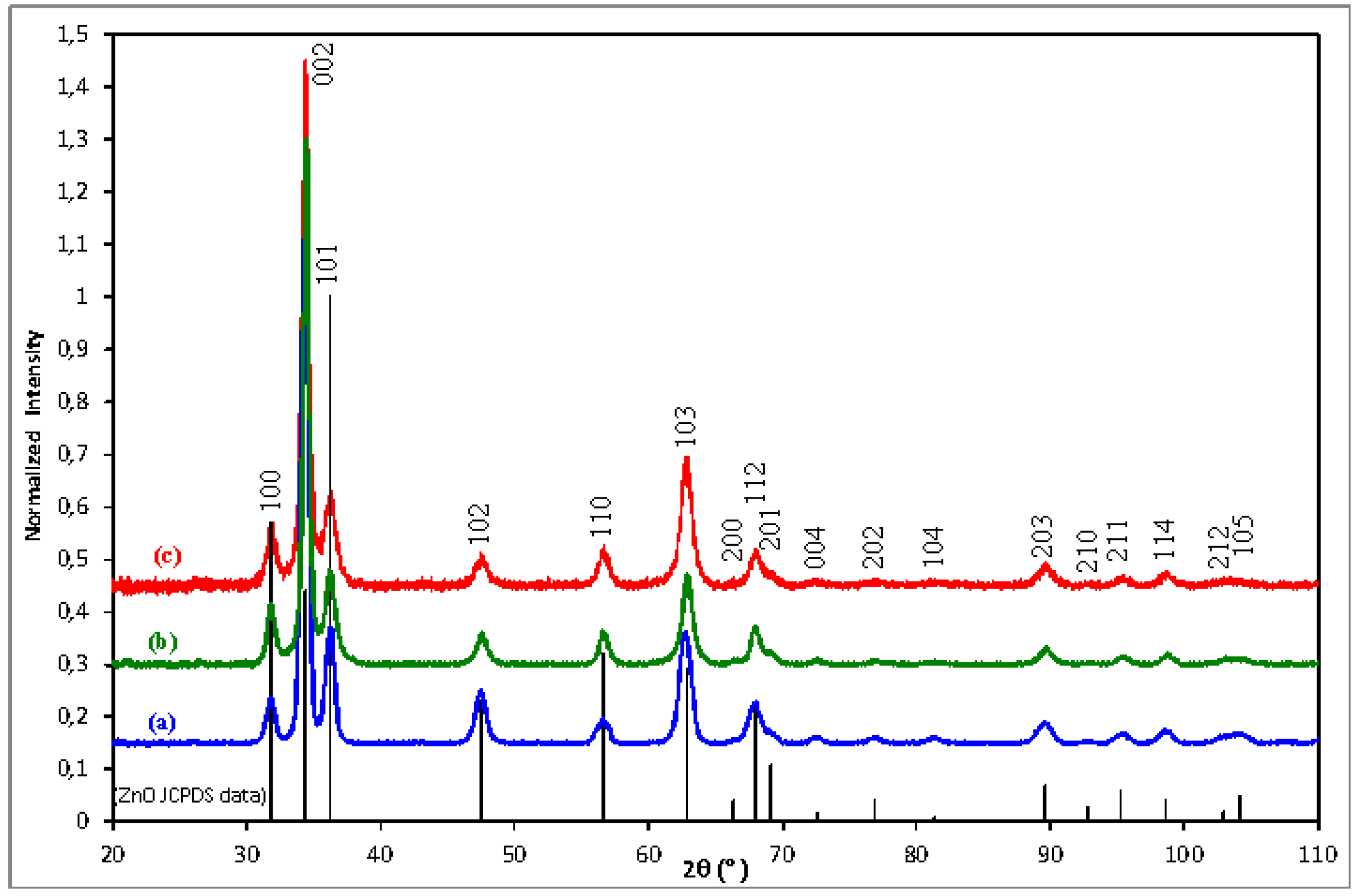
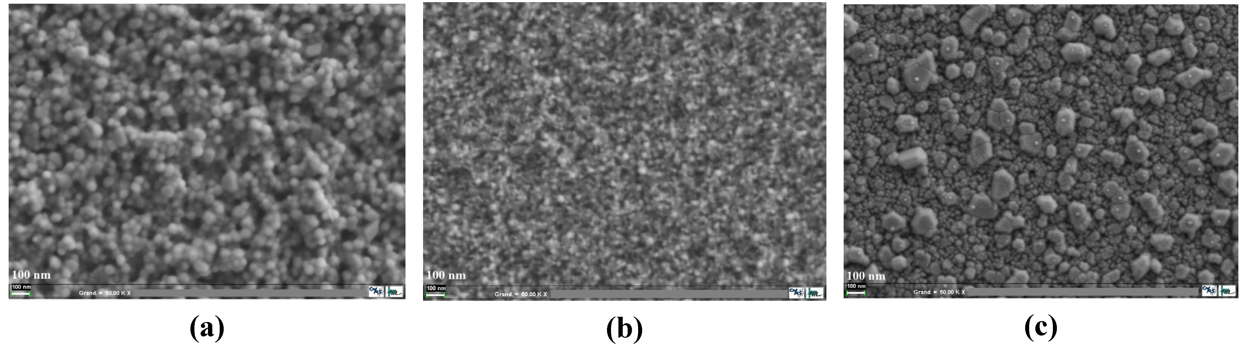
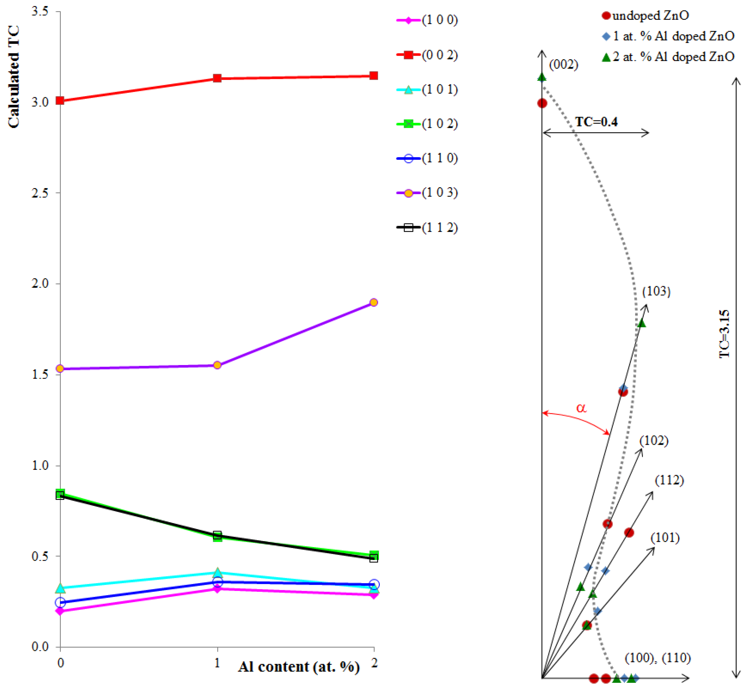
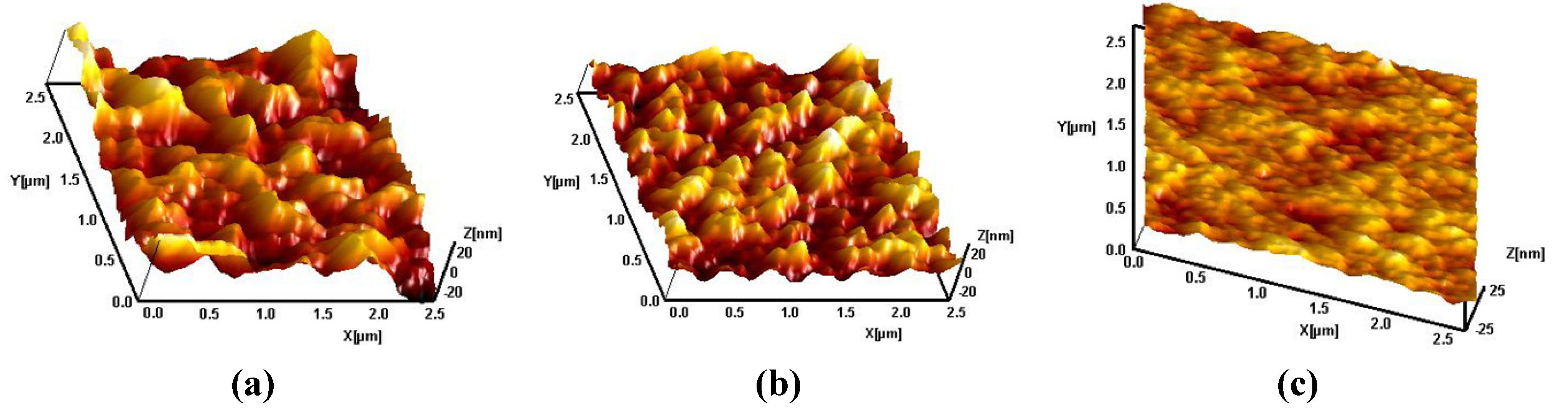
3.1. Microstructural Characterizations

Figure 1 represents the normalized diffraction patterns for the undoped, 1 at.% Al-doped and 2 at.% Al-doped 7-layer ZnO samples after removing the patterns’ baseline. Together, with these diffraction patterns, is represented the theoretical powder diffraction ZnO pattern from the JCPDS-ICDD card #36-1451 (wurtzite hexagonal structure with a = 3.2498 Å, c = 5.2066 Å). All peaks shown on this figure are identified as belonging to this card, and no other crystallized phases (e.g., Al2O3) are observed. The film patterns clearly show an over-expression of the (002) peak (i.e., parallel to the c-axis) when compared to the theoretical pattern; a similar behavior was already observed by other authors [33,34,40,48].
Figure 1. X-Ray Diffraction (XRD) patterns of 7-layer zinc oxide (ZnO) thin films obtained with an incident angle of 1°: (a) undoped, (b) 1 at.% Al-doped, (c) 2 at.% Al-doped.
Coatings 03 00126 g001
To quantify this effect, the surface areas of each peak were measured using the Fityk® program [49]. Texture coefficients (TC) were calculated using the 36–1451 JCPDS-ICDD card, giving relative intensities of 57, 44, 100, 23, 32, 29, and 23 for the (100), (002), (101), (102), (110), (103), and (112) peak, respectively. The equation giving the texture coefficient is taken from [50]:
Coatings 03 00126 i001
where Imeas. are the measured intensities of each (hkl) peak, I0 is the theoretical relative intensity, provided by the JCPDS-ICDD card, and N is the number of reflections considered. In our case N = 7, as we selected the seven most intense reflections, i.e., the (100), (002), (101), (102), (110), (103), and (112) peaks. Therefore, for an extremely textured sample, one of the TChkl would be equal to 7 while the others would be equal to 0; inversely, a fully randomly oriented sample would have a TChkl value equal to 1 for each peak.
Table 1 provides the calculated TC values of the 7 main peaks. All three samples display a similar behavior, with TC(002) above 3, TC(103) in the 1.5–1.9 range, and all the other TChkl being under 1.
Table 1. Calculated Texture Coefficients of 7-layer ZnO thin films for the 7 main peaks.
SampleDiffraction peaks
(100)(002)(101)(102)(110)(103)(112)
Undoped ZnO0.2003.0090.3270.8490.2481.5330.834
1 at.% Al-doped ZnO 0.3223.1320.4130.6070.3621.5500.614
2 at.% Al-doped ZnO 0.2903.1460.3270.5050.3471.8990.486
Figure 2-left represents the TC values as a function of Al content. Whereas TC(002) does not increase significantly, TC(103) increases sharply when Al content varies from 1 to 2 at.%. In the meantime, TC(102) and TC(112) decrease regularly from 0.83–0.85 to 0.48–0.50, while TC(100), TC(101), and TC(110) have always the smallest values, in the 0.2–0.42 range. A similar result, based only on the three main peaks was already mentioned in [33,34].
Figure 2. Texture Coefficients of 7-layer ZnO thin films calculated from the XRD patterns presented in Figure 1. Left: Texture coefficient (TC) values of the 7 main peaks of the diffraction pattern as a function of Al-doping content; Right: TC values represented in polar coordinates as a function of the α angle between the considered reflection and the (002) peak.
Coatings 03 00126 g002
Figure 2-right represents in polar coordinates the TC values as a function of the angle α between the considered diffracting plane and the (002) one. Using the lattice parameters given in the JCPDS-ICDD card (a = 3.25 Å, c = 5.2 Å), using simple 3D geometry in the hexagonal lattice, the considered angles are α(002) = 0°, α(103) = 11.753°, α(102) = 17.332°, α(112) = 23.814°, α(101) = 31.971°, and α(100) = α(110) = 90°. The curve representing TC in radius as a function of α depicts a “fish-shaped” curve. The values of the TC parameters and their evolution are thus directly correlated to the angle between the two directions: roughly speaking, the intensities of the (002) and (103) peaks, with the lower α value have the highest values and a positive slope, whereas the other peaks have values below 1 and a negative slope. This behavior indicates that increasing the Al content increases the texture of the material.
Figure 3 represents the SEM observation of the 7-layer ZnO films. The undoped film, Figure 3a, can be described as a structure of very fine particles, with a mean diameter around 60 nm, but this structure is not completely flat and looks wrinkled. For the 1 at.% Al-doped sample, Figure 3b, the sample presents an even finer microstructure, with a mean diameter around 30 nm; due to the finer particles, the surface looks flatter. Finally, the 2 at.% Al-doped sample, Figure 3c, clearly show a bimodal structure with large particles in the 50–150 nm range around which and on which much finer nanoparticles can be observed, with a mean diameter around 20 nm. The particle sizes observed by SEM are in good agreement with the calculated sizes determined by the Williamson-Hall method [51,52], using the peak broadening observed on the XRD patterns after removing the instrumental contribution, thus indicating that the SEM-observed particles are monocrystalline. This method consist in the representation of βcos(θ) as a function of sin(θ), where θ is the diffraction angle, and β the peak broadening. The slope of the given straight line yields the microstrain level, whereas the ordinate at the origin y0 yields the size of the particles ø through the formula: ø = 0.9 λ/y0, λ being the wavelength of the diffraction apparatus. Note that if the microstrain is neglected (slope = 0), the result is the same as the Sherrer method, but is more precise in the case where microstrain cannot be neglected. This method yields mean size values of 51, 26, and 19 nm for the undoped, 1 at.% Al-doped and 2 at.% Al-doped samples, respectively.
Figure 3. SEM images of 7-layer ZnO thin films: (a) undoped, (b) 1 at.% Al-doped, (c) 2 at.% Al-doped.
Coatings 03 00126 g003
SEM observations and Williamson-Hall calculations show that the particle size decreases with Al content. Indeed, aluminum having a smaller ionic radius than zinc (rZn2+ = 0.074 nm and rAl3+ = 0.054 nm) [3,36], particles forming a matrix become smaller with increased doping concentration because grain growth is disturbed by compression stresses [36]. This change in the microstructure and particle sizes was also observed for aluminum doping by Cheong et al. [35], aluminum-fluorine by Altamirano-Juárez et al. [40], and for other dopants such as indium and tin by Lee et al. [36].
Figure 4 presents the AFM images of the ZnO surfaces. From these images, the Roughness Mean Square (RMS) value can be extracted and seems to be significantly dependent from the Al content: an undoped 7-layer sample would present an RMS of 11 nm; this value would decrease to 7 nm for the 1 at.% Al sample, whereas a 2 at.% Al sample would present an RMS value of 4 nm. A very similar behavior, from a wrinkled surface for undoped ZnO to a very smooth surface with a 2 at.% doped sample was observed by Tsay et al. [43] for Sn-doped ZnO samples; very smooth samples were also observed for Al-F co-doped ZnO samples [40].
Figure 4. Atomic Force Microscopy (AFM) images of 7-layer ZnO thin films: (a) undoped, (b) 1 at.% Al-doped, (c) 2 at.% Al-doped.
Coatings 03 00126 g004
As suspected from the SEM observations, the flatness of the film is greatly increased with the Al content, and thus, using Al-doped ZnO may improve the waveguiding properties of the films, which are directly dependent on the roughness.

3.2. Optical Characterizations

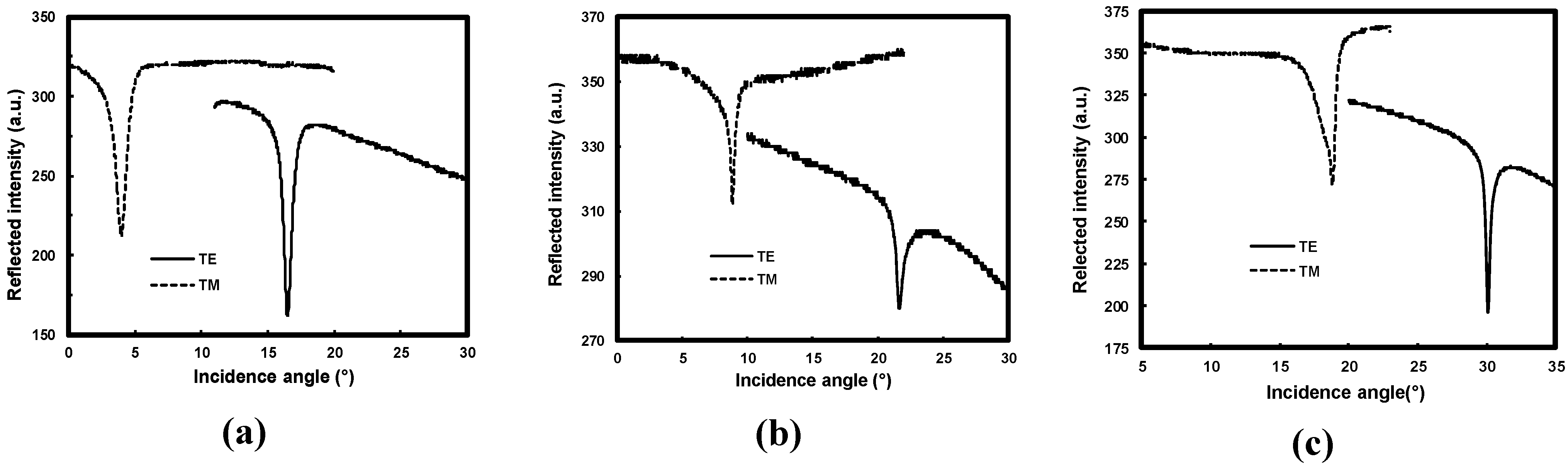
3.2.1. m-Lines Measurements

To investigate the waveguide optical properties of pure and Al-doped ZnO thin films, we used dark m-lines spectroscopy [47]. This technique is a useful method to determine the optogeometric parameters of waveguiding thin films, such as thickness and refractive index. It uses a prism coupling method to input the laser light into the optical film. In optical planar waveguides, light propagation can occur within a thin film of a transparent material when its refractive index is higher than that of surrounding layers and when the film has sufficient thickness to support at least one guided mode. In addition, the waveguiding properties of the film strongly depend on the microstructure of the material: surface roughness, porosity, and grain size which are connected to the fabrication process parameters such as spin speed, sol concentration, treatment temperature, and number of coating layers.
A well-characterized rutile prism is mounted onto a precise rotary stage (0.001°), which can be turned by a feedback-controlled DC motor. The mode profiles in both the TE and TM polarizations are obtained by measuring the reflected intensity of a (He-Ne) laser beam operating at a 632.8 nm wavelength, as a function of the incidence angle. The measurements were carried out on the film deposited on glass substrate. Figure 5 shows the typical TE and TM guided modes spectra of 7-layer, undoped, 1 at.% and 2 at.% Al-doped ZnO. The results show that our thin films support only the fundamental TE0 and TM0 modes.
Figure 5. Typical fundamental transverse electric (TE) and transverse magnetic (TM) guided mode spectra of 7-layer ZnO thin film (a) undoped, (b) 1 at.% Al-doped, (c) 2 at.% Al-doped.
Coatings 03 00126 g005
From the angular position of the reflectivity dips, we compute the effective mode indices. These last ones serve to calculate the refractive indices and the thickness of the film. These parameters are related to the effective mode indices by the following dispersion relationship [47]:
Coatings 03 00126 i002
where:
Coatings 03 00126 i003
For TE mode ρ = 0 and n = nTE and for the TM mode ρ = 1 and n = nTM, where Coatings 03 00126 i005 and Coatings 03 00126 i006 are the phase shift at air/film and film/substrate interfaces, d is the film thickness, λ is the wavelength of the light in vacuum, na and ns are, respectively, the air and substrate refractive indices, m the mode number and Nm the effective index of the mth mode. From Equation 2 we computed the refractive indices and thickness of the film from the measured effective mode indices. At least two modes are generally needed. Because our waveguides are single mode, we use the measured value of the effective indices and that of thickness measured by the SEM. The calculation is based on the least square method widely discussed by Kersten [53] and the results are reported in Table 2.
Table 2. Measured fundamental TE and TM effective indices, thickness and refractive indices of the undoped, 1 at.% Al and 2 at.% Al-doped 7-layer ZnO thin films.
SampleUndoped ZnO1 at.% Al-doped ZnO2 at.% Al-doped ZnO
Thickness (nm), d325320240
PolarizationTETMTETMTETM
Effective index, N01.75401.72531.73691.70661.64251.5937
Refractive index, n1.86991.88621.85451.86981.80231.8137
The results show that doping ZnO with aluminum result in a decrease of the refractive index for both TE and TM polarizations compared to undoped one. These results are in agreement with previous works reported by Xue et al. [37]. Indeed, the authors reported the effects of Al doping concentration on optical constants of AZO thin films by analysing the transmittance spectrum, which showed that the refractive index decreases with the increase of the Al doping concentration.
We also noted from the full width at half maximum (FWHM) of the modes spectra of Al-doped ZnO waveguides that the guided modes are better confined and will exhibit low propagation losses compared to undoped ones.

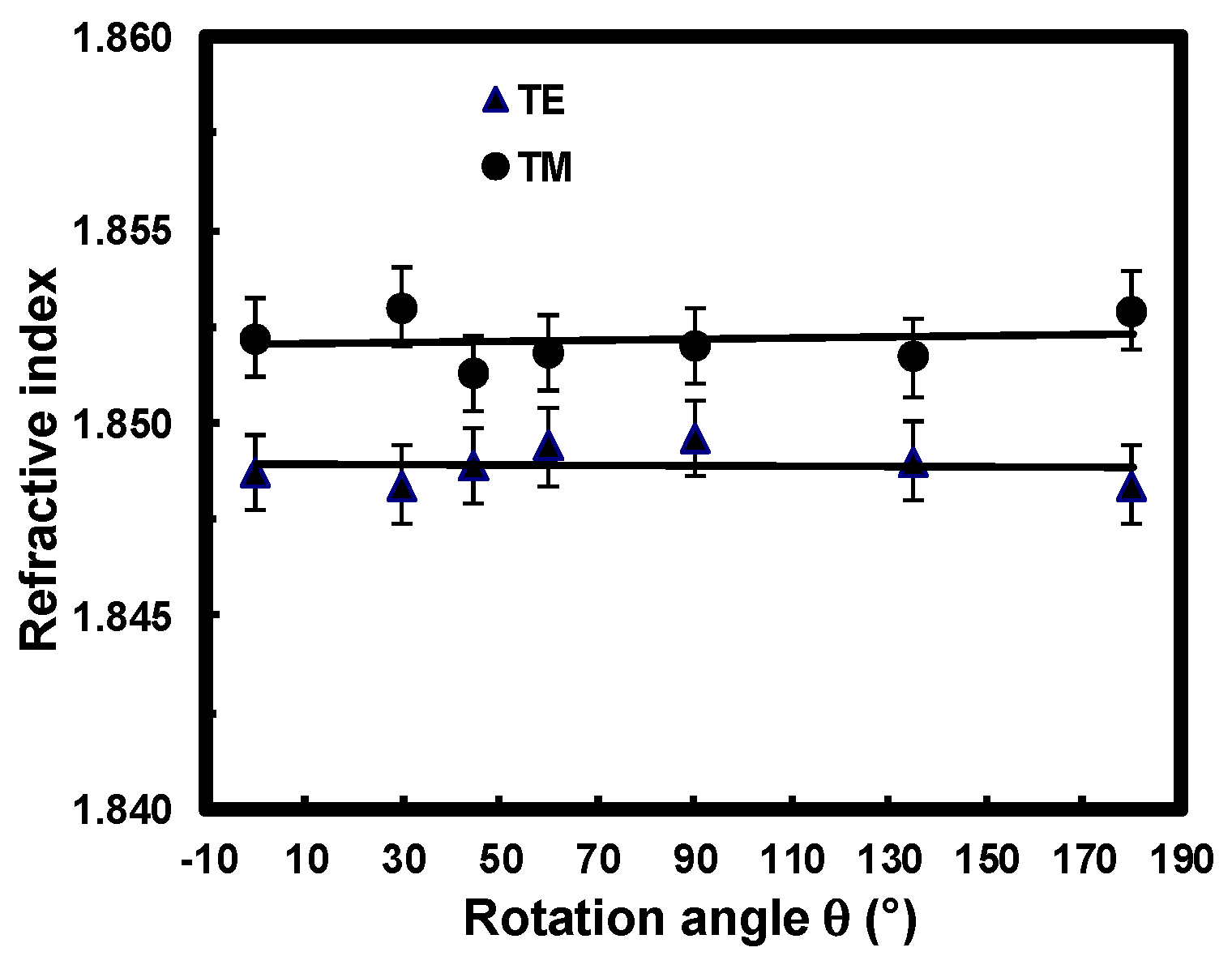
3.2.2. Optical Anisotropy Study

To study the orientation of the optical axis, and confirm the previous results, we turn our interest to the investigation of the optical anisotropy of the guiding region by using a modified m-lines setup. For this, a further degree of freedom is added to the prism coupler allowing us to rotate the sample beneath the prism around an axis perpendicular to its surface and laying parallel to the screw used for the coupling process. The sample is then rotated by an angle q related to a reference axis randomly fixed with respect to the length and the width of the sample. The waveguiding properties of the sample were studied for rotation angles ranging from θ = 0° to 180°. For each position, both TE and TM m-lines were recorded. Particular attention was paid to maintain the same coupling conditions (the coupling efficiency) to avoid any artefacts in the experiments. The TE and TM refractive indices are therefore determined as a function of the rotation angle. The results of the anisotropic measurements of ZnO thin film are reported in Figure 6. We noticed that TE and TM mode spectra are not influenced by the rotation of the sample. Their angular position and their general shape remain the same. Consequently, we deduced that the film is isotropic in the plane parallel to its surface with the optical axis perpendicular as previously indicated by the XRD patterns.
Figure 6. Measured refractive indices as a function of the rotation angle for TE and TM polarizations for the undoped 7-layer ZnO thin film.
Coatings 03 00126 g006

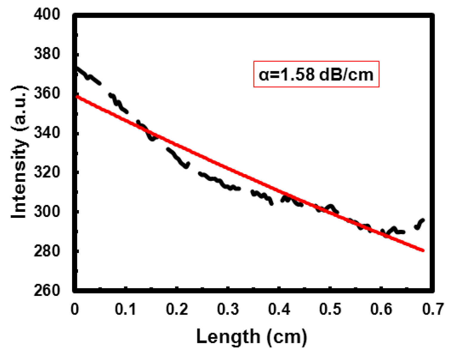
3.2.3. Optical Losses

The determination of optical attenuation in waveguides is of great interest for designing integrated optical devices. Practical use of such structures directly depends on the measurement of this parameter. Several techniques have been used for losses measurement among which the end-fire coupling [54], the prism coupling methods [55], and a new approach that uses a prism-in coupling method to feed the light into the waveguide and the end-fire coupling to measure the transmitted light [56].
For optical losses measurement, we have used the prism-in coupling and the moving fiber method (Metricon Model 2010) in which the exponential decay of light is measured by a fiber probe scanning down the length of the propagation streak. A least squares exponential fit is then made to the intensity as a function of distance patterns and the losses are calculated in dB/cm. The overall losses measured are the combined total of both scattering losses from particles or other scattering centers and surface roughness, and the inherent absorption of the waveguide material. The optical losses have been estimated around α = 1.6 dB.cm−1 using the following equation:
Coatings 03 00126 i004
where I0 is the initial light intensity, and IL is the light intensity at the considered position L, measured in centimeters. The result of the optical attenuation measured in a 7-layer undoped ZnO film is depicted in Figure 7.
Figure 7. Optical attenuation of the fundamental TE mode in undoped 7-layer ZnO thin film: surface scattering measurement (dotted line), with exponential fit (in red).
Coatings 03 00126 g007

4. Conclusions

In this work we reported the investigation of pure and Al-doped ZnO thin films prepared by sol-gel process for optical waveguiding applications.
The prepared samples display a very strong Texture Coefficient for the (002) direction. SEM and AFM characterizations have been focused on morphology, crystalline sizes, and roughness (RMS), the latter being known to be strongly correlated to the optical losses.
The optical properties determined by m-lines spectroscopy are promising for further waveguiding applications. All the films are displaying well-guided modes meaning that the coupling and confinement of the light in the film is efficient. We have shown that doping ZnO with aluminum leads to a decrease in the refractive index for both TE and TM polarizations, but in the meantime the roughness of the layer is decreased and no deterioration of the waveguiding properties was observed.
The optical anisotropy study has confirmed the results obtained by XRD characterization, indicating that the diffraction patterns are typical of the wurtzite hexagonal structure with preferably a perpendicular c-axis orientation to the surface.
The optical losses were estimated to be around 1.6 dB/cm using the moving fiber method. Therefore, the sol-gel method was proved to be well-adapted to the elaboration of thin films for photonic applications.

Acknowledgments

ANR (Agence Nationale de la Recherche) and CGI (Commissariat à l’Investissement d’Avenir) are gratefully acknowledged for their financial support of this work through Labex SEAM (Science and Engineering for Advanced Materials and devices).

References

  1. Ellmer, K.; Klein, A. ZnO and Its Applications. In Transparent Conductive Zinc Oxide—Basics and Applications in Thin Film Solar Cells; Springer Series in Materials Science; Ellmer, K., Klein, A., Rech, B., Eds.; Springer-Verlag: Berlin Heidelberg, Germany, 2008; Volume 104, pp. 1–33. [Google Scholar]
  2. Bundesmann, C.; Schmidt-Grund, R.; Schubert, M. Optical Properties of ZnO and Related Compounds. In Transparent Conductive Zinc Oxide—Basics and Applications in Thin Film Solar Cells (Springer Series in Materials Science); Ellmer, K., Klein, A., Rech, B., Eds.; Springer-Verlag: Berlin Heidelberg, Germany, 2008; Volume 104, pp. 79–124. [Google Scholar]
  3. Chen, J.L.; Chen, D.; Chen, Z.H. Optimization of the process for preparing Al-doped ZnO thin films by sol-gel method. Sci. China Ser. E Tech. Sci. 2009, 52, 88–94. [Google Scholar] [CrossRef]
  4. Tseng, Y.K.; Gao, G.J.; Chien, S.C. Synthesis of c-axis preferred orientation ZnO:Al transparent conductive thin films using a novel solvent method. Thin Solid Films 2010, 518, 6259–6263. [Google Scholar] [CrossRef]
  5. Lupan, O.; Chow, L.; Shishiyanu, S.; Monaico, E.; Shishiyanu, T.; Şontea, V.; Roldan Cuenya, B.; Naitabdi, A.; Park, S.; Schulte, A. Nanostructured zinc oxide films synthesized by successive chemical solution deposition for gas sensor applications. Mater. Res. Bull. 2009, 44, 63–69. [Google Scholar] [CrossRef]
  6. Lupan, O.; Shishiyanu, S.; Ursaki, V.; Khallaf, H.; Chow, L.; Shishiyanu, T.; Sontea, V.; Monaico, E.; Railean, S. Synthesis of nanostructured Al-doped zinc oxide films on Si for solar cells applications. Sol. Energy. Mater. Sol. Cells 2009, 93, 1417–1422. [Google Scholar] [CrossRef]
  7. Von Wenckstern, H.; Schmidt, H.; Brandt, M.; Lajn, A.; Pickenhain, R.; Lorenz, M.; Grundmann, M.; Hofmann, D.M.; Polity, A.; Meyer, B.K.; et al. Anionic and cationic substitution in ZnO. Prog. Solid State Chem. 2009, 37, 153–172. [Google Scholar] [CrossRef]
  8. Özgür, Ü.; Alivov Ya, I.; Liu, C.; Teke, A.; Reshchikov, M.A.; Doğan, S.; Avrutin, V.; Cho, S.J.; Morkoç, H. A comprehensive review of ZnO materials and devices. J. Appl. Phys. 2005, 98, 041301:1–041301:103. [Google Scholar]
  9. Schmidt-Mende, L.; MacManus-Driscoll, J.L. ZnO-nanostructures, defects, and devices. Mater. Today 2007, 10, 40–48. [Google Scholar] [CrossRef]
  10. Leprince-Wang, Y.; Bouchaib, S.; Brouri, T.; Capo-chichi, M.; Laurent, K.; Leopoldes, J.; Tusseau-Nenez, S.; Lei, L.; Chen, Y. Fabrication of ZnO micro- and nano-structures by electrodeposition using nanoporous and lithography defined templates. Mater. Sci. Eng. B 2010, 170, 107–112. [Google Scholar] [CrossRef]
  11. Vayssieres, L. Growth of arrayed nanorods and nanowires of ZnO from aqueous solutions. Adv. Mater. 2003, 15, 464–466. [Google Scholar] [CrossRef]
  12. Chandramohan, R.; Vijayan, T.A.; Arumugam, S.; Ramalingam, H.B.; Dhanasekaran, V.; Sundaram, K.; Mahalingam, T. Effect of heat treatment on microstructural and optical properties of CBD grown Al-doped ZnO thin films. Mater. Sci. Eng. B 2011, 176, 152–156. [Google Scholar] [CrossRef]
  13. Barankin, M.D.; Gonzalez, E., II; Ladwig, A.M.; Hicks, R.F. Plasma-enhanced chemical vapor deposition of zinc oxide at atmospheric pressure and low temperature. Sol. Energy. Mater. Sol. Cells 2007, 91, 924–930. [Google Scholar]
  14. Dai, L.P.; Deng, H.; Zang, J.D.; Mao, F.Y.; Chen, J.J.; Wei, M. The effect of annealing temperature on the properties of ZnO films with preferential nonpolar plane orientation by SSCVD. J. Mater. Sci. 2008, 43, 312–315. [Google Scholar]
  15. Triboulet, R.; Perrière, J. Epitaxial growth of ZnO films. Prog. Cryst. Growth Charact. Mater. 2003, 47, 65–138. [Google Scholar]
  16. Szyszka, B. Magnetron Sputtering of ZnO Films. In Transparent Conductive Zinc Oxide—Basics and Applications in Thin Film Solar Cells; Springer Series in Materials Science; Ellmer, K., Klein, A., Rech, B., Eds.; Springer-Verlag: Berlin Heidelberg, Germany, 2008; Volume 104, pp. 187–233. [Google Scholar]
  17. Hüpkes, J.; Müller, J.; Rech, B. Texture Etched ZnO:Al for Silicon Thin Film Solar Cells. In Transparent Conductive Zinc Oxide—Basics and Applications in Thin Film Solar Cells; Springer Series in Materials Science; Ellmer, K., Klein, A., Rech, B., Eds.; Springer-Verlag: Berlin Heidelberg, Germany, 2008; Volume 104, pp. 359–413. [Google Scholar]
  18. Sekar, A.; Kim, S.H.; Umar, A.; Hahn, Y.B. Catalyst-free synthesis of ZnO nanowires on Si by oxidation of Zn powders. J. Cryst. Growth 2005, 277, 471–478. [Google Scholar] [CrossRef]
  19. Ibanga, E.J.; le Luyer, C.; Mugnier, J. Zinc oxide waveguide produced by thermal oxidation of chemical bath deposited zinc sulphide thin films. Mater. Chem. Phys. 2003, 80, 490–495. [Google Scholar] [CrossRef]
  20. Caglar, M.; Ilican, S.; Caglar, Y.; Yakuphanoglu, F. The effects of Al doping on the optical constants of ZnO thin films prepared by spray pyrolysis method. J. Mater. Sci. Mater. Electron. 2008, 19, 704–708. [Google Scholar] [CrossRef]
  21. Yen, C.Y.; Jian, S.R.; Chen, G.J.; Lin, C.M.; Lee, H.Y.; Ke, W.C.; Liao, Y.Y.; Yang, P.F.; Wang, C.T.; Lai, Y.S.; et al. Influence of annealing temperature on the structural, optical and mechanical properties of ALD-derived ZnO thin films. Appl. Surf. Sci. 2011, 257, 7900–7905. [Google Scholar] [CrossRef]
  22. Ghodsi, F.E.; Absalan, H. Comparative study of ZnO thin films prepared by different sol-gel route. Acta. Phys. Pol. A 2010, 118, 659–664. [Google Scholar]
  23. Znaidi, L. Sol-gel-deposited ZnO thin films: A review. Mater. Sci. Eng. B 2010, 174, 18–30. [Google Scholar] [CrossRef]
  24. Ohyama, M.; Kozuka, H.; Yoko, T.; Sakka, S. Preparation of ZnO films with preferential orientation by sol-gel method. J. Ceram. Soc. Jpn. 1996, 104, 296–300. [Google Scholar] [CrossRef]
  25. Ohyama, M.; Kozuka, H.; Yoko, T. Sol-Gel preparation of ZnO films with extremely preferred orientation along (002) plane from zinc acetate solution. Thin Solid Films 1997, 306, 78–85. [Google Scholar] [CrossRef]
  26. Znaidi, L.; Soler Illia, G.J.A.A.; Ben Yahia, S.; Sanchez, C.; Kanaev, A. Oriented ZnO thin films synthesis by sol-gel process for laser application. Thin Solid Films 2003, 428, 257–262. [Google Scholar] [CrossRef]
  27. Znaidi, L.; Soler Illia, G.J.A.A.; Le Guennic, R.; Sanchez, C.; Kanaev, A. Elaboration of ZnO thin films with preferential orientation by a soft chemistry route. J. Sol-Gel Sci. 2003, 26, 817–821. [Google Scholar] [CrossRef]
  28. Ben Yahia, S.; Znaidi, L.; Kanaev, A.; Petitet, J.P. Raman study of oriented ZnO thin films deposited by sol-gel method. Spectrochim. Acta Part. A 2008, 71, 1234–1238. [Google Scholar] [CrossRef]
  29. Xue, S.W.; Zu, X.T.; Zhou, W.L.; Deng, H.X.; Xiang, X.; Zhang, L.; Deng, H. Effects of post-thermal annealing on the optical constants of ZnO thin film. J. Alloys Compd. 2008, 448, 21–26. [Google Scholar] [CrossRef]
  30. Serbetçi, Z.; El-Nasser, H.M.; Yakuphanoglu, F. Photoluminescence and refractive index dispersion properties of ZnO nanofibers grown by sol-gel method. Spectrochim. Acta Part. A 2012, 86, 405–409. [Google Scholar] [CrossRef]
  31. Tang, W.; Cameron, D.C. Aluminum-doped zinc oxide transparent conductors deposited by the sol-gel process. Thin Solid Films 1994, 238, 83–87. [Google Scholar] [CrossRef]
  32. Ohyama, M. Sol-Gel preparation of transparent and conductive aluminum-doped zinc oxide films with highly preferential crystal orientation. J. Am. Ceram. Soc. 1998, 81, 1622–1632. [Google Scholar] [CrossRef]
  33. Schuler, T.; Aegerter, M.A. Optical, electrical and structural properties of sol-gel ZnO:Al coatings. Thin Solid Films 1999, 351, 125–131. [Google Scholar] [CrossRef]
  34. Bandyopadhyay, S.; Paul, G.K.; Roy, R.; Sen, S.K.; Sen, S. Study of structural and electrical properties of grain-boundary modified ZnO films prepared by sol-gel technique. Mater. Chem. Phys. 2002, 74, 83–91. [Google Scholar] [CrossRef]
  35. Cheong, K.Y.; Norani Muti, M.; Sutapa, R.R. Physical Investigation on ZnO:Al Thin films derived from non-alkoxide zinc acetate via sol-gel dip coating technique. J. Mater. Sci. Technol. 2003, 11, 78–83. [Google Scholar]
  36. Lee, J.H.; Park, B.O. Transparent conducting ZnO:Al, In and Sn thin films deposited by the sol-gel method. Thin Solid Films 2003, 426, 94–99. [Google Scholar] [CrossRef]
  37. Xue, S.W.; Zu, X.T.; Zheng, W.G.; Deng, H.X.; Xiang, X. Effects of Al doping concentration on optical parameters of ZnO:Al thin films by sol-gel technique. Physica B 2006, 381, 209–213. [Google Scholar] [CrossRef]
  38. Lai, C.M.; Lin, K.M.; Rosmaidah, S. Effect of annealing temperature on the quality of Al-doped ZnO thin films prepared by sol-gel method. J. Sol.-Gel Sci. Technol. 2011. [Google Scholar] [CrossRef]
  39. Khan, F.; Singh, V.S.N.; Husain, M.; Singh, P.K. Sol-gel derived hydrogen annealed ZnO:Al films for silicon solar cell application. Sol. Energy. Mater. Sol. Cells 2012, 100, 57–60. [Google Scholar] [CrossRef]
  40. Altamirano-Juárez, D.C.; Torres-Delgado, G.; Jiménez-Sandoval, S.; Jiménez-Sandoval, O.; Castanedo-Pérez, R. Low-resistivity ZnO:F:Al transparent thin films. Sol. Energy. Mater. Sol. Cells 2004, 82, 35–43. [Google Scholar]
  41. Lv, J.; Huang, K.; Chen, X.; Zhu, J.; Cao, C.; Song, X.; Sun, Z. Optical constants of Na-doped ZnO thin films by sol-gel method. Opt. Commun. 2011, 284, 2905–2908. [Google Scholar]
  42. Caglar, M.; Yakuphanoglu, F. Structural and optical properties of copper doped ZnO films derived by sol-gel. Appl. Surf. Sci. 2012, 258, 3039–3044. [Google Scholar]
  43. Tsay, C.Y.; Cheng, H.C.; Tung, Y.T.; Tuan, W.H.; Lin, C.K. Effect of Sn-doped on microstructural and optical properties of ZnO thin films deposited by sol-gel method. Thin Solid Films 2008, 517, 1032–1036. [Google Scholar] [CrossRef]
  44. Shelke, V.; Sonawane, B.K.; Bhole, M.P.; Patil, D.S. Electrical and optical properties of transparent conducting tin doped ZnO thin films. J. Mater. Sci. 2012, 23, 451–456. [Google Scholar]
  45. Liu, C.; Yun, F.; Morkoç, H. Ferromagnetism of ZnO and GaN: A review. J. Mater. Sci. Mater. Electron. 2005, 16, 555–597. [Google Scholar]
  46. Mueller, J.; Mahnke, M.; Schoer, G.; Wiechmann, S. Inorganic Materials Integrated Optics. AIP Conf. Proc. 2004, 709, 268–289. [Google Scholar] [CrossRef]
  47. Tien, P.K.; Ulrich, R. Theory of prism-film coupler and thin-film light guides. J. Opt. Soc. Am. 1970, 60, 1325–1337. [Google Scholar] [CrossRef]
  48. Chen, J.; Chen, D.; He, J.; Zhang, S.; Chen, Z. The microstructure, optical, and electrical properties of sol-gel-derived Sc-doped and Al-Sc co-doped ZnO thin films. Appl. Surf. Sci. 2009, 255, 9413–9419. [Google Scholar] [CrossRef]
  49. Fityk. Available online: http://fityk.nieto.pl/ (accessed on 1 June 2013).
  50. Barret, C.S.; Massalski, T.B. Structure of Metals: Crystallographic Methods, Principles and Data; Pergamon Press: Oxford, UK, 1980; p. 204. [Google Scholar]
  51. Williamson, G.K.; Hall, W.H. X-ray line broadening from filed aluminium and wolfram. Acta Metall. 1953, 1, 22–31. [Google Scholar] [CrossRef]
  52. Burton, A.W.; Ong, K.; Rea, T.; Chan, I.Y. On the estimation of average crystallite size of zeolites from the Scherrer equation: A critical evaluation of its application to zeolites with one-dimensional pore systems. Microporous. Mesoporous. Mater. 2009, 117, 75–90. [Google Scholar] [CrossRef]
  53. Kersten, R.Th. Numerical solution of the mode-equation of planar dielectric waveguides to determine their refractive index and thickness by means of a prism-film coupler. Opt. Commun. 1973, 9, 427–431. [Google Scholar] [CrossRef]
  54. Strohkendl, F.P.; Fluck, D.; Günter, P.; Irmscher, R.; Buchal, Ch. Nonleaky optical waveguides in KNbO3 by ultralow dose MeV He ion implantation. Appl. Phys. Lett. 1991, 59, 3354–3356. [Google Scholar]
  55. Weber, H.P.; Dunn, F.A.; Leibolt, W.N. Loss measurements in thin-film optical waveguides. Appl. Opt. 1973, 12, 755–757. [Google Scholar] [CrossRef]
  56. Boudrioua, A.; Loulergue, J.C. New approach for loss measurements in optical planar waveguides. Opt. Commun. 1997, 137, 37–40. [Google Scholar] [CrossRef]

