
Thickness Measurement Methods for Physical Vapor Deposited Aluminum Coatings in Packaging Applications: A Review


Abstract
:1. Introduction
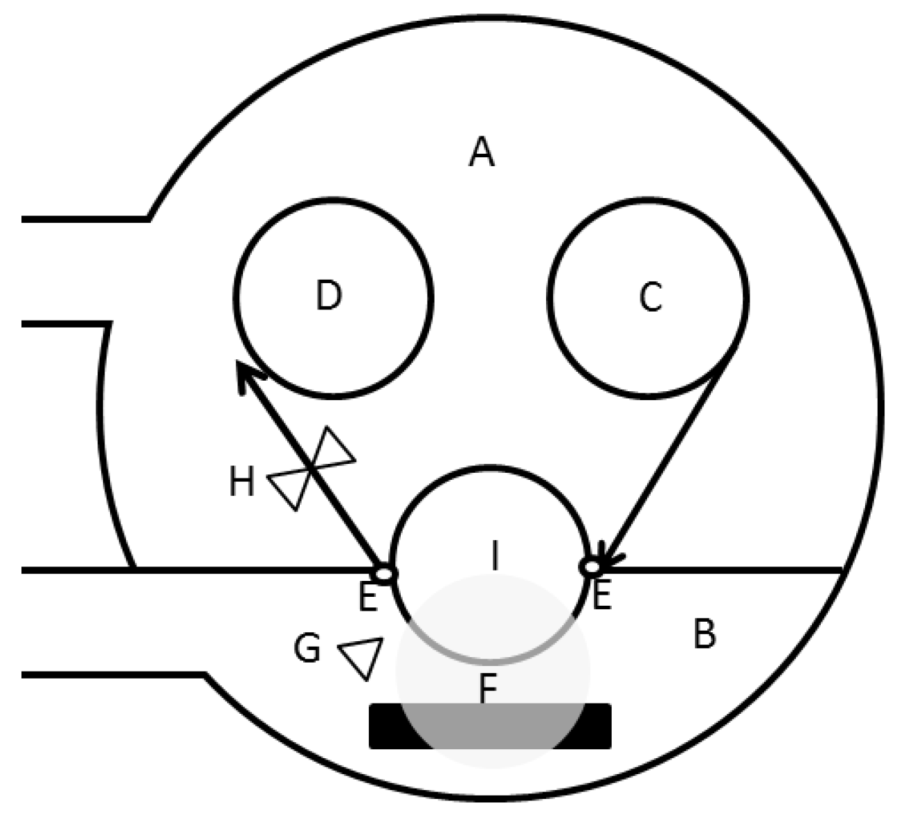
1.1. Deposition Techniques in Packaging Applications
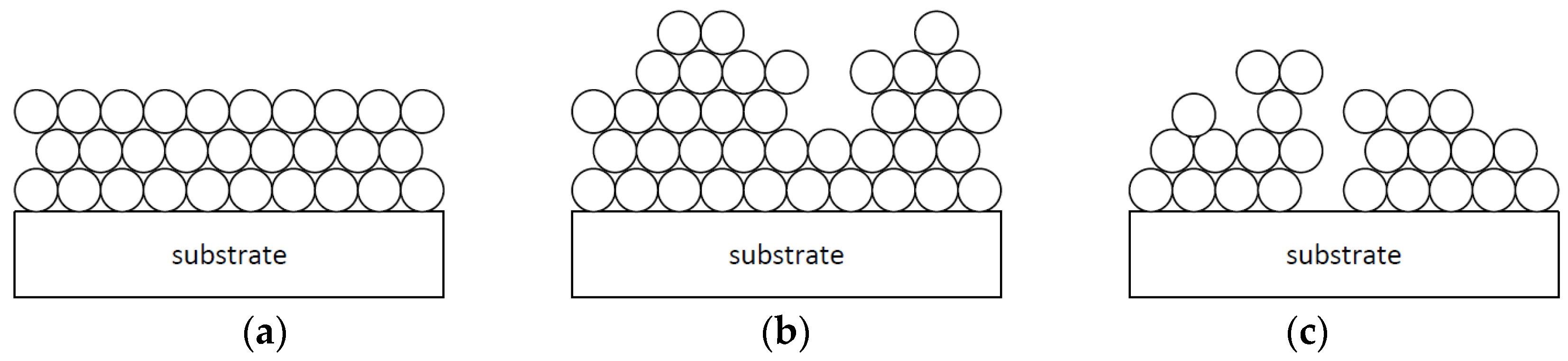
1.2. Application of Aluminum via Vacuum Evaporation and Layer Growth
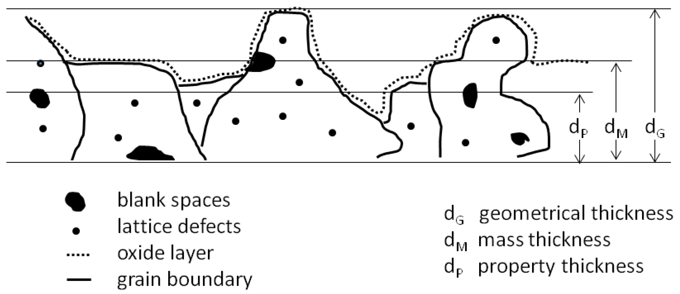
1.3. Pores and Defects
1.4. Formation of Aluminum Oxide
1.5. Permeation through Organic Substrates and Inorganic Coatings
1.6. Importance of Coating Thickness for Barrier Properties
2. Characterization Techniques
2.1. Mass Thickness
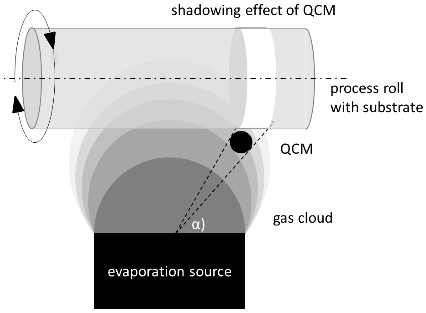
2.1.1. QCM
QCM: Theory
QCM: Method
QCM: Practical Aspects and Analyses
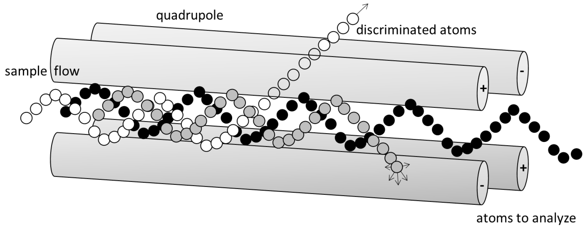
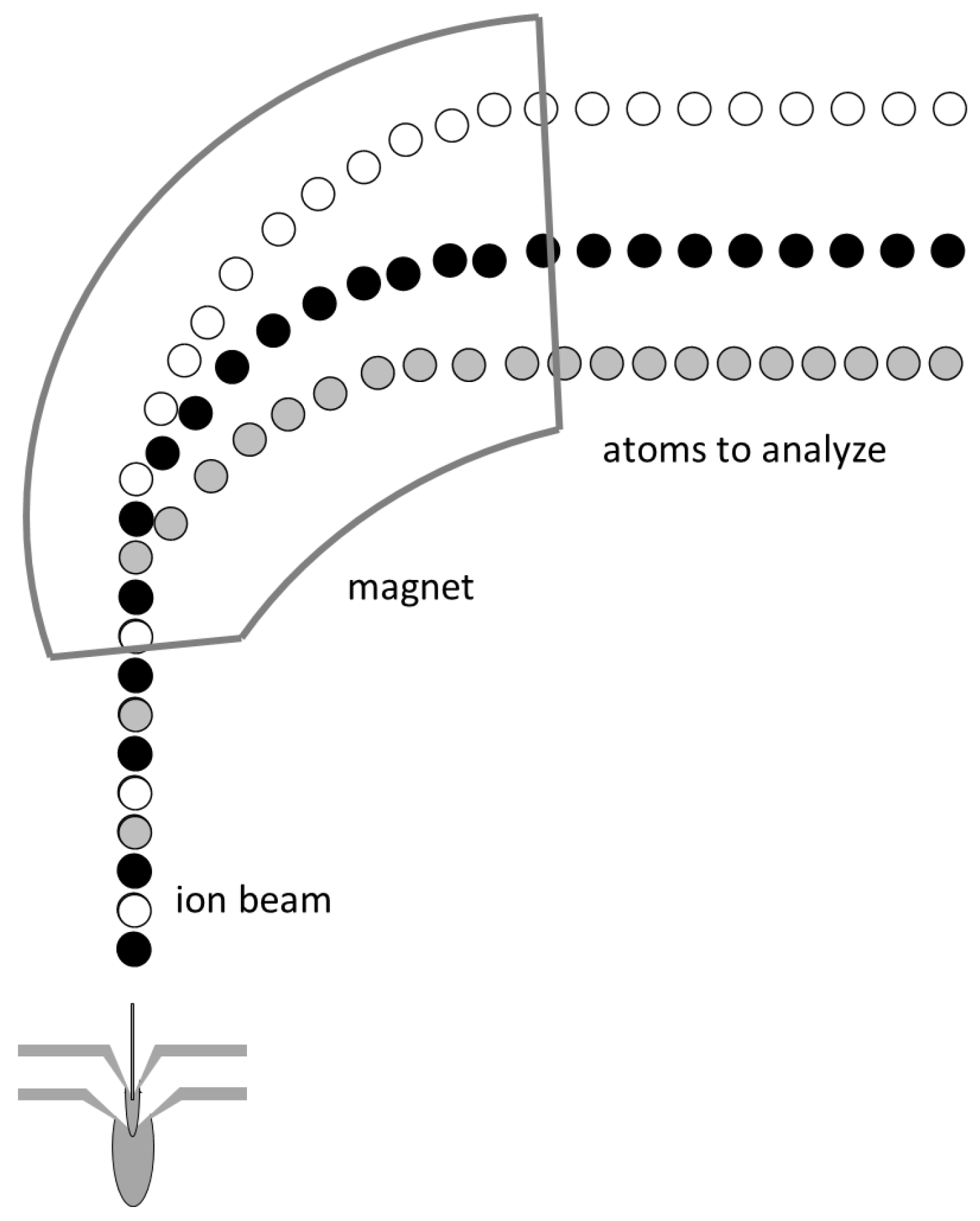
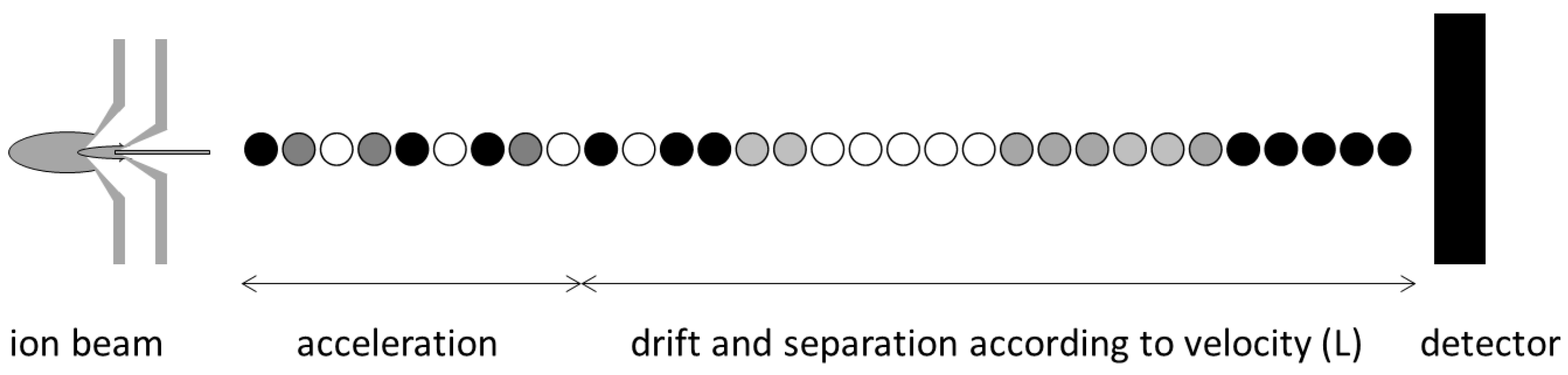
2.1.2. ICP-MS
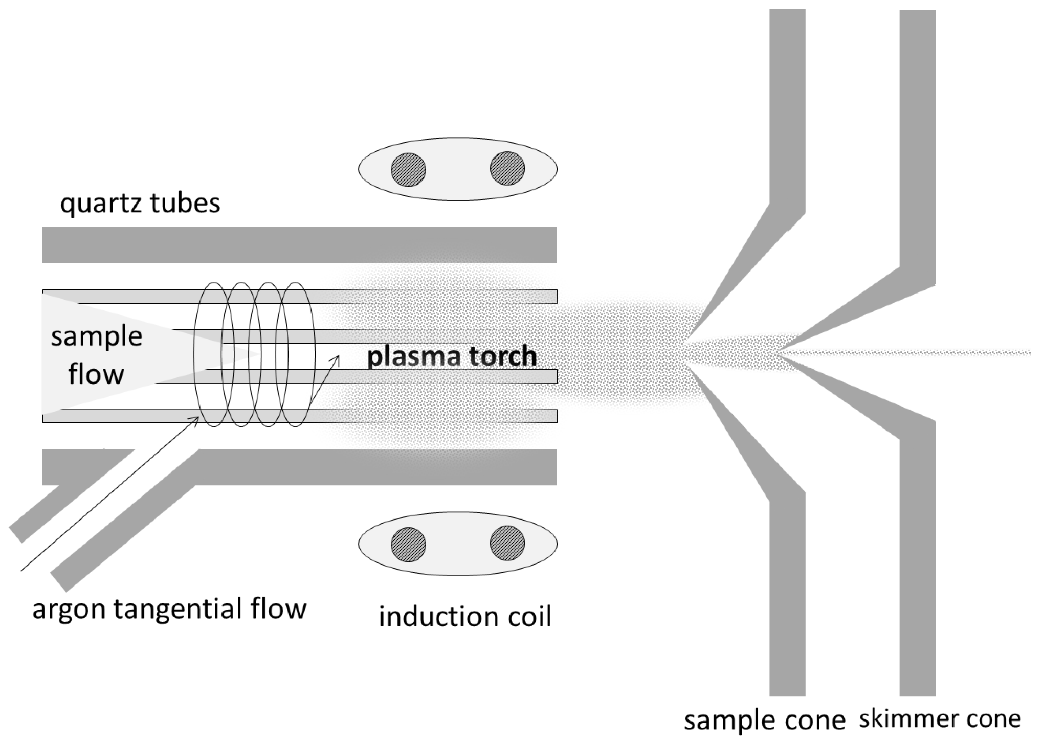
ICP-MS: Theory
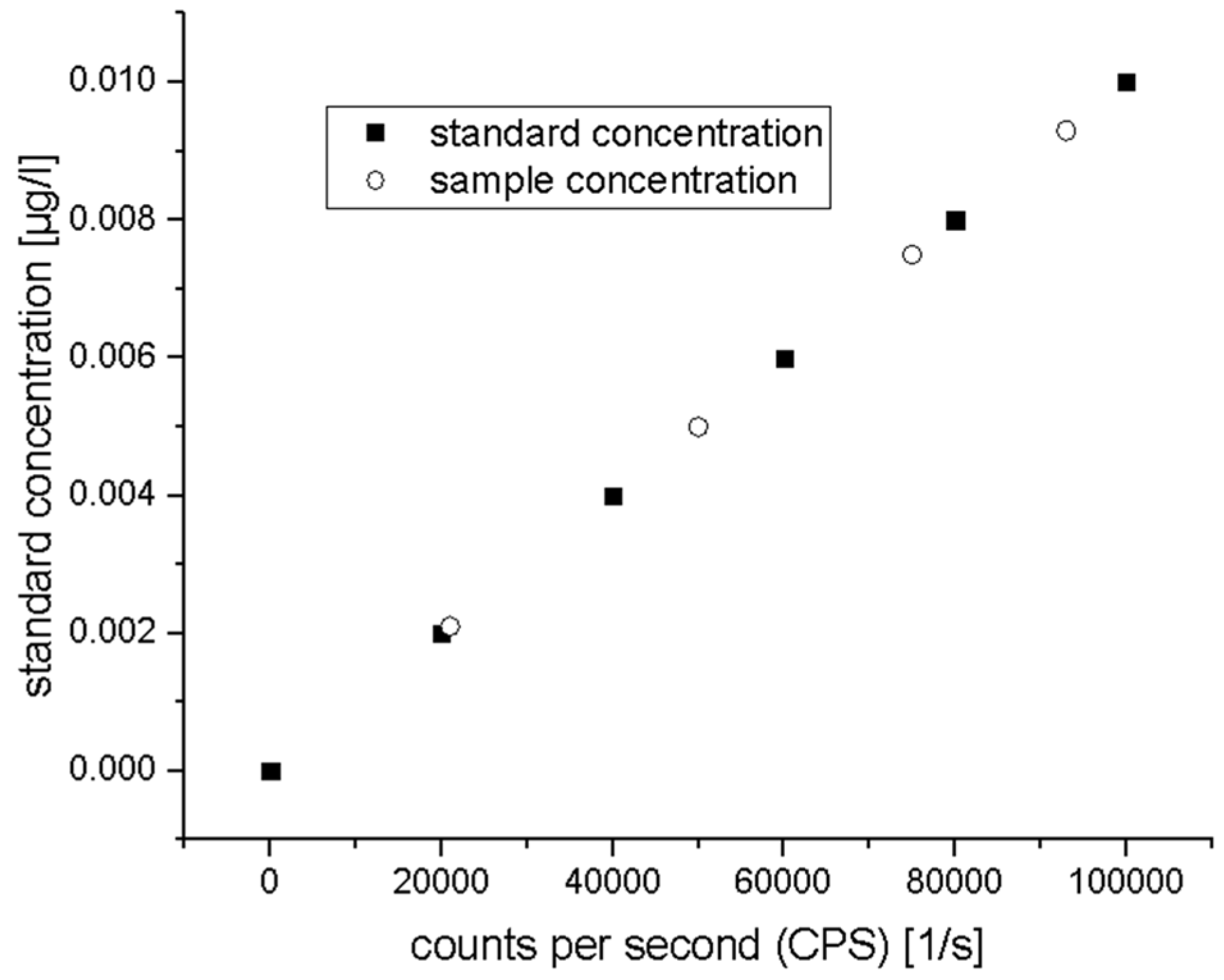
ICP-MS: Method
- Complete dissolution;
- Highly pure reagents;
- No chemical interaction between equipment and reagents;
- No loss of analyte.
ICP-MS: Practical Aspects and Analyses
2.2. Geometrical Thickness: AFM
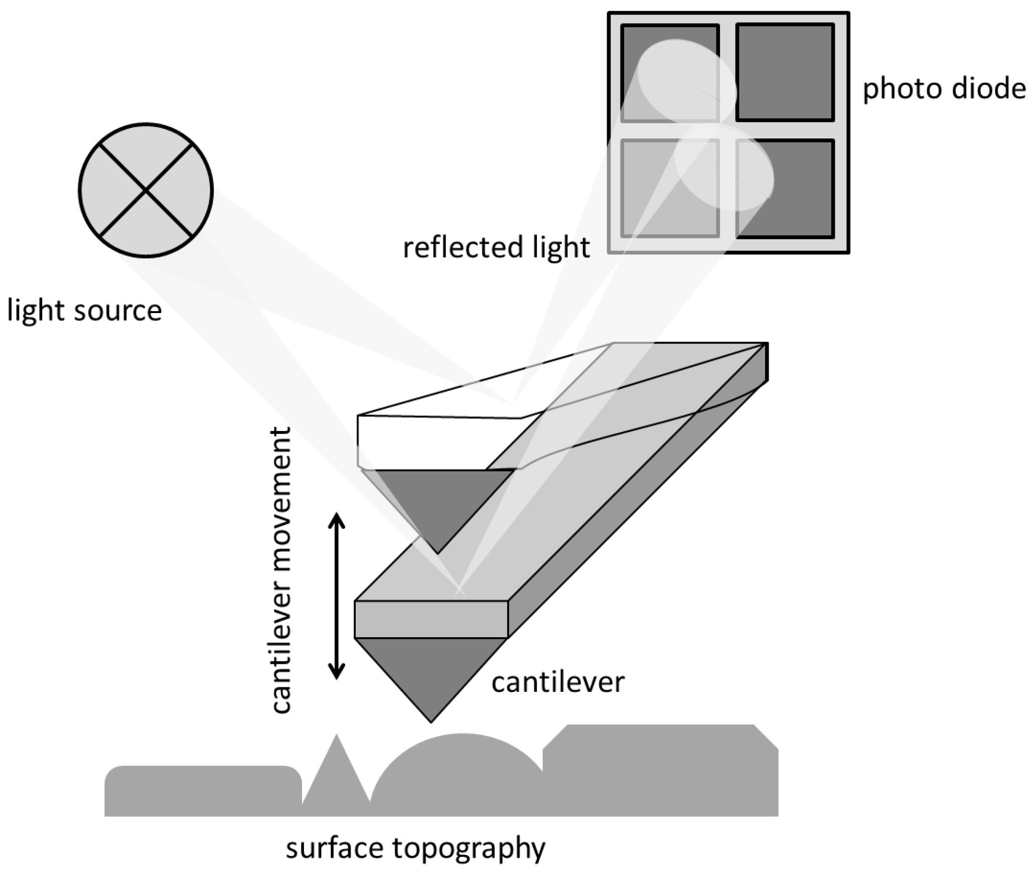
2.2.1. AFM
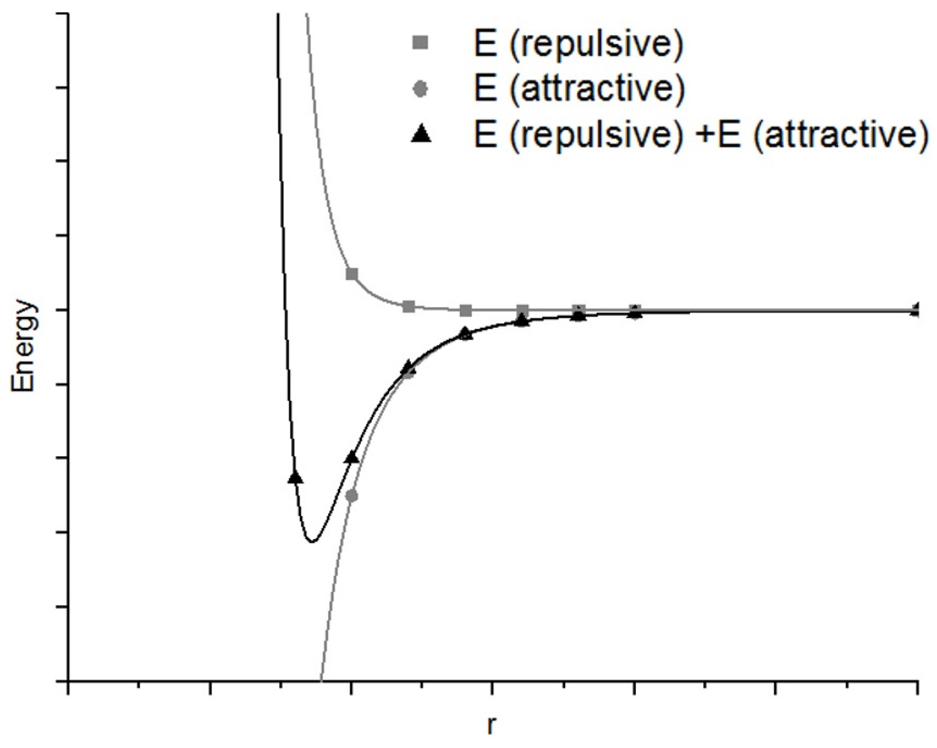
AFM: Theory
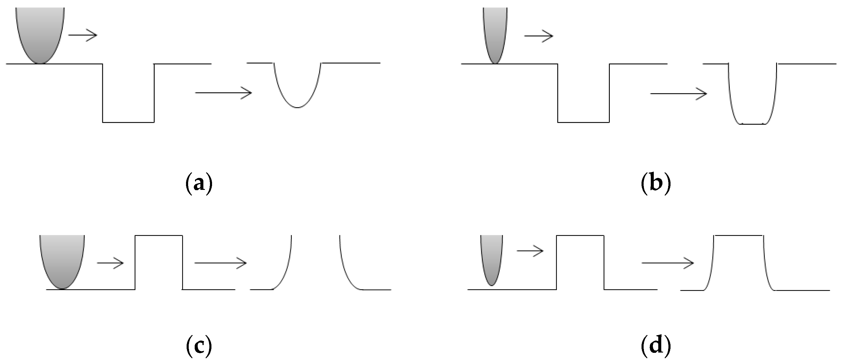
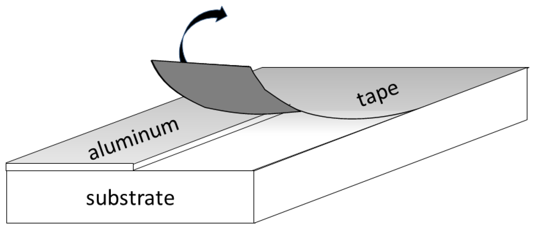
AFM: Method
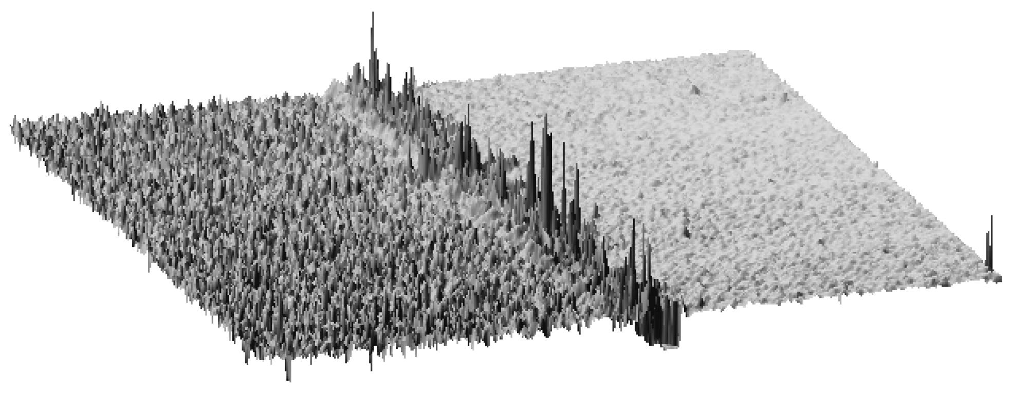
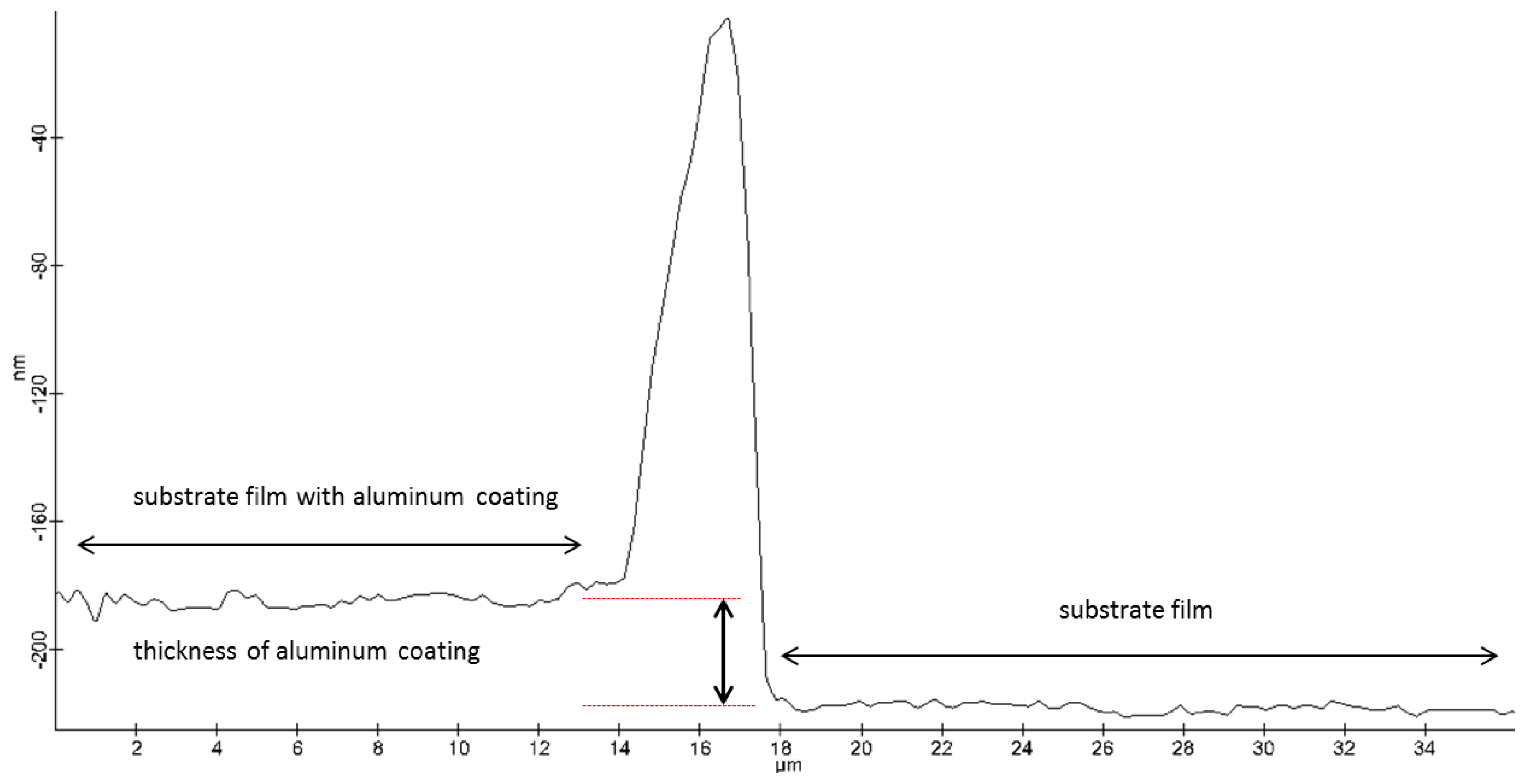
AFM: Practical Aspects and Analyses
2.3. Property Thickness
2.3.1. Optical Density
Optical Density: Theory
Optical Density: Method
Optical Density: Practical Aspects and Analyses
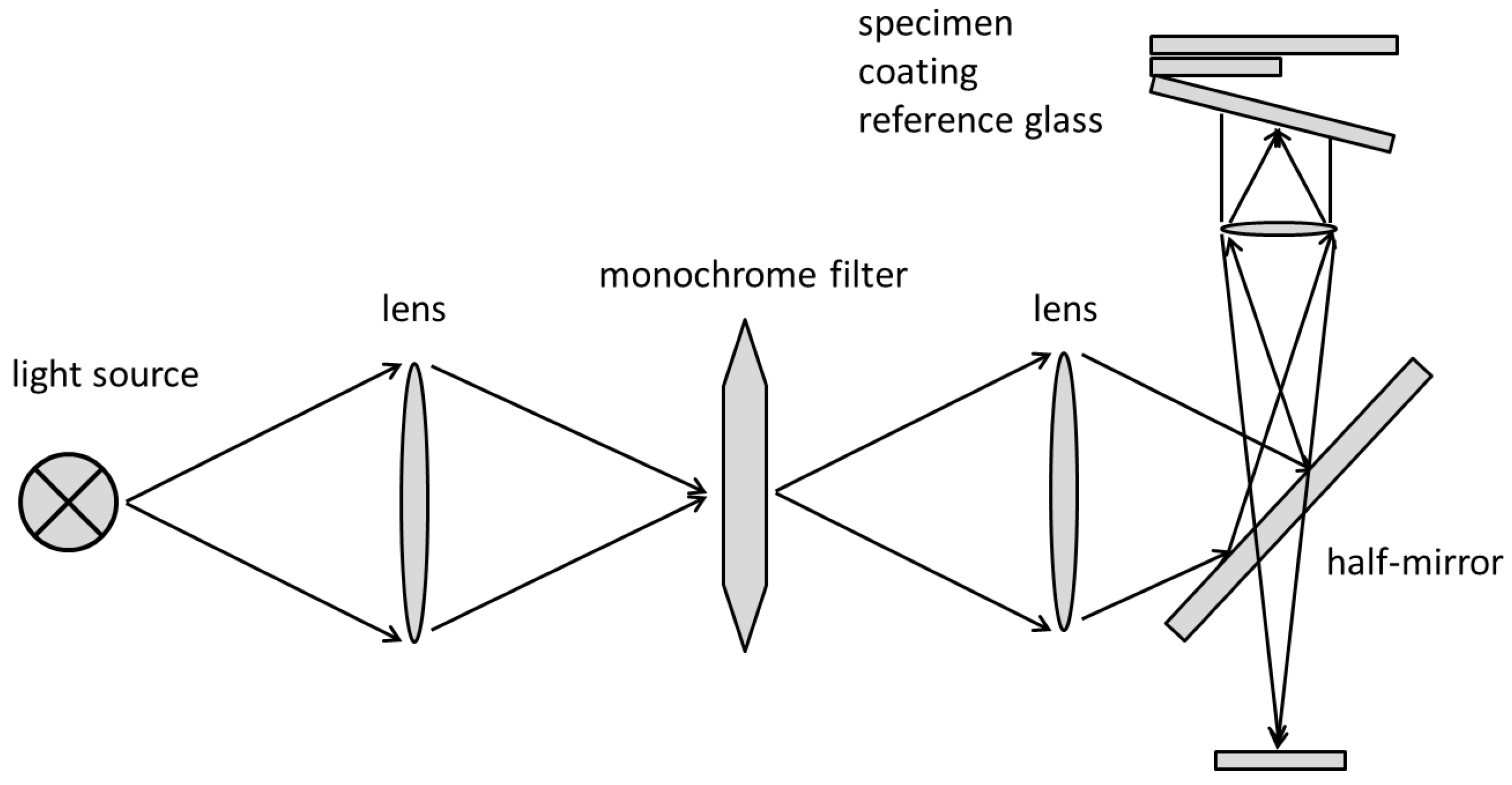
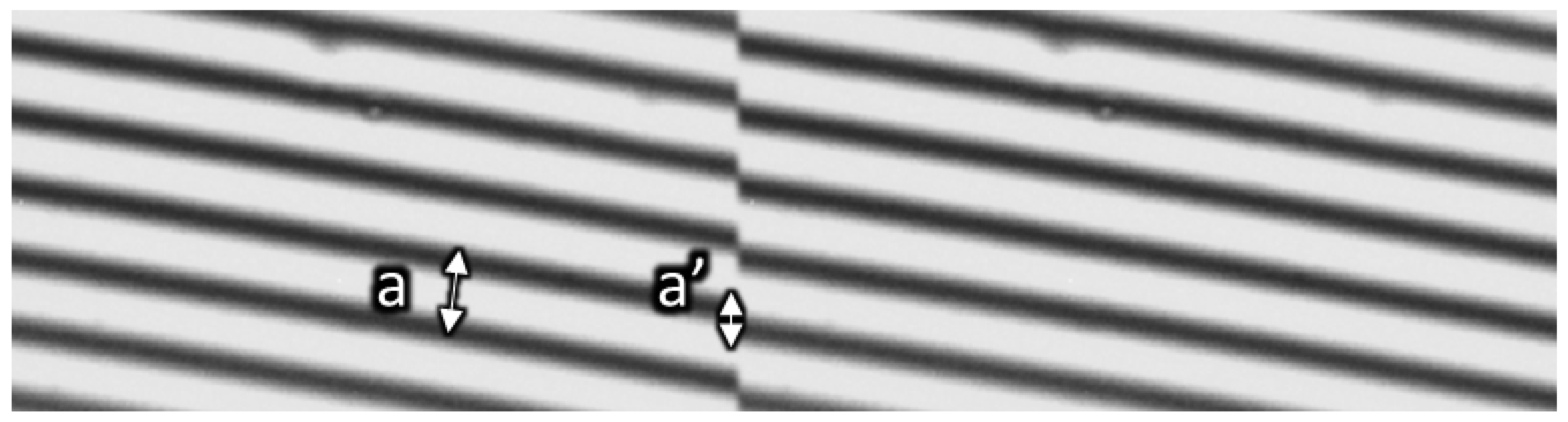
2.3.2. Interference (Tolansky Method)
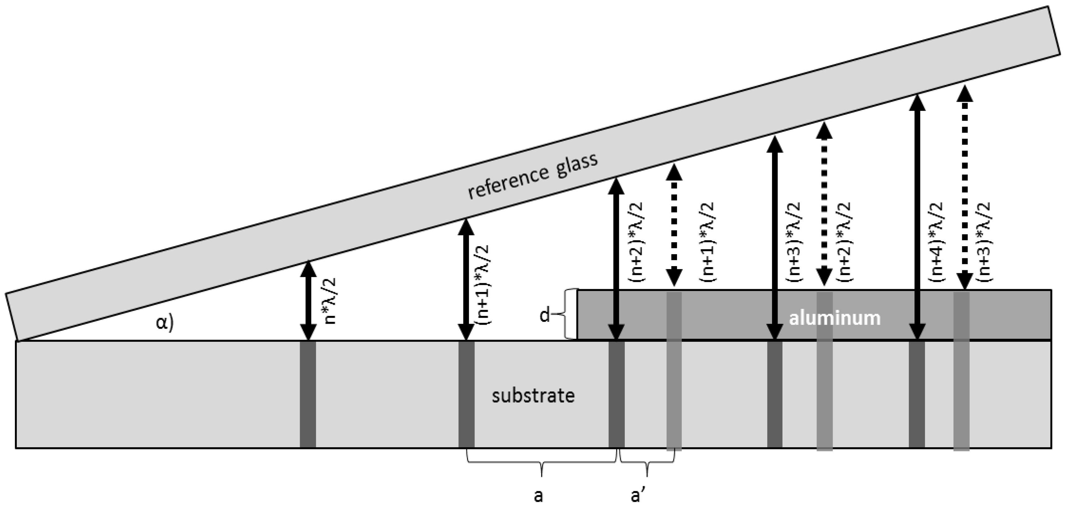
Interference (Tolansky Method): Theory
Interference (Tolansky Method): Method
Interference (Tolansky Method): Practical Aspects and Analyses
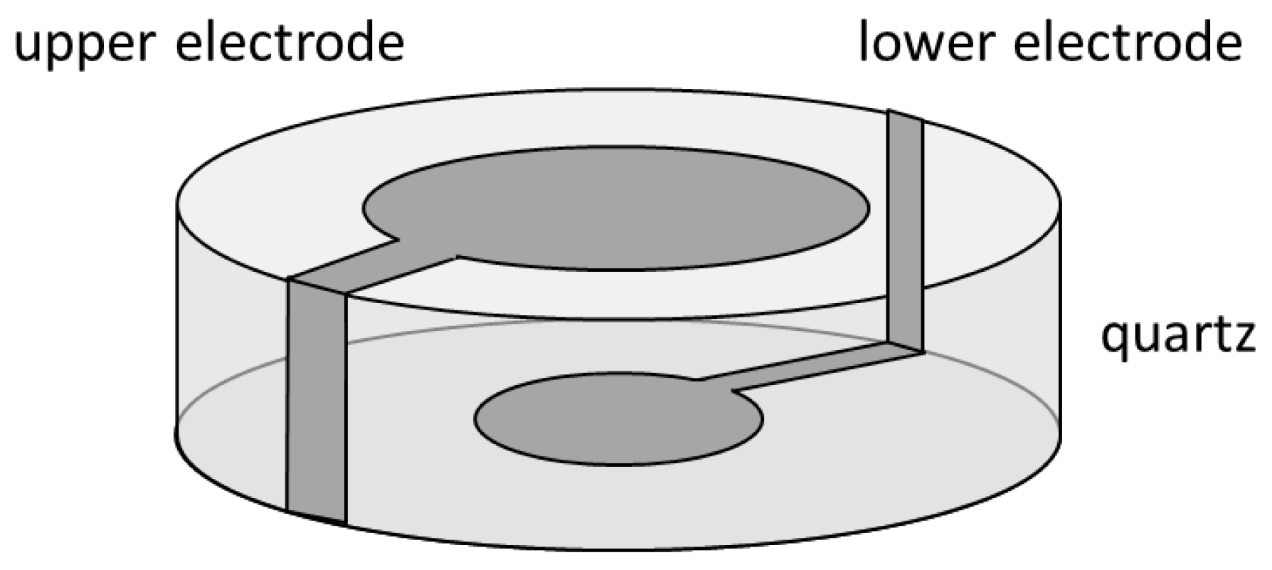
2.3.3. Electrical Surface Resistance
Electrical Surface Resistance: Theory
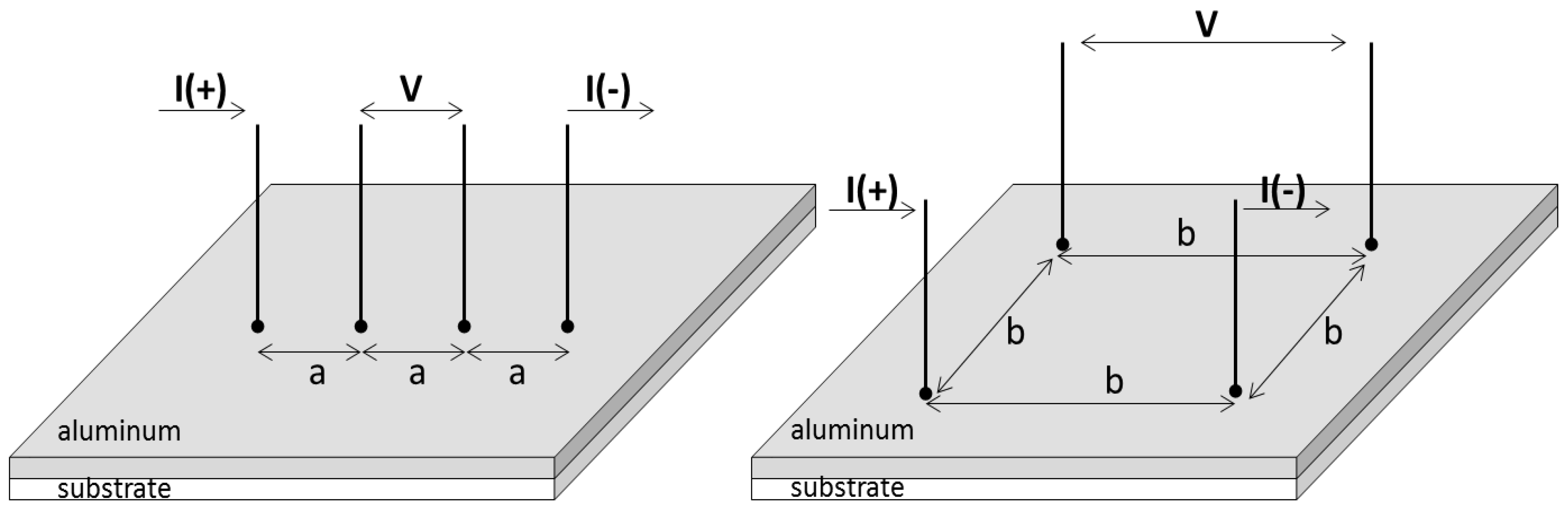
Electrical Surface Resistance: Method
Electrical Surface Resistance: Practical Aspects and Analyses
2.3.4. Eddy Current Measurement
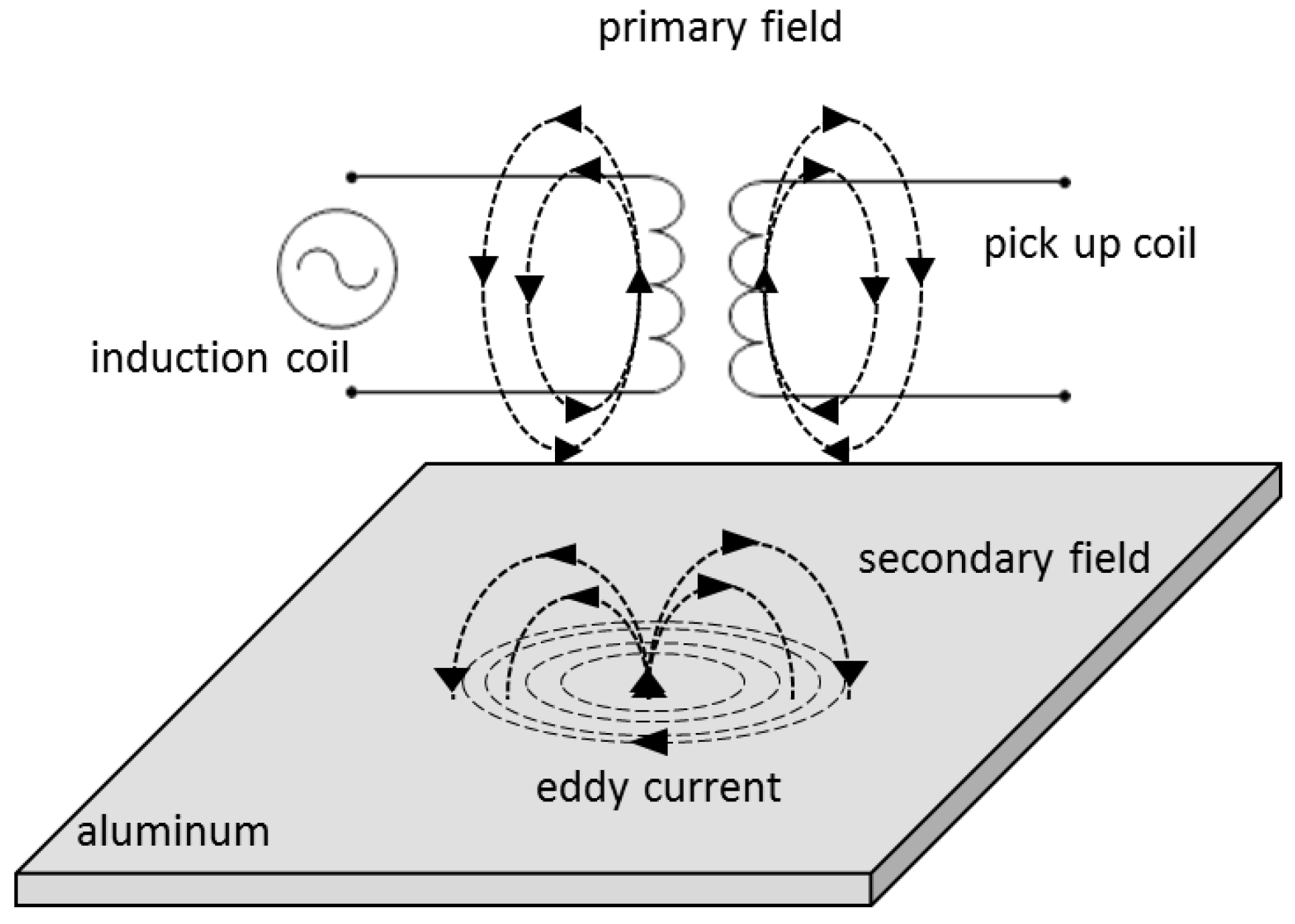
Eddy Current Measurement: Theory
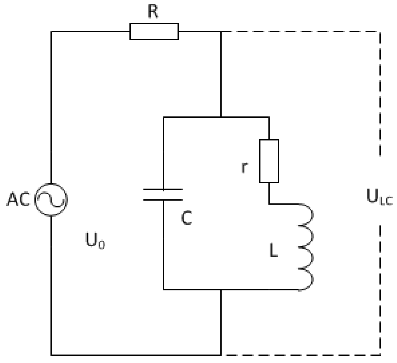
Eddy Current Measurement: Method
Eddy Current Measurement: Practical Aspects and Analyses
3. Methods Overview and Conclusions
Acknowledgments
Author Contributions
Conflicts of Interest
References
- Bichler, C.; Langowski, H.C.; Moosheimer, U.; Bischoff, M. Transparente Aufdampfschichten aus Oxiden von Si, Al und Mg für Barrierepackstoffe. Available online: https://www.mysciencework.com/publication/show/430561f397d6f9ad469136be1369ee3b (accessed on 29 December 2016).
- Pilchik, R. Pharmaceutical blister packaging, Part I. Pharm. Technol. 2000, 24, 68–78. [Google Scholar]
- Dean, D.A.; Evans, E.R.; Hall, I.H. Pharmaceutical Packaging Technology; Taylor & Francis: London, UK, 2005. [Google Scholar]
- Huang, C.C.; Ma, H.W. A multidimensional environmental evaluation of packaging materials. Sci. Total Environ. 2004, 324, 161–172. [Google Scholar] [CrossRef] [PubMed]
- Seshan, K. Handbook of Thin Film Deposition Processes and Techniques; William Andrew: Norwich, NY, USA, 2002. [Google Scholar]
- Mattox, D.M. Physical vapor deposition (PVD) processes. Metal Finish. 2001, 99, 409–423. [Google Scholar] [CrossRef]
- Pierson, H.O. Handbook of Chemical Vapor Deposition: Principles, Technology and Applications; William Andrew: Norwich, NY, USA, 1999. [Google Scholar]
- Leskelä, M.; Ritala, M. Atomic layer deposition (ALD): From precursors to thin film structures. Thin Solid Films 2002, 409, 138–146. [Google Scholar] [CrossRef]
- Hirvikorpi, T.; Vähä-Nissi, M.; Mustonen, T.; Harlin, A.; Iiskola, E.; Karppinen, M. Thin inorganic barrier coatings for packaging materials. In Proceedings of the PLACE 2010 Conference, Albuquerque, NM, USA, 18–21 April 2010.
- Mackenzie, J.D.; Bescher, E.P. Physical properties of sol-gel coatings. J. Sol-Gel Sci. Technol. 2000, 19, 23–29. [Google Scholar] [CrossRef]
- Logothetidis, S.; Laskarakis, A.; Georgiou, D.; Amberg-Schwab, S.; Weber, U.; Noller, K.; Schmidt, M.; Kuecuekpinar-Niarchos, E.; Lohwasser, W. Ultra high barrier materials for encapsulation of flexible organic electronics. Eur. Phys. J. Appl. Phys. 2010, 51, 33203. [Google Scholar] [CrossRef]
- Noller, K.; Mikula, M.; Amberg-Schwab, S.; Weber, U. Multilayer coatings for flexible high-barrier materials. Open Phys. 2009, 7, 371–378. [Google Scholar]
- Brinker, C.J.; Frye, G.C.; Hurd, A.J.; Ashley, C.S. Fundamentals of sol-gel dip coating. Thin Solid Films 1991, 201, 97–108. [Google Scholar] [CrossRef]
- Schultrich, B. Physikalische dampfphasenabscheidung: Bedampfen. In Proceedings of the Surface Engineering und Nanotechnologie SENT, Dresden, Germany, 5–7 December 2006.
- Bishop, C.A. Vacuum Deposition onto Webs, Films and Foils, 2nd ed.; Elsevier: Amsterdam, The Netherlands, 2011. [Google Scholar]
- Mondolfo, L.F. Aluminum Alloys: Structure and Properties; Elsevier: Amsterdam, The Netherlands, 2013. [Google Scholar]
- Ans, J.; Lax, E.; Synowietz, C. Taschenbuch für Chemiker und Physiker; Springer: Berlin/Heidelberg, Germany, 1967. [Google Scholar]
- Hatch, J.E.; Association, A.; Metals, A.S. Aluminum: Properties and Physical Metallurgy; American Society for Metals: Geauga County, OH, USA, 1984. [Google Scholar]
- Kaßmann, M. Grundlagen der Verpackung: Leitfaden für die Fächerübergreifende Verpackungsausbildung; Beuth Verlag: Berlin, Germany, 2014. [Google Scholar]
- Iwakura, K.; Wang, Y.D.; Cakmak, M. Effect of Biaxial Stretching on Thickness Uniformity and Surface Roughness of PET and PPS Films. Int. Polym. Process. 1992, 7, 327–333. [Google Scholar] [CrossRef]
- Cakmak, M.; Wang, Y.; Simhambhatla, M. Processing characteristics, structure development, and properties of uni and biaxially stretched poly (ethylene 2,6 naphthalate)(PEN) films. Polym. Eng. Sci. 1990, 30, 721–733. [Google Scholar] [CrossRef]
- Lin, Y.J.; Dias, P.; Chum, S.; Hiltner, A.; Baer, E. Surface roughness and light transmission of biaxially oriented polypropylene films. Polym. Eng. Sci. 2007, 47, 1658–1665. [Google Scholar] [CrossRef]
- Müller, K.; Schönweitz, C.; Langowski, H.C. Thin Laminate Films for Barrier Packaging Application—Influence of Down Gauging and Substrate Surface Properties on the Permeation Properties. Packag. Technol. Sci. 2012, 25, 137–148. [Google Scholar] [CrossRef]
- Utz, H. Barriereeigenschaften Aluminiumbedampfter Kunststoffolien. Ph.D. Thesis, Technische Universität, Fakultät für Brauwesen, Lebensmitteltechnologie und Milchwissenschaft, Berlin, Germany, 1995. [Google Scholar]
- Kim, C.; Goring, D. Surface morphology of polyethylene after treatment in a corona discharge. J. Appl. Polym. Sci. 1971, 15, 1357–1364. [Google Scholar] [CrossRef]
- Neugebauer, A. Condensation, nucleation, and growth of thin films. In Handbook of Thin Film Technology; Maissel, L.I., Glang, R., Eds.; McGraw-Hill: New York, NY, USA, 1970. [Google Scholar]
- Haefer, R.A. Oberflächen- und Dünnschicht-Technologie; Springer: Berlin, Germany, 1987. [Google Scholar]
- Jacobs, K. H. Frey, G. Kienel. Dünnschichttechnologie. VDI-Verlag GmbH, Düsseldorf 1987. 691 + XVIII pages, numerous figures and tables, 395.00 DM, ISBN 3-18-400670-0. Cryst. Res. Technol. 1989, 24, 1232. [Google Scholar] [CrossRef]
- Vook, R.W. Structure and growth of thin films. Int. Met. Rev. 1982, 27, 209–245. [Google Scholar] [CrossRef]
- Reichelt, K.; Jiang, X. The preparation of thin films by physical vapour deposition methods. Thin Solid Films 1990, 191, 91–126. [Google Scholar] [CrossRef]
- Kern, R.; Metois, G.L. Basic mechanisms in the early stage of epitaxy. Curr. Top. Mater. Sci. 1979, 3, 135–419. [Google Scholar]
- Stoyanov, S. Nucleation theory for high and low supersaturations. Curr. Top. Mater. Sci. 1979, 3, 421–462. [Google Scholar]
- Bravais, A. Abhandlung über Die Systeme von Regelmässig auf Einer Ebene Oder Raum Vertheilten Punkten; Wilhelm Engelmann: Leipzig, Germany, 1897. (In German) [Google Scholar]
- Gottstein, G. Materialwissenschaft und Werkstofftechnik: Physikalische Grundlagen; Springer: Berlin, Germany, 2014. [Google Scholar]
- Weitze, M.D.; Berger, C. Strukturen und Eigenschaften. In Werkstoffe: Unsichtbar, Aber Unverzichtbar; Springer: Berlin, Germany, 2013; pp. 9–66. [Google Scholar]
- Bollmann, W. Crystal Defects and Crystalline Interfaces; Springer Science & Business Media: Berlin, Germany, 2012. [Google Scholar]
- Miesbauer, O.; Schmidt, M.; Langowski, H.C. Stofftransport durch Schichtsysteme aus Polymeren und dünnen anorganischen Schichten. Vak. Forsch. Prax. 2008, 20, 32–40. [Google Scholar] [CrossRef]
- Barker, C.P.; Kochem, K.-H.; Revell, K.M.; Kelly, R.S.A.; Badyal, J.P.S. The Interfacial Chemistry of Metal Oxide Coated and Nanocomposite Coated Polymer Films. Thin Solid Films 1995, 257, 77–82. [Google Scholar] [CrossRef]
- Copeland, N.J.; Astbury, R. Evaporated aluminium on polyester: Optical, Electrical, and Barrier Properties as a Function of Thickness and Time (Part I). In Proceedings of the AIMCAL Technical Conference, Myrtle Beach, SC, USA, 14 October 2010.
- Hass, G.; Scott, N.W. On the structure and properties of some metal and metal oxide films. J. Phys. Radium 1950, 11, 394–402. [Google Scholar] [CrossRef]
- McClure, D.; Struller, C.; Langowski, H.C. Evaporated Aluminium on Polypropylene: Oxide-Layer Thickness as a Function of Oxygen Plasma-Treatment Level. Available online: http://www.aimcal.org/uploads/4/6/6/9/46695933/mcclure_abs.pdf (accessed on 29 December 2016).
- McClure, D.J.; Copeland, N. Evaporated Aluminium on Polyester: Optical, Electrical, and Barrier Properties as a Function of Thickness and Time (Part II). Available online: http://dnn.convertingquarterly.com/magazine/matteucci-awards/id/2420/evaporated-aluminum-on-polyester-optical-electrical-and-barrier-properties-as-a-function-of-thickness-and-time-part-1.aspx (accessed on 29 December 2016).
- Menges, G. Werkstoffkunde der Kunststoffe; Walter de Gruyter: Berlin, Germany, 1971; Volume 2620. [Google Scholar]
- Prins, W.; Hermans, J.J. Theory of Permeation through Metal Coated Polymer Films. J. Phys. Chem. 1959, 63, 716–720. [Google Scholar] [CrossRef]
- Langowski, H.C. Stofftransport durch polymere und anorganische Schichten Transport of Substances through Polymeric and Inorganic Layers. Vak. Forsch. Prax. 2005, 17, 6–13. [Google Scholar] [CrossRef]
- Langowski, H.C.; Utz, H. Dünne anorganische Schichten für Barrierepackstoffe. Int. Z. Lebensm. Technol. Mark. Verpack. Anal. 2002, 9, 522. [Google Scholar]
- Roberts, A.P.; Henry, B.M.; Sutton, A.P.; Grovenor, C.R.; Briggs, G.A.; Miyamoto, T.; Kano, M.; Tsukahara, Y.; Yanaka, M. Gas permeation in silicon oxide/polymer (SiOx/PET) barrier films: Role of oxide lattice, nano-defects and macrodefects. J. Membr. Sci. 2002, 208, 75–88. [Google Scholar] [CrossRef]
- Lohwasser, W. Not only for packaging. In Proceedings of the 43rd Annual Technical Conference of the Society of Vacuum Coaters, Denver, CO, USA, 23–28 April 2000.
- Hanika, M.; Langowski, H.C.; Moosheimer, U.; Peukert, W. Inorganic layers on polymeric films—Influence of defects and morphology on barrier properties. Chem. Eng. Technol. 2003, 26, 605–614. [Google Scholar] [CrossRef]
- Hanika, M. Zur Permeation Durch Aluminiumbedampfte Polypropylen-und Polyethylenterephtalatfolien. Ph.D. Thesis, Technical University of Munich, Munich, Germany, 2004. [Google Scholar]
- Mueller, K.; Weisser, H. Numerical simulation of permeation through vacuum-coated laminate films. Packag. Technol. Sci. 2002, 15, 29–36. [Google Scholar] [CrossRef]
- Rossi, G.; Nulman, M. Effect of local flaws in polymeric permeation reducing barriers. J. Appl. Phys. 1993, 74, 5471–5475. [Google Scholar] [CrossRef]
- Jamieson, E.H.H.; Windle, A.H. Structure and oxygen-barrier properties of metallized polymer film. J. Mater. Sci. 1983, 18, 64–80. [Google Scholar] [CrossRef]
- Bugnicourt, E.; Kehoe, T.; Latorre, M.; Serrano, C.; Philippe, S.; Schmid, M. Recent Prospects in the Inline Monitoring of Nanocomposites and Nanocoatings by Optical Technologies. Nanomaterials 2016, 6, 150. [Google Scholar] [CrossRef]
- Utz, H. Barriereeigenschaften Aluminiumbedampfter Kunststofffolien. Ph.D. Thesis, Technical University of Munich, Munich, Germany, 1995. [Google Scholar]
- Kääriäinen, T.O.; Maydannik, P.; Cameron, D.C.; Lahtinen, K.; Johansson, P.; Kuusipalo, J. Atomic layer deposition on polymer based flexible packaging materials: Growth characteristics and diffusion barrier properties. Thin Solid Films 2011, 519, 3146–3154. [Google Scholar] [CrossRef]
- McCrackin, F.L.; Passaglia, E.; Stromberg, R.R.; Steinberg, H.L. Measurement of the thickness and refractive index of very thin films and the optical properties of surfaces by ellipsometry. J. Res. Natl. Bur. Stand. Phys. Chem. A 1963, 67, 363–377. [Google Scholar] [CrossRef]
- Chatham, H. Oxygen diffusion barrier properties of transparent oxide coatings on polymeric substrates. Surf. Coat. Technol. 1996, 78, 1–9. [Google Scholar] [CrossRef]
- Piegari, A.; Masetti, E. Thin film thickness measurement: A comparison of various techniques. Thin Solid Films 1985, 124, 249–257. [Google Scholar] [CrossRef]
- Pulker, H.K. Thickness measurement, rate control and automation in thin film coating technology. In Proceedings of the 1983 International Techincal Conference, Geneva, Switzerland, 18 April 1983.
- Mattox, D.M. Film characterization and some basic film properties. In Handbook of Physical Vapor Deposition (PVD) Processing; Mattox, D.M., Ed.; William Andrew Publishing: Westwood, NJ, USA, 1998; pp. 569–615. [Google Scholar]
- Martin, P.M. Handbook of Deposition Technologies for Films and Coatings: Science, Applications and Technology; Elsevier: Amsterdam, The Netherlands, 2009. [Google Scholar]
- Juzeliūnas, E. Quartz crystal microgravimetry-fifty years of application and new challenges. Chemija 2009, 20, 218–225. [Google Scholar]
- Zeitvogl, J. Quarzkristallmikrowaage-QCM. Ph.D. Thesis, University of Erlangen-Nuremberg, Erlangen, Germany, 2009. [Google Scholar]
- Frey, H.; Khan, H.R. Handbook of Thin Film Technology; Springer: Berlin, Germany, 2010. [Google Scholar]
- Höpfner, M. Untersuchungen zur Anwendbarkeit der Quarzmikrowaage für Pharmazeutisch Analytische Fragestellungen. Ph.D. Thesis, Martin Luther University of Halle-Wittenberg, Halle, Germany, 2005. [Google Scholar]
- MacLeod, H.A. Thin-Film Optical Filters, 3rd ed.; CRC Press: Cleveland, OH, USA, 2001. [Google Scholar]
- Sauerbrey, G. Verwendung von Schwingquarzen zur Wägung dünner Schichten und zur Mikrowägung. Z. Phys. 1959, 155, 206–222. [Google Scholar] [CrossRef]
- Lu, C.; Czanderna, A.W. Applications of Piezoelectric Quartz Crystal Microbalances; Elsevier: Amsterdam, The Netherlands, 2012. [Google Scholar]
- Thomas, R. Practical Guide to ICP-MS: A Tutorial for Beginners, 2nd ed.; Taylor & Francis: London, UK, 2008. [Google Scholar]
- De Hoffmann, E.; Stroobant, V. Mass Spectrometry: Principles and Applications; Wiley: New York, NY, USA, 2007. [Google Scholar]
- Zoorob, G.K.; McKiernan, J.W.; Caruso, J.A. ICP-MS for elemental speciation studies. Microchim. Acta 1998, 128, 145–168. [Google Scholar] [CrossRef]
- Broekaert, J.A.C. ICP-Massenspektrometrie. In Analytiker-Taschenbuch; Günzler, H., Bahadir, A.M., Danzer, K., Engewald, W., Fresenius, W., Galensa, R., Huber, W., Linscheid, M., Schwedt, G., Tölg, G., Eds.; Springer: Berlin/Heidelberg, Germany, 1988; pp. 127–163. [Google Scholar]
- May, T.W.; Wiedmeyer, R.H. A table of polyatomic interferences in ICP-MS. At. Spectrosc. 1998, 19, 150–155. [Google Scholar]
- Eaton, P.; West, P. Atomic Force Microscopy; Oxford University Press: Oxford, UK, 2010. [Google Scholar]
- Voigtlaender, B. Scanning Probe Microscopy: Atomic Force Microscopy and Scanning Tunneling Microscopy; Springer: Berlin/Heidelberg, Germany, 2015. [Google Scholar]
- Schieferdecker, H.G. Bestimmung Mechanischer Eigenschaften von Polymeren Mittels Rasterkraftmikroskopie; Fakultät für Naturwissenschaften, Universität Ulm: Ulm, Germany, 2005. [Google Scholar]
- Meyer, G.; Amer, N.M. Simultaneous measurement of lateral and normal forces with an optical-beam-deflection atomic force microscope. Appl. Phys. Lett. 1990, 57, 2089–2091. [Google Scholar] [CrossRef]
- Stenzel, O. The Physics of Thin Film Optical Spectra; Springer: Berlin, Germany, 2005. [Google Scholar]
- Bubert, H.; Rivière, J.C.; Arlinghaus, H.F.; Hutter, H.; Jenett, H.; Bauer, P.; Palmetshofer, L.; Fabry, L.; Pahlke, S.; Quentmeier, A.; et al. Surface and Thin-Film Analysis; Wiley Online Library: New York, NY, USA, 2002. [Google Scholar]
- Hertlein, J. Untersuchungen über Veränderungen der Barriereeigenschaften Metallisierter Kunststoffolien Beim Maschinellen Verarbeiten; Utz, Wiss: München, Germany, 1998. [Google Scholar]
- Miller, D.A. Optical Properties of Solid Thin Films by Spectroscopic Reflectometry and Spectroscopic Ellipsometry; ProQuest: Ann Arbor, MI, USA, 2008. [Google Scholar]
- Weiss, J. Einflussfaktoren auf die Barriereeigenschaften metallisierter Folien. Verpak. Rundsch. 1993, 44, 23–28. [Google Scholar]
- Anna, C.; Cosslett, V.E. The optical density and thickness of evaporated carbon films. Br. J. Appl. Phys. 1957, 8, 374–376. [Google Scholar]
- Deb, S.K. Optical and photoelectric properties and colour centres in thin films of tungsten oxide. Philos. Mag. 1973, 27, 801–822. [Google Scholar] [CrossRef]
- Johnson, P.B.; Christy, R.W. Optical Constants of the Noble Metals. Phys. Rev. B 1972, 6, 4370–4379. [Google Scholar] [CrossRef]
- Agar, A.W. The measurement of the thickness of thin carbon films. Br. J. Appl. Phys. 1957, 8, 35–36. [Google Scholar] [CrossRef]
- Moss, T.S. Optical Properties of Tellurium in the Infra-Red. Proc. Phys. Soc. Sec. B 1952, 65, 62–66. [Google Scholar] [CrossRef]
- Lehmuskero, A.; Kuittinen, M.; Vahimaa, P. Refractive index and extinction coefficient dependence of thin Al and Ir films on deposition technique and thickness. Opt. Express 2007, 15, 10744–10752. [Google Scholar] [CrossRef] [PubMed]
- Hass, G.; Waylonis, J.E. Optical constants and reflectance and transmittance of evaporated aluminum in the visible and ultraviolet. JOSA 1961, 51, 719–722. [Google Scholar] [CrossRef]
- Schulz, L.G. The Optical Constants of Silver, Gold, Copper, and Aluminum. I. The Absorption Coefficient k. J. Opt. Soc. Am. 1954, 44, 357–362. [Google Scholar] [CrossRef]
- Heavens, O.S. Optical properties of thin films. Rep. Prog. Phys. 1960, 23, 1–65. [Google Scholar] [CrossRef]
- McMillan, G.K.; Considine, D. Process/Industrial Instruments and Controls Handbook, 5th ed.; McGraw-Hill: New York, NY, USA, 1999. [Google Scholar]
- Pulker, H.K. Einfaches Interferenz-Wechselobjektiv für Mikroskope zur Dickenmessung nach Fizeau-Tolansky. Naturwissenschaften 1966, 53, 224. [Google Scholar] [CrossRef] [PubMed]
- Hanszen, K.J. Der Einfluss von Strukturunregelmässigkeiten beim Zusammenwachsen zweier Aufdampfschichten auf das Schichtdickenmessverfahren mit Hilfe von Vielstrahl-Interferenzen. Thin Solid Films 1968, 2, 509–528. [Google Scholar] [CrossRef]
- Großes Interferenzmikroskop. In Vertriebsabteilung Feinmessgeräte; Carl Zeiss JEAN (Ed.) Druckerei Fortschritt: Jena, Germany, 1965.
- Tippmann, H.; Schawohl, J.; Kups, T. Schichtdickenmessung; TU Ilmenau—Fakultät für Elektrotechnik und Informationstechnik Institut für Werkstofftechnik: Ilmenau, Germany, 2013. [Google Scholar]
- Hammer, A.; Hammer, H.; Hammer, K. Physikalische Formeln und Tabellen; Lindauer: Munich, Germany, 1994. [Google Scholar]
- Pitka, R. Physik: Der Grundkurs; Harri Deutsch Verlag: Frankfurt am Main, Germany, 1999. [Google Scholar]
- Zhigal’skii, G.P.; Jones, B.K. The Physical Properties of Thin Metal Films; CRC Press: Cleveland, OH, USA, 2003; Volume 13. [Google Scholar]
- Liu, H.D.; Zhao, Y.P.; Ramanath, G.; Murarka, S.P.; Wang, G.C. Thickness dependent electrical resistivity of ultrathin (<40 nm) Cu films. Thin Solid Films 2001, 384, 151–156. [Google Scholar]
- Philipp, M. Electrical Transport and Scattering Mechanisms in Thin Silver Films for Thermally Insulating Glazing. Available online: http://www.qucosa.de/fileadmin/data/qucosa/documents/7092/Dissertation_Martin_Philipp.pdf (accessed on 29 December 2016).
- Hoffmann, H.; Vancea, J. Critical-Assessment of Thickness-Dependent Conductivity of Thin Metal-Films. Thin Solid Films 1981, 85, 147–167. [Google Scholar] [CrossRef]
- Leung, K.M. Electrical resistivity of metallic thin films with rough surfaces. Phys. Rev. B 1984, 30, 647–658. [Google Scholar] [CrossRef]
- Ke, Y.; Zahid, F.; Timoshevskii, V.; Xia, K.; Gall, D.; Guo, H. Resistivity of thin Cu films with surface roughness. Phys. Rev. B 2009, 79, 155406. [Google Scholar] [CrossRef]
- Borziak, P.G.; Kulyupin, Y.A.; Nepijko, S.A.; Shamonya, V.G. Electrical conductivity and electron emission from discontinuous metal films of homogeneous structure. Thin Solid Films 1980, 76, 359–378. [Google Scholar] [CrossRef]
- Namba, Y. Resistivity and Temperature Coefficient of Thin Metal Films with Rough Surface. Jpn. J. Appl. Phys. 1970, 9, 1326–1329. [Google Scholar] [CrossRef]
- Darevskii, A.S.; Zhdan, A.G. Real structure and electrical conductivity of island films of metals. Sov. Microelectron. 1978, 7, 356–359. [Google Scholar]
- Bassewitz, A.V. Der Einfluß der Unterlage auf die Struktur und Leitfähigkeit metallischer Aufdampfschichten. Z. Phys. 1967, 201, 350–367. [Google Scholar] [CrossRef]
- Jannesar, M.; Jafari, G.R.; Farahani, S.V.; Moradi, S. Thin film thickness measurement by the conductivity theory in the framework of born approximation. Thin Solid Films 2014, 562, 372–376. [Google Scholar] [CrossRef]
- Palasantzas, G.; Zhao, Y.P.; Wang, G.C.; Lu, T.M.; Barnas, J.; De Hosson, J.T. Electrical conductivity and thin-film growth dynamics. Phys. Rev. B 2000, 61, 11109. [Google Scholar] [CrossRef]
- Munoz, R.C.; Finger, R.; Arenas, C.; Kremer, G.; Moraga, L. Surface-induced resistivity of thin metallic films bounded by a rough fractal surface. Phys. Rev. B 2002, 66, 205401. [Google Scholar] [CrossRef]
- Timalsina, Y.P.; Horning, A.; Spivey, R.F.; Lewis, K.M.; Kuan, T.S.; Wang, G.C.; Lu, T.M. Effects of nanoscale surface roughness on the resistivity of ultrathin epitaxial copper films. Nanotechnology 2015, 26, 075704. [Google Scholar] [CrossRef] [PubMed]
- Ketenoğlu, D.; Ünal, B. Influence of surface roughness on the electrical conductivity of semiconducting thin films. Phys. A Stat. Mech. Appl. 2013, 392, 3008–3017. [Google Scholar] [CrossRef]
- Arenas, C.; Henriquez, R.; Moraga, L.; Muñoz, E.; Munoz, R.C. The effect of electron scattering from disordered grain boundaries on the resistivity of metallic nanostructures. Appl. Surf. Sci. 2015, 329, 184–196. [Google Scholar] [CrossRef]
- Lim, J.W.; Mimura, K.; Isshiki, M. Thickness dependence of resistivity for Cu films deposited by ion beam deposition. Appl. Surf. Sci. 2003, 217, 95–99. [Google Scholar] [CrossRef]
- Zhang, W.; Brongersma, S.H.; Richard, O.; Brijs, B.; Palmans, R.; Froyen, L.; Maex, K. Influence of the electron mean free path on the resistivity of thin metal films. Microelectron. Eng. 2004, 76, 146–152. [Google Scholar] [CrossRef]
- Camacho, J.M.; Oliva, A.I. Surface and grain boundary contributions in the electrical resistivity of metallic nanofilms. Thin Solid Films 2006, 515, 1881–1885. [Google Scholar] [CrossRef]
- Camacho, J.M.; Oliva, A.I. Morphology and electrical resistivity of metallic nanostructures. Microelectron. J. 2005, 36, 555–558. [Google Scholar] [CrossRef]
- Fuchs, K. The conductivity of thin metallic films according to the electron theory of metals. Math. Proc. Camb. Philos. Soc. 1938, 34, 100–108. [Google Scholar] [CrossRef]
- Sondheimer, E.H. The mean free path of electrons in metals. Adv. Phys. 1952, 1, 1–42. [Google Scholar] [CrossRef]
- Soffer, S.B. Statistical Model for the Size Effect in Electrical Conduction. J. Appl. Phys. 1967, 38, 1710–1715. [Google Scholar] [CrossRef]
- Mayadas, A.F.; Shatzkes, M.; Janak, J.F. Electrical resistivity model for polycrystalline films: The case of specular reflection at external surfaces. Appl. Phys. Lett. 1969, 14, 345–347. [Google Scholar] [CrossRef]
- Mayadas, A.F.; Shatzkes, M. Electrical-Resistivity Model for Polycrystalline Films: The Case of Arbitrary Reflection at External Surfaces. Phys. Rev. B 1970, 1, 1382–1389. [Google Scholar] [CrossRef]
- Rider, J.G.; Foxon, C.T.B. An experimental determination of electrical resistivity of dislocations in aluminium. Philos. Mag. 1966, 13, 289–303. [Google Scholar] [CrossRef]
- Mayadas, A.F.; Feder, R.; Rosenberg, R. Resistivity and structure of evaporated aluminum films. J. Vac. Sci. Technol. 1969, 6, 690–693. [Google Scholar] [CrossRef]
- Nakajima, H. Porous Metals with Directional Pores; Springer: Berlin, Germany, 2013. [Google Scholar]
- Lux, F. Models proposed to explain the electrical conductivity of mixtures made of conductive and insulating materials. J. Mater. Sci. 1993, 28, 285–301. [Google Scholar] [CrossRef]
- Siegel, A.C.; Phillips, S.T.; Dickey, M.D.; Lu, N.; Suo, Z.; Whitesides, G.M. Foldable printed circuit boards on paper substrates. Adv. Funct. Mater. 2010, 20, 28–35. [Google Scholar] [CrossRef]
- Parfenov, E.V.; Yerokhin, A.L.; Matthews, A. Impedance spectroscopy characterisation of PEO process and coatings on aluminium. Thin Solid Films 2007, 516, 428–432. [Google Scholar] [CrossRef]
- Dodd, C.V.; Deeds, W.E. Analytical Solutions to Eddy-Current Probe-Coil Problems. J. Appl. Phys. 1968, 39, 2829–2838. [Google Scholar] [CrossRef]
- Hillmann, S.; Heuer, H.; Klein, M. Schichtdicken-Charakterisierung dünner, leitfähiger Schichtsysteme mittels Wirbelstromtechnik. In Proceedings of the DGZfP-Jahrestagung, Erfurt, Germany, 10–12 May 2010.
- Suragus GmbH. EddyCus® TF Lab 4040. Available online: https://www.suragus.com/en/products/thin-film-characterization/sheet-resistance/eddycus-tf-lab-4040/ (accessed on 29 December 2016).
- Fiorillo, F. Measurement and Characterization of Magnetic Materials; Elsevier: Amsterdam, The Netherlands, 2004. [Google Scholar]
- Hillmann, S.; Klein, M.; Heuer, H. In-line thin film characterization using eddy current techniques. Stud. Appl. Electromagn. Mech. 2011, 35, 330–338. [Google Scholar]
- García-Martín, J.; Gómez-Gil, J.; Vázquez-Sánchez, E. Non-destructive techniques based on eddy current testing. Sensors 2011, 11, 2525–2565. [Google Scholar] [CrossRef] [PubMed]
- Singh, S.K. Industrial Instrumentation & Control, 2nd ed.; McGraw-Hill Education: Noida, India, 2003. [Google Scholar]
- Rajotte, R.J. Eddy-current method for measuring the electrical conductivity of metals. Rev. Sci. Instrum. 1975, 46, 743–745. [Google Scholar] [CrossRef]
- Heuer, H.; Hillmann, S.; Roellig, M.; Schulze, M.H.; Wolter, K.J. Thin film characterization using high frequency eddy current spectroscopy. In Proceedings of the 9th IEEE Conference on Nanotechnology (2009 IEEE-NANO), Genoa, Italy, 26–30 July 2009.
- Moulder, J.C.; Uzal, E.; Rose, J.H. Thickness and conductivity of metallic layers from eddy current measurements. Rev. Sci. Instrum. 1992, 63, 3455–3465. [Google Scholar] [CrossRef]
- Angani, C.S.; Ramos, H.G.; Ribeiro, A.L.; Rocha, T.J.; Prashanth, B. Transient eddy current oscillations method for the inspection of thickness change in stainless steel. Sens. Actuators A Phys. 2015, 233, 217–223. [Google Scholar] [CrossRef]
- Qu, Z.; Zhao, Q.; Meng, Y. Improvement of sensitivity of eddy current sensors for nano-scale thickness measurement of Cu films. NDT E Int. 2014, 61, 53–57. [Google Scholar] [CrossRef]
- Mehrabad, M.J.; Ehsani, M.H. An Investigation of Eddy Current, Solid Loss, Induced Voltage and Magnetic Torque in Highly Pure Thin Conductors, Using Finite Element Method. Procedia Mater. Sci. 2015, 11, 412–417. [Google Scholar] [CrossRef]


| Characteristic | Mass Thickness | Geometrical Thickness | Property Thickness | |||||
|---|---|---|---|---|---|---|---|---|
| QCM | ICP-MS | AFM | Eddy Current Measurement | Electrical Resistivity Linear | Electrical Resistivity Squarish | Optical Density | Interference | |
| Measurement range | ++ | +++ | ++ | +++ | +++ | +++ | + | ++ |
| Time needed for one measurement | + | +++ | ++ | + | + | + | + | ++ |
| Non destructive | ✓ | ✗ | ✗ | ✓ | ✗ | ✗ | ✓ | ✗ |
| Punctual measurement | (✓) | ✗ | ✓ | ✓ | ✗ | ✗ | ✓ | ✓ |
| Measurement within multilayer is possible | ✗ | ✓ | (✓) | ✓ | ✗ | ✗ | ✗ | ✗ |
| Impact of pores and defects | ✗ | ✗ | ++ | +++ | +++ | +++ | ++ | ++ |
| Is only metallic aluminum detected? | ✓ | ✗ | ✗ | ✓ | ✓ | ✓ | ✓ | ✓ |
| Usable as inline measurement | ✓ | ✗ | ✗ | ✓ | ✗ | ✗ | ✓ | ✗ |
| Financial invest | + | +++ | +++ | ++ | + | + | + | ++ |
© 2017 by the authors; licensee MDPI, Basel, Switzerland. This article is an open access article distributed under the terms and conditions of the Creative Commons Attribution (CC-BY) license (http://creativecommons.org/licenses/by/4.0/).
Share and Cite
Lindner, M.; Schmid, M. Thickness Measurement Methods for Physical Vapor Deposited Aluminum Coatings in Packaging Applications: A Review. Coatings 2017, 7, 9. https://doi.org/10.3390/coatings7010009
Lindner M, Schmid M. Thickness Measurement Methods for Physical Vapor Deposited Aluminum Coatings in Packaging Applications: A Review. Coatings. 2017; 7(1):9. https://doi.org/10.3390/coatings7010009
Chicago/Turabian StyleLindner, Martina, and Markus Schmid. 2017. "Thickness Measurement Methods for Physical Vapor Deposited Aluminum Coatings in Packaging Applications: A Review" Coatings 7, no. 1: 9. https://doi.org/10.3390/coatings7010009