
Mn-Promoted Growth and Photoluminescence of Molybdenum Disulphide Monolayer

College of Materials & Environmental Engineering, Hangzhou Dianzi University, Hangzhou 310018, China
*
Author to whom correspondence should be addressed.
Coatings 2017, 7(6), 78; https://doi.org/10.3390/coatings7060078
Submission received: 4 May 2017
/
Revised: 5 June 2017
/
Accepted: 6 June 2017
/
Published: 8 June 2017
(This article belongs to the Special Issue Chemical Vapor Deposition)
Abstract
:Molybdenum disulphide (MoS2) monolayer is a two-dimensional semiconductor material with potential applications in nano electronic devices. However, it is still a challenge to reproducibly synthesize single layer MoS2 in high quality. Herein, we report the growth of monolayer of MoS2 on the SiO2/Si substrate with manganese heterogeneous nucleation. It was shown that the Mn promotes the growth of monolayer MoS2 via heterogeneous nucleation. The growth temperature range expanded two-fold, the nucleation density increased as well. The monolayer prepared in the presence of Mn exhibits a unique red emission peak at 732 nm at room temperature compared to the sample in the absence of Mn.
1. Introduction
Molybdenum disulphide (MoS2) monolayer is a direct band gap semiconductor with unique electronic and optical properties. It has many potential applications in electronic, optoelectronic, bionanoelectronic devices, and hydrogen generation [1,2,3,4,5,6]. Due to these promising applications, MoS2 monolayer crystalline has been successfully prepared by vapor deposition on the insulating substrates [7,8,9,10,11]. However, reproducible control of MoS2 growth using the aforementioned methods is still challenging. For example, the atomic ratio of Mo:S and nucleation are out of control. Lee et al. and Ling et al. reported that the nucleation is sensitive to the seeding promoters [12,13]. As we know, MoS2 solid power used as a precursor provides a stoichiometric evaporation of MoS2. Wu et al. are among the first to report vapor deposition (VD) synthesis of MoS2 monolayer using MoS2 as a precursor [9]. The lateral size of MoS2 single crystal is up to 25 µm. Many studies have reported that the underlying metal substrates show great influence on VD-grown MoS2, for example, Cu, Ni, Al, and Ag [14,15]. However, few reports are found on the preparation of MoS2 monolayer with manganese (Mn) as seeding promoter [16]. Herein, we prepared the monolayer of MoS2 on the SiO2/Si substrate pre-coated with a layer of Mn. Monolayer growth was strongly sensitive to the growth temperature and Mn substrate. In addition, the photoluminescence (PL) of the monolayer was greatly influenced by the existence of Mn. Our findings provide a novel technique to synthesize monolayer MoS2 in high quality with improved optical properties.
2. Materials and Methods
MoS2 was prepared by a previously reported vapor deposition (VD) method using a silicon wafer with 300 nm of oxide layer (SiO2/Si) as the substrate [9], as shown in Figure 1a. MoS2 powder (Aladdin, Shanghai, China, 99.5% purity) was used as the precursor. Before use, the precursor (0.5 g) was loaded into a small quartz glass boat (70 mm length) and was put in the center of the tube furnace. Before growth, the precursor was flushed under Ar/H2 (70 sccm, H2 5%, total pressure of 75 Torr. sccm: standard cubic centimeter per minute) for 10 min at room temperature to remove air and water absorbed on the precursor. The substrate was put downstream close to the furnace wall.
For the MoS2 growth, the precursor was heated to 1000 °C from room temperature in 30 min under vacuum (75 Torr, Ar/H2 70 sccm) and kept at 1000 °C for 10 min. Then total pressure was increased to atmospheric pressure before that the carrier gas flow was turned off. After that, the precursor was kept at 1000 °C for 2 h for the MoS2 growth. Afterward, the furnace was turned off and cooled from 1000 °C to room temperature. The vapor of the precursor was introduced to the growth area by Ar/H2 gas flow and deposited onto the substrate. The temperature of the area ranged from 710 to 850 °C.
For the Mn substrate preparation, Mn metal powder (Aladdin, 99.9% purity) was used as the precursor. The precursor (2.0 g) was loaded onto a small quartz glass boat (70 mm length) and was put in the center of the tube furnace. The silicon wafer with oxide layer (SiO2/Si) used as the substrate was put downstream close to the furnace wall. Mn metal power was heated to 900 °C from room temperature in 30 min and kept at 900 °C for 90 min under vacuum (75 Torr, Ar/H2 70 sccm). Mn metal was evaporated and deposited onto the SiO2/Si substrate.
The temperature of the MoS2 growth area was obtained indirectly. First, we ran a blank test and obtained the temperature distribution inside the furnace, and plotted the temperature distribution curve in respect to the heat position as a reference. For the blank test, the furnace center temperature was kept at 1000 °C. Then we confirmed the position where the sample had been loaded and checked with the temperature distribution curve in that position. In this way, we obtained the accurate growth temperature of the MoS2 and the uncertainty of the measurement is mainly from the measurement of the position of the sample. As shown in Figure 1b, the growth temperature (T) vs. position (x) shows a linear function of T = 795.7 − 6.3x in the temperature range 665–856 °C. The origin of the x-coordinate is chosen in the center of the sample. The positive direction of X-axis is along the gas flow direction. The absolute error of position was ±1 mm. Therefore, the absolute error of the growth temperature is ca. ±6 °C.
Optical microscope imaging of the sample was conducted with a Jiangnan MV3000 digital microscope (Nanjing jiangnan Novel Optics Co., Ltd., Nanjing, China). Tapping mode atomic force microscopy was performed on an Agilent 5500 (Palo Alto, CA, USA) in air. Raman spectrum and photoluminescence were acquired on a Renishaw inVia micro-Raman spectroscope (Renishaw, London, UK) with a 532 nm solid state laser at room temperature.
3. Results and Discussion
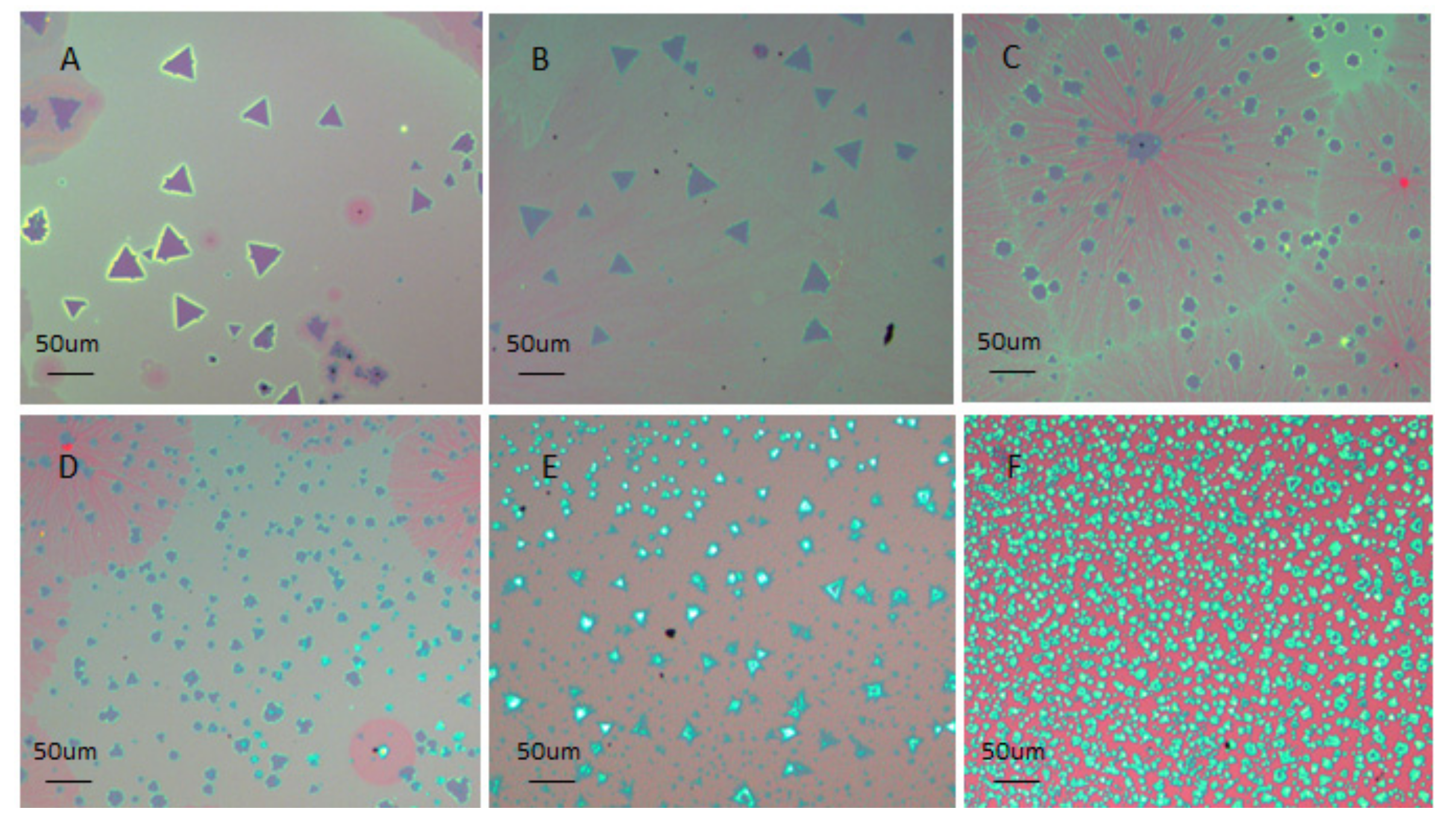
To investigate the growth behavior of MoS2 with or without Mn seeding promoter, we used two methods to prepare MoS2. The difference lied in the substrate that treated with or without Mn vapor. In the first method, the MoS2 was grown on the bare SiO2/Si substrate. In the second method, Mn metal was evaporated at 900 °C for 90 min under vacuum (75 Torr, Ar/H2 70 sccm) onto the SiO2/Si substrate (Mn/SiO2/Si) before the MoS2 growth. Optical images of the MoS2 film were shown inFigure 2 and Figure 3. MoS2 monolayer domains were only found on the higher temperature region of the substrate. The growth temperature ranged from ca. 780 to 725 °C for the SiO2/Si substrate, while it was about 855–730 °C for the Mn/SiO2/Si substrate. The range of growth temperature was about two times wider for Mn catalyzed MoS2 growth, compared to that without the existence of Mn. It also can be observed that the domain size increases with the increase of the temperature in both samples. The largest size (ca. 140 µm) was obtained at about 770 °C on the SiO2/Si substrate.
Meanwhile, the shape becomes a regular triangle at elevated temperature Figure 2A–D and Figure 3A,B, indicating that these domains are of high crystallinity. In addition, the optical images of these domains in Figure 2A–D and Figure 3A,B show a uniform color contrast on the substrate, suggesting high thickness uniformity of the MoS2 domain.
The optical contrast of the particles grown at lower temperature (Figure 3E,F) indicates that the MoS2 multi-layers are formed. The density of the domain or particles on the Mn/SiO2/Si substrate is greater than that on the SiO2/Si substrate. These results are in agreement with our hypothesis that Mn promotes heterogeneous nucleation of MoS2 during the growth.
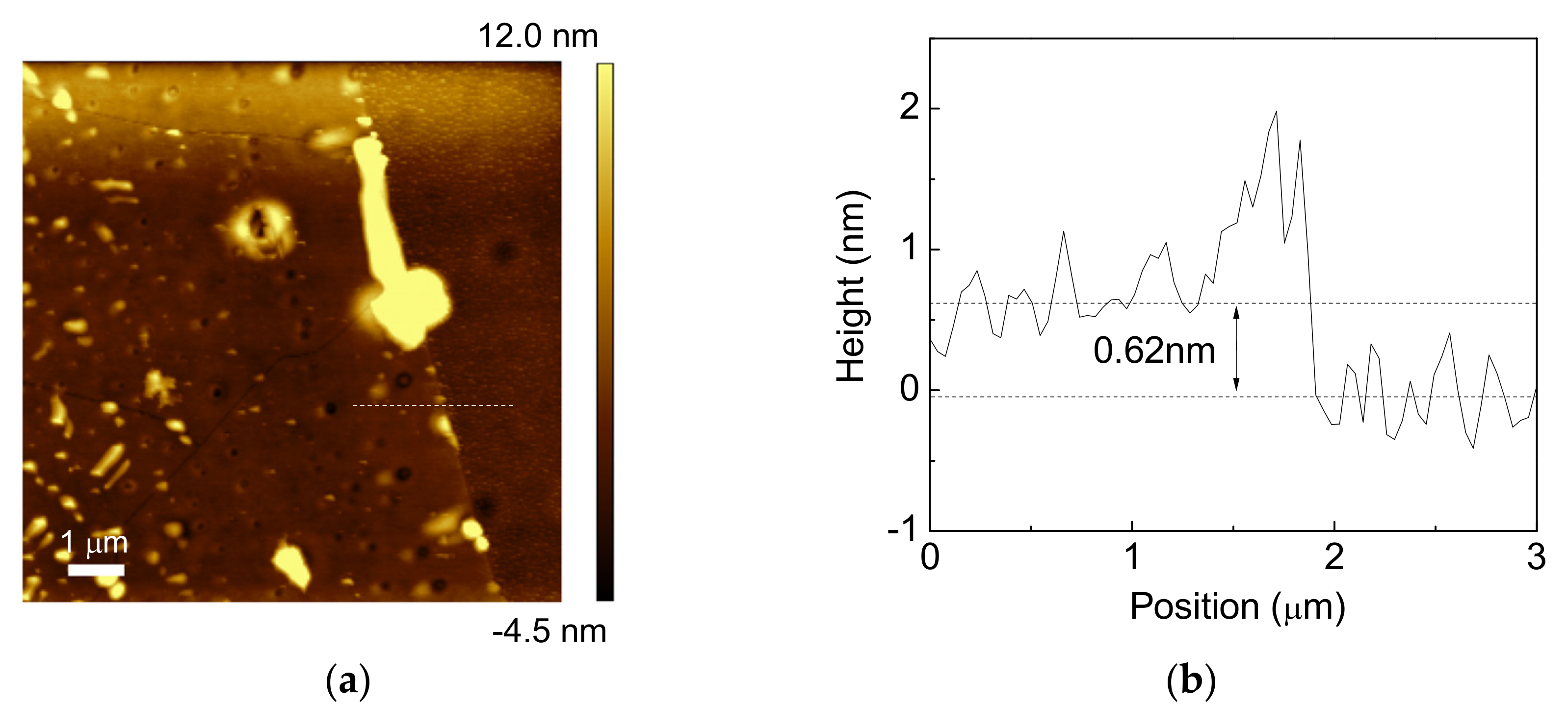
Typical AFM image of the MoS2 domain grown on the SiO2/Si at 760 °C is shown in Figure 4. The thickness of the MoS2 domain 0.62 ± 0.1 nm (Figure 3), is consistent with the reported value of monolayer film [17,18], indicating that the MoS2 domain is monolayer.
Figure 5 displays the typical Raman spectra of monolayer MoS2 triangular domain corresponded to the images in Figure 2C and Figure 3B, respectively. The frequency difference between the E2g and A1g modes of MoS2 is conveniently used for rapid and accurate determination of the thickness of MoS2. The frequency difference of the monolayer MoS2 is ca. 20 cm−1 [13,19]. The E2g and A1g modes of MoS2 are located at 384.7 and 404.6 cm−1 for the sample grown on bare SiO2/Si substrate, with a frequency difference of 19.9 cm−1 between these two modes, In comparison, MoS2 grown in the presence of Mn demonstrates a frequency difference of 21.7 cm−1, locating at a Raman shift of 382.4 cm−1 and 404.1 cm−1, respectively. The frequency difference value in both samples consisted with the value of monolayer MoS2, confirming the successful preparation of MoS2 monolayer [13,19]. We observed that the peak positions of the sample prepared in the presence of Mn catalyst are red shifted compared to those grown on the bare SiO2/Si substrate. Besides the red shift, a shoulder right to the defect-related 2LA (M) Raman band was also observed [19]. It is possible that the red shift and the shoulder are caused by Mn seeding promoter inducing strain defects during the growth of MoS2, such as the heterogeneous nucleating.
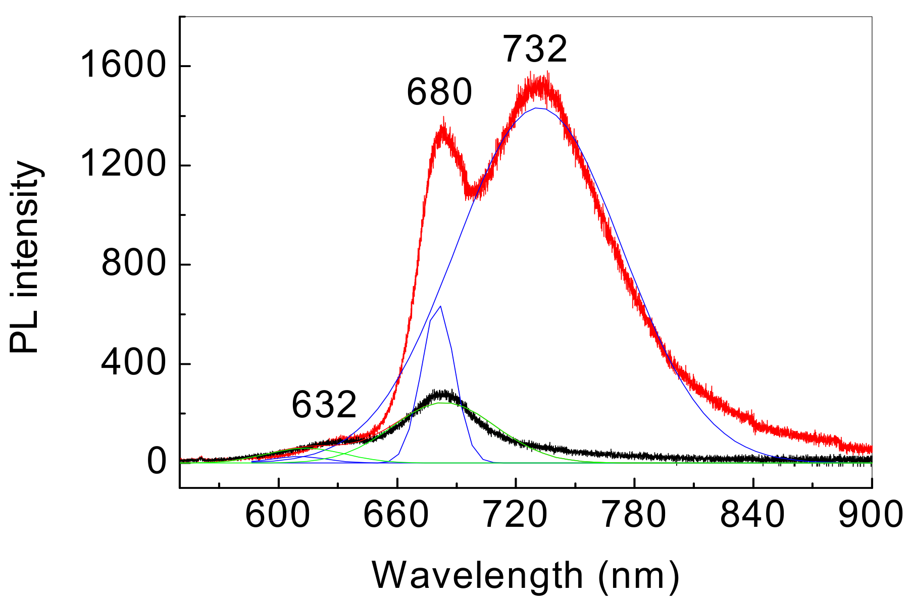
In contrast to multi-layer or bulk MoS2, the optical bandgap of monolayer MoS2 is direct. Under photon excitation, strong PL emission will be found in monolayer MoS2. Figure 6 shows the typical photoluminescence spectra (PL) of the monolayer MoS2 triangular domain corresponded to the images in panel C of Figure 2 and panel B of Figure 3, respectively. The excitation wavelength was 532 nm. The PL peak at ca. 680 nm (1.82 eV) and 632 nm (1.96 eV) are attributed to the A1 and B1 direct excitonic transition emission of MoS2 monolayer [11,17,20]. The PL peaks were fitted with Gaussian curves. The full width at half maximum (FWHM) of the peak at ca. 680 nm is 52.3 ± 0.3 nm for the sample grown on SiO2/Si substrate, and 16.5 ± 0.2 nm for the sample grown on Mn/SiO2/Si substrate. The strong PL intensity and reduced FWHM at 680 nm indicate that the high quality of the monolayer of MoS2 was successfully prepared on the Mn/SiO2/Si substrate. We interpret the strong PL peak intensity and reduced FWHM at 680 nm are concerned with the heterogeneous nucleation of MoS2. Ling et al. recently studied the MoS2 monolayer growth using seeding promoter [13]. They found that the seeding promoter played a major role in the nucleation and even the domain quality of the MoS2.
Besides the peak at 680 nm, an unexpected stronger and broader low energy peak centered at 732 nm (1.69 eV) with a FWHM of 70.0 nm was observed at room temperature in the sample grown on the Mn/SiO2/Si substrate. This peak may be produced by the recombination of defect-bound excitons. Tongay et al. observed a defect-induced bound exciton peak at ca. 1.78 eV, and the peak disappeared as the temperature is higher than 250 K [21]. Here it is possible that the strain-induced defects were formed during the heterogeneous nucleation, resulting in emission at 732 nm at room temperature. Detailed studies of the peak will be reported in future work.
4. Conclusions
In summary, we have successfully prepared high quality monolayer MoS2 with regular triangular morphology and high thickness uniformity by VD method on SiO2/Si substrate with/without a coating layer of Mn as seeding promoters. The growth of MoS2 is highly sensitive to the temperature. The results reveal that the MoS2 growth is limited to a specific temperature range, and the range is expanded two-fold in the presence of Mn. In addition, we also found the nucleation density was increased on the substrate with Mn seeding promoter. Both the Raman and PL spectra revealed that the MoS2 domain grown at elevated temperature is monolayer. The PL spectra of the monolayer showed A1 excitation emission at 680 nm, while a unique and strong emission at 732 nm was obtained for the monolayer MoS2 prepared in the presence of Mn.
Acknowledgments
This work was supported by Natural Science Foundation of Zhejiang Province, China Projects (LY16E020008), and Chinese NSF Projects (61106100).
Author Contributions
Shengzhong Jin designed and performed the experiments; Jiaxin Weng performed the experiments; Shichao Zhao and Yanfei Lv analyzed the data and wrote the paper.
Conflicts of Interest
The authors declare no conflict of interest.
References
- Mak, K.F.; Lee, C.; Hone, J.; Shan, J.; Heinz, T.F. Atomically Thin MoS2: A new direct-gap semiconductor. Phys. Rev. Lett. 2010, 105, 136805:1–136805:4. [Google Scholar] [CrossRef] [PubMed]
- Jariwala, D.; Sangwan, V.K.; Lauhon, L.J.; Marks, T.J.; Hersam, M.C. Emerging device applications for semiconducting two-dimensional transition metal dichalcogenides. ACS Nano 2014, 8, 1102–1120. [Google Scholar] [CrossRef] [PubMed]
- Hayamizu, Y.; So, C.R.; Dag, S.; Page, T.S.; Starkebaum, D.; Sarikaya, M. Bioelectronic interfaces by spontaneously organized peptides on 2D atomic single layer materials. Sci. Rep. 2016, 6, 33778:1–33778:9. [Google Scholar] [CrossRef] [PubMed]
- Gan, X.R.; Zhao, H.M.; Quan, X. Two-dimensional MoS2: A promising building block for biosensors. Biosens. Bioelectron. 2017, 89, 56–71. [Google Scholar] [CrossRef] [PubMed]
- Mak, K.F.; Shan, J. Photonics and optoelectronics of 2D semiconductor transition metal dichalcogenides. Nat. Photonics 2016, 10, 216–226. [Google Scholar] [CrossRef]
- Ma, S.; Xie, J.; Wen, J.Q.; He, K.L.; Li, X.; Liu, W.; Zhang, X.C. Constructing 2D layered hybrid CdS nanosheets/MoS2 heterojunctions for enhanced visible-light photocatalytic H2 generation. Appl. Surf. Sci. 2017, 391, 580–591. [Google Scholar] [CrossRef]
- Van Der Zande, A.M.; Huang, P.Y.; Chenet, D.A.; Berkelbach, T.C.; You, Y.M.; Lee, G.H.; Heinz, T.F.; Reichman, D.R.; Muller, D.A.; Hone, J.C. Grains and grain boundaries in highly crystalline monolayer molybdenum disulphide. Nat. Mater. 2013, 12, 554–561. [Google Scholar] [CrossRef] [PubMed]
- Xie, Y.; Wang, Z.; Zhan, Y.J.; Zhang, P.; Wu, R.X.; Jiang, T.; Wu, S.W.; Wang, H.; Zhao, Y.; Nan, T.; et al. Controllable growth of monolayer MoS2 by chemical vapor deposition via close MoO2 precursor for electrical and optical applications. Nanotechnology 2017, 28, 084001:1–084001:11. [Google Scholar] [CrossRef] [PubMed]
- Wu, S.F.; Huang, C.M.; Aivazian, G.; Ross, J.S.; Cobden, D.H.; Xu, X.D. Vapor-solid growth of high optical quality MoS2 monolayers with near-unity valley polarization. ACS Nano 2013, 7, 2768–2772. [Google Scholar] [CrossRef] [PubMed]
- Luo, S.W.; Qi, X.; Ren, L.; Hao, G.L.; Fan, Y.P.; Liu, Y.D.; Han, W.J.; Zang, C.; Li, J.; Zhong, J.X. Photoresponse properties of large-area MoS2 atomic layer synthesized by vapor phase deposition. J. Appl. Phys. 2014, 116, 164304:1–164304:6. [Google Scholar] [CrossRef]
- Kim, Y.; Bark, H.; Ryu, G.H.; Lee, Z.; Lee, C. Wafer-scale monolayer MoS2 grown by chemical vapor deposition using a reaction of MoO3 and H2S. J. Phys. Condens. Matter 2016, 28, 184002:1–184002:6. [Google Scholar] [CrossRef] [PubMed]
- Lee, Y.H.; Zhang, X.Q.; Zhang, W.J.; Chang, M.T.; Lin, C.T.; Chang, K.D.; Yu, Y.C.; Wang, J.T.W.; Chang, C.S.; Li, L.J.; et al. Synthesis of large-area MoS2 atomic layers with chemical vapor deposition. Adv. Mater. 2012, 24, 2320–2325. [Google Scholar] [CrossRef] [PubMed]
- Ling, X.; Lee, Y.H.; Lin, Y.X.; Fang, W.J.; Yu, L.L.; Dresselhaus, M.S.; Kong, J. Role of the seeding promoter in MoS2 growth by chemical vapor deposition. Nano Lett. 2014, 14, 464–472. [Google Scholar] [CrossRef] [PubMed]
- Loh, T.A.J.; Chua, D.H.C. Growth mechanism of pulsed laser fabricated few-layer MoS2 on metal substrates. ACS Appl. Mater. Interface 2014, 6, 15966–15971. [Google Scholar] [CrossRef] [PubMed]
- Loh, T.A.J.; Tanemura, M.; Chua, D.H.C. Ultrathin MoS2 and WS2 layers on silver nano-tips as electron emitters. Appl. Phys. Lett. 2016, 109, 133102. [Google Scholar] [CrossRef]
- Zhang, K.H.; Feng, S.M.; Wang, J.J.; Azcatl, A.L.; Lu, N.; Addou, R.; Wang, N.; Zhou, C.J.; Lerach, J.; Bojan, V.; et al. Manganese doping of Monolayer MoS2: The substrate is critical. Nano Lett. 2015, 15, 6586–6591. [Google Scholar] [CrossRef] [PubMed]
- Wang, S.S.; Rong, Y.M.; Fan, Y.; Pacios, M.; Bhaskaran, H.; He, K.; Warner, J.H. Shape evolution of monolayer MoS2 crystals grown by chemical vapor deposition. Chem. Mater. 2014, 26, 6371–6379. [Google Scholar] [CrossRef]
- Amani, M.; Chin, M.L.; Birdwell, A.G.; O’Regan, T.P.; Najmaei, S.; Liu, Z.; Ajayan, P.M.; Lou, J.; Dubey, M. Electrical performance of monolayer MoS2 field-effect transistors prepared by chemical vapor deposition. Appl. Phys. Lett. 2013, 102, 193107:1–193107:4. [Google Scholar] [CrossRef]
- Mignuzzi, S.; Pollard, A.J.; Bonini, N.; Brennan, B.; Gilmore, I.S.; Pimenta, M.A.; Richards, D.; Roy, D. Effect of disorder on Raman scattering of single-layer MoS2. Phys. Rev. B 2015, 91, 195411:1–195411:7. [Google Scholar] [CrossRef]
- Splendiani, A.; Sun, L.; Zhang, Y.B.; Li, T.S.; Kim, J.; Chim, C.Y.; Galli, G.; Wang, F. Emerging photoluminescence in monolayer MoS2. Nano Lett. 2010, 10, 1271–1275. [Google Scholar] [CrossRef] [PubMed]
- Tongay, S.; Suh, J.; Ataca, C.; Fan, W.; Luce, A.; Kang, J.S.; Liu, J.; Ko, C.; Raghunathanan, R.; Zhou, J.; et al. Defects activated photoluminescence in two-dimensional semiconductors: Interplay between bound, charged, and free excitons. Sci. Rep. 2013, 3, 2657:1–2657:5. [Google Scholar] [CrossRef] [PubMed]
Figure 1.
(a) Schematic of the MoS2 growth setup; (b) Plot of temperature vs. position near the MoS2 growth area, and the linear fit of the data. The origin of the x-coordinate is chosen in the center of the sample. The positive direction of x-axis is along the gas flow direction.
Figure 1.
(a) Schematic of the MoS2 growth setup; (b) Plot of temperature vs. position near the MoS2 growth area, and the linear fit of the data. The origin of the x-coordinate is chosen in the center of the sample. The positive direction of x-axis is along the gas flow direction.
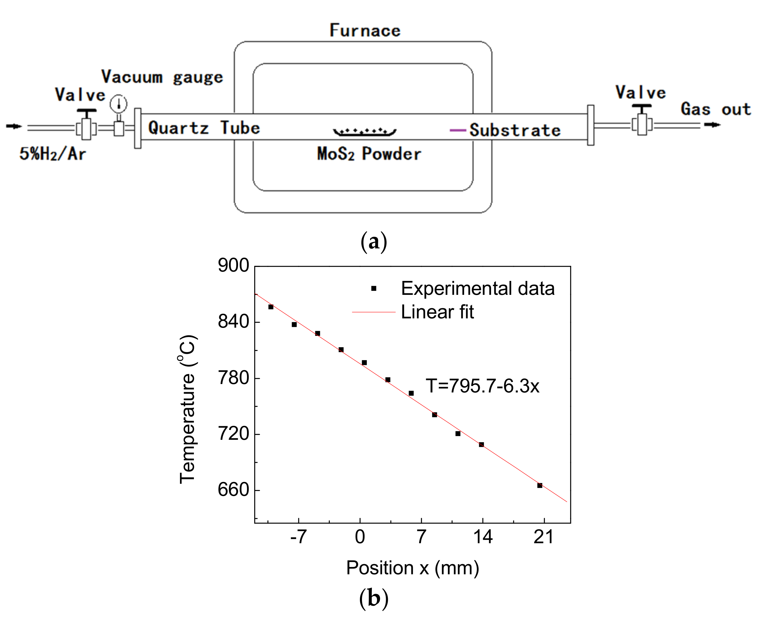
Figure 2.
The optical images of the MoS2 flakes grown on SiO2/Si substrate with different temperatures: (A) 780 °C, (B) 770 °C, (C) 760 °C, (D) 750 °C, (E) 736 °C, and (F) 725 °C.
Figure 2.
The optical images of the MoS2 flakes grown on SiO2/Si substrate with different temperatures: (A) 780 °C, (B) 770 °C, (C) 760 °C, (D) 750 °C, (E) 736 °C, and (F) 725 °C.
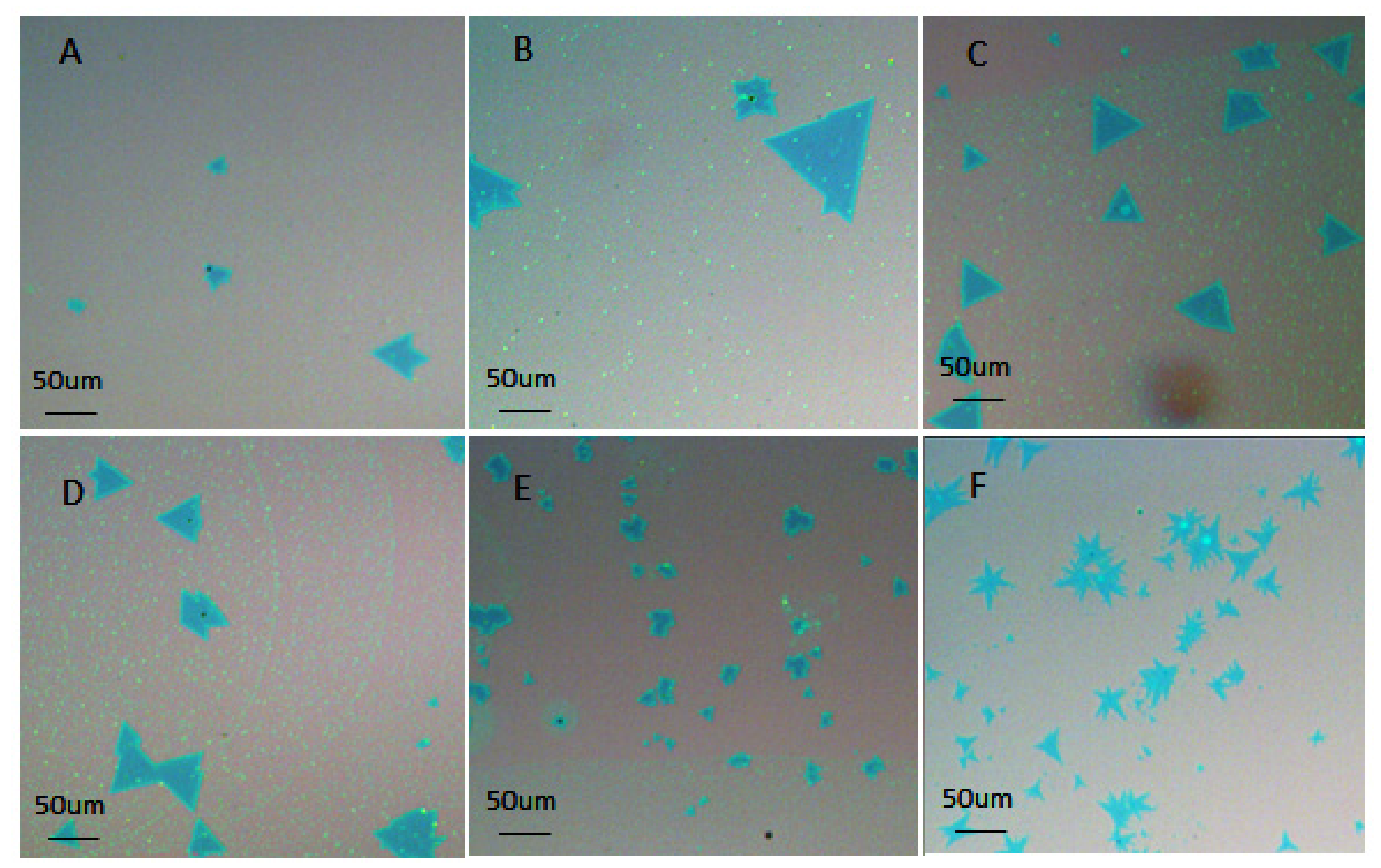
Figure 3.
The optical images of the MoS2 flakes grown on Mn/SiO2/Si substrate with different temperatures: (A) 855 °C, (B) 837 °C, (C) 828 °C, (D) 812 °C, (E) 749 °C, and (F) 730 °C.
Figure 3.
The optical images of the MoS2 flakes grown on Mn/SiO2/Si substrate with different temperatures: (A) 855 °C, (B) 837 °C, (C) 828 °C, (D) 812 °C, (E) 749 °C, and (F) 730 °C.

Figure 4.
AFM image and cross section of MoS2 grown on a SiO2/Si substrate. The line indicates the location where the cross section was determined. Scale bar in the AFM image represents 1 µm. (a) AFM; (b) Cross section of the marked area in (a).
Figure 4.
AFM image and cross section of MoS2 grown on a SiO2/Si substrate. The line indicates the location where the cross section was determined. Scale bar in the AFM image represents 1 µm. (a) AFM; (b) Cross section of the marked area in (a).

Figure 5.
Typical Raman spectra of MoS2 samples grown on Mn/SiO2/Si substrate (red line) and SiO2/Si substrate (black line), respectively.
Figure 5.
Typical Raman spectra of MoS2 samples grown on Mn/SiO2/Si substrate (red line) and SiO2/Si substrate (black line), respectively.
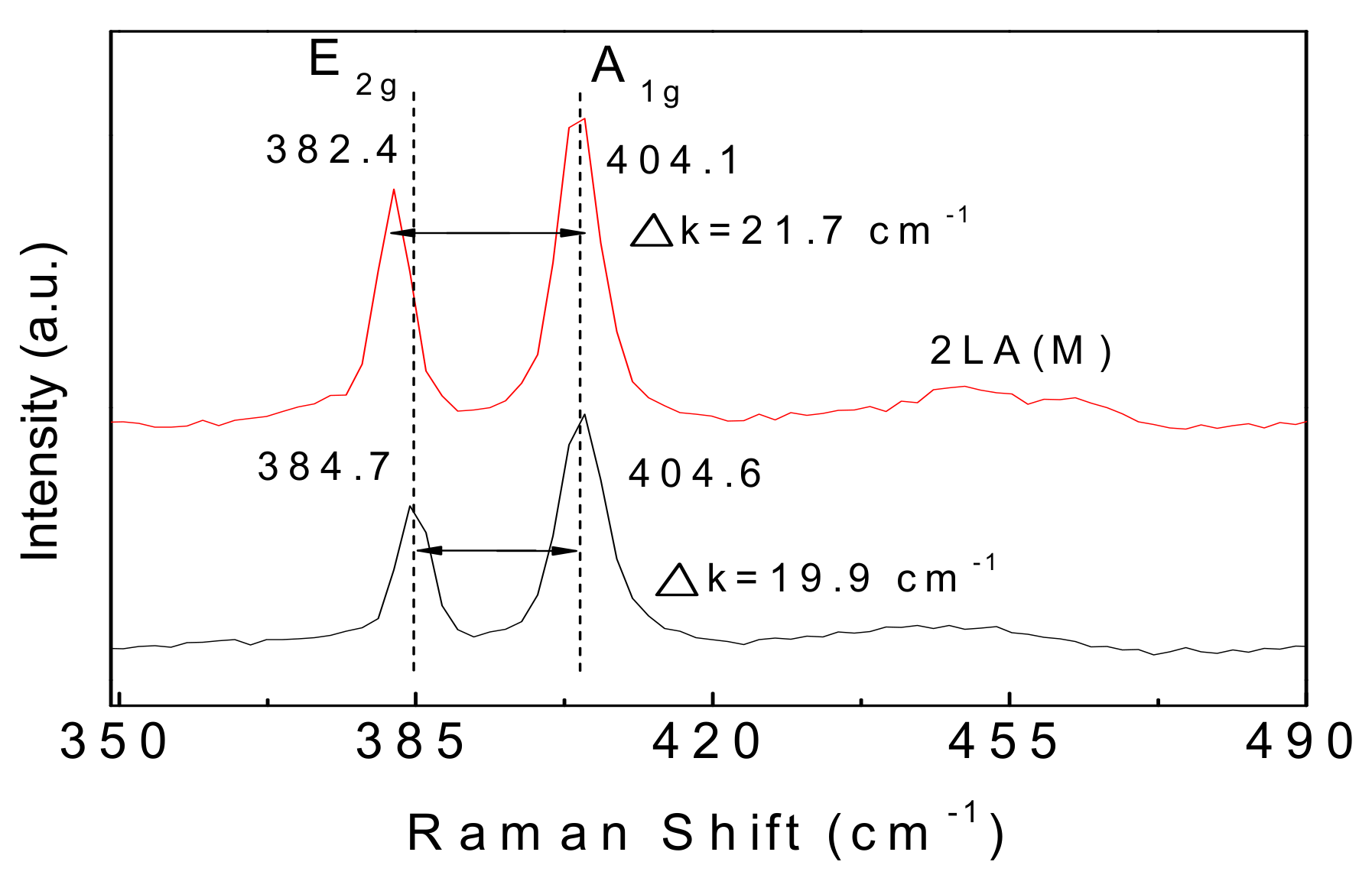
Figure 6.
Typical PL spectra of MoS2 samples grown on Mn/SiO2/Si substrate (red line) and SiO2/Si substrate (black line), respectively. Green lines are the Gaussian fit to the black line, and blue lines are the Gaussian fit to the red line.
Figure 6.
Typical PL spectra of MoS2 samples grown on Mn/SiO2/Si substrate (red line) and SiO2/Si substrate (black line), respectively. Green lines are the Gaussian fit to the black line, and blue lines are the Gaussian fit to the red line.
© 2017 by the authors. Licensee MDPI, Basel, Switzerland. This article is an open access article distributed under the terms and conditions of the Creative Commons Attribution (CC BY) license (http://creativecommons.org/licenses/by/4.0/).
Share and Cite
MDPI and ACS Style
Jin, S.; Zhao, S.; Weng, J.; Lv, Y. Mn-Promoted Growth and Photoluminescence of Molybdenum Disulphide Monolayer. Coatings 2017, 7, 78. https://doi.org/10.3390/coatings7060078
AMA Style
Jin S, Zhao S, Weng J, Lv Y. Mn-Promoted Growth and Photoluminescence of Molybdenum Disulphide Monolayer. Coatings. 2017; 7(6):78. https://doi.org/10.3390/coatings7060078
Chicago/Turabian StyleJin, Shengzhong, Shichao Zhao, Jiaxin Weng, and Yanfei Lv. 2017. "Mn-Promoted Growth and Photoluminescence of Molybdenum Disulphide Monolayer" Coatings 7, no. 6: 78. https://doi.org/10.3390/coatings7060078
Note that from the first issue of 2016, this journal uses article numbers instead of page numbers. See further details here.