2D Materials-Coated Plasmonic Structures for SERS Applications


Abstract
1. Introduction
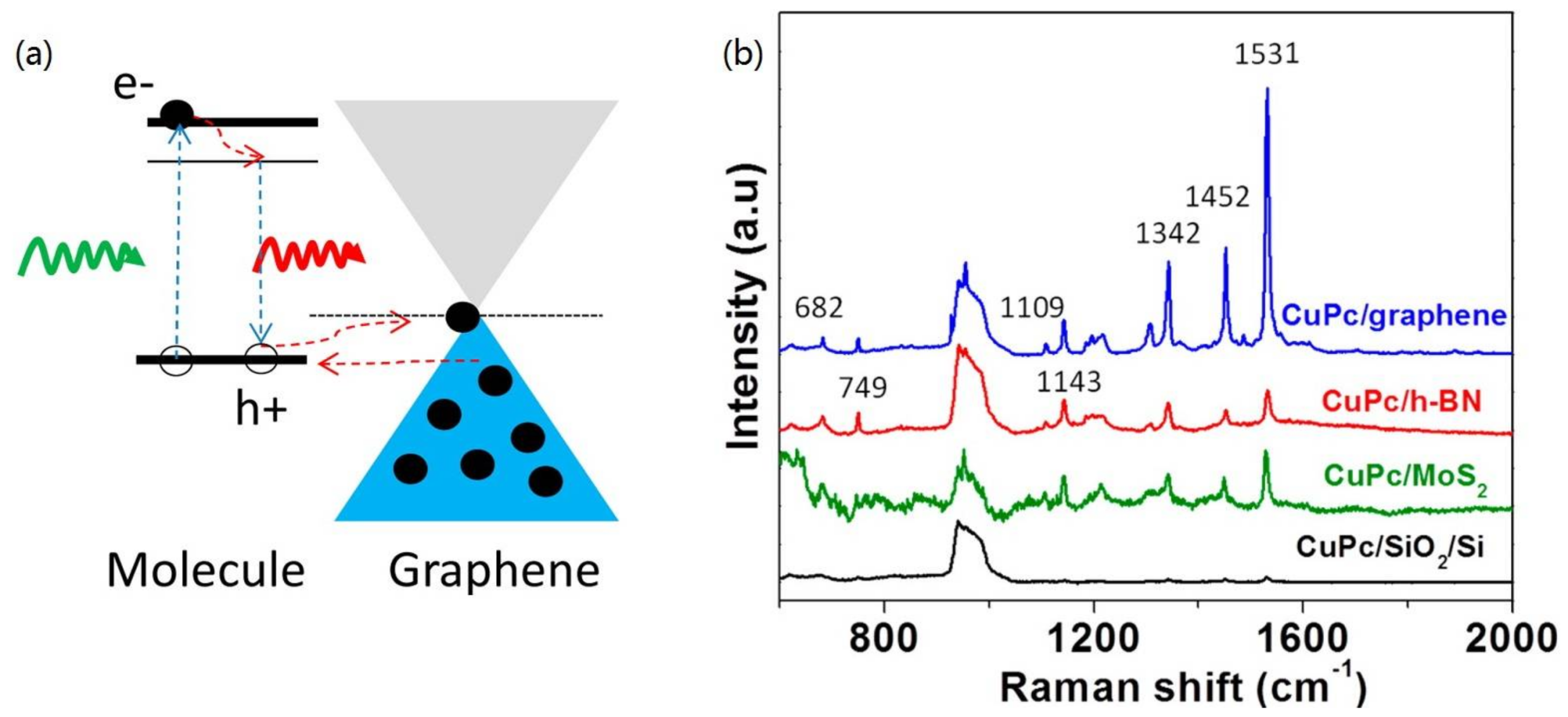
2. Raman Enhancement of 2D Materials
3. Two Dimensional Materials-Coated Plasmonic Nanostructures
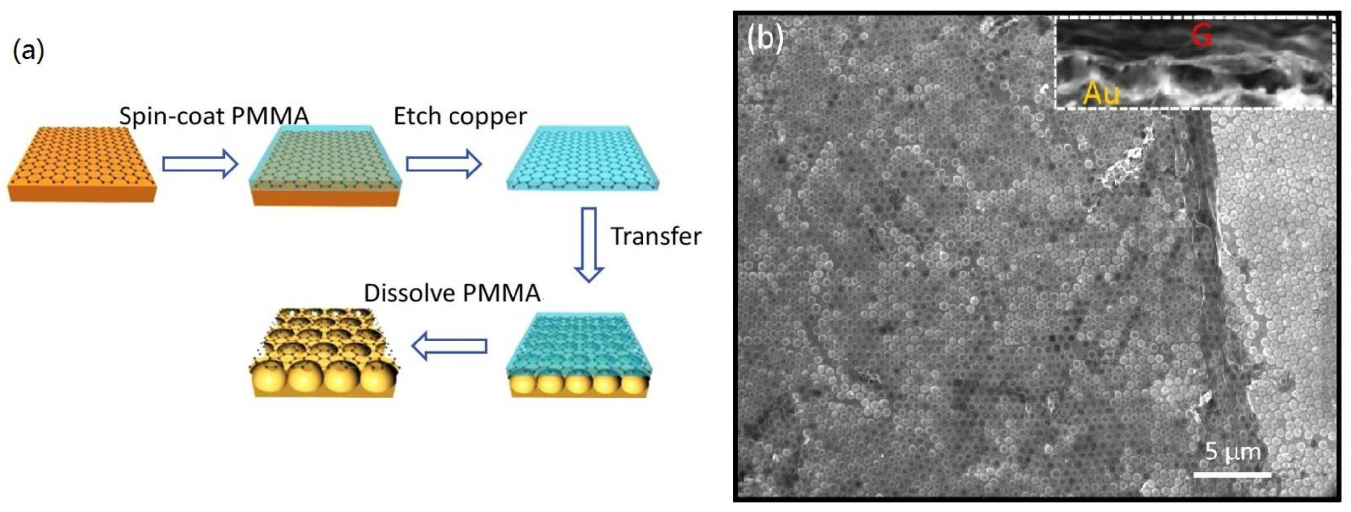
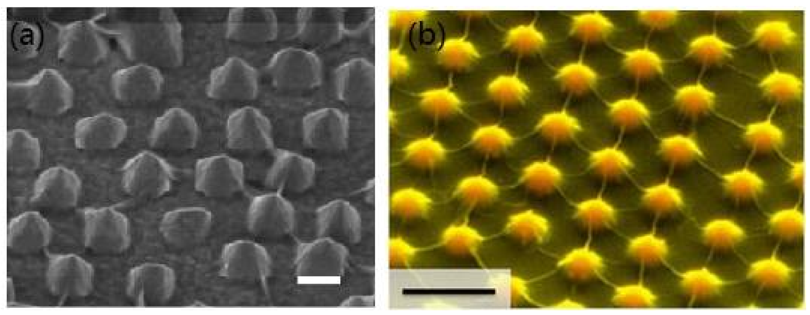
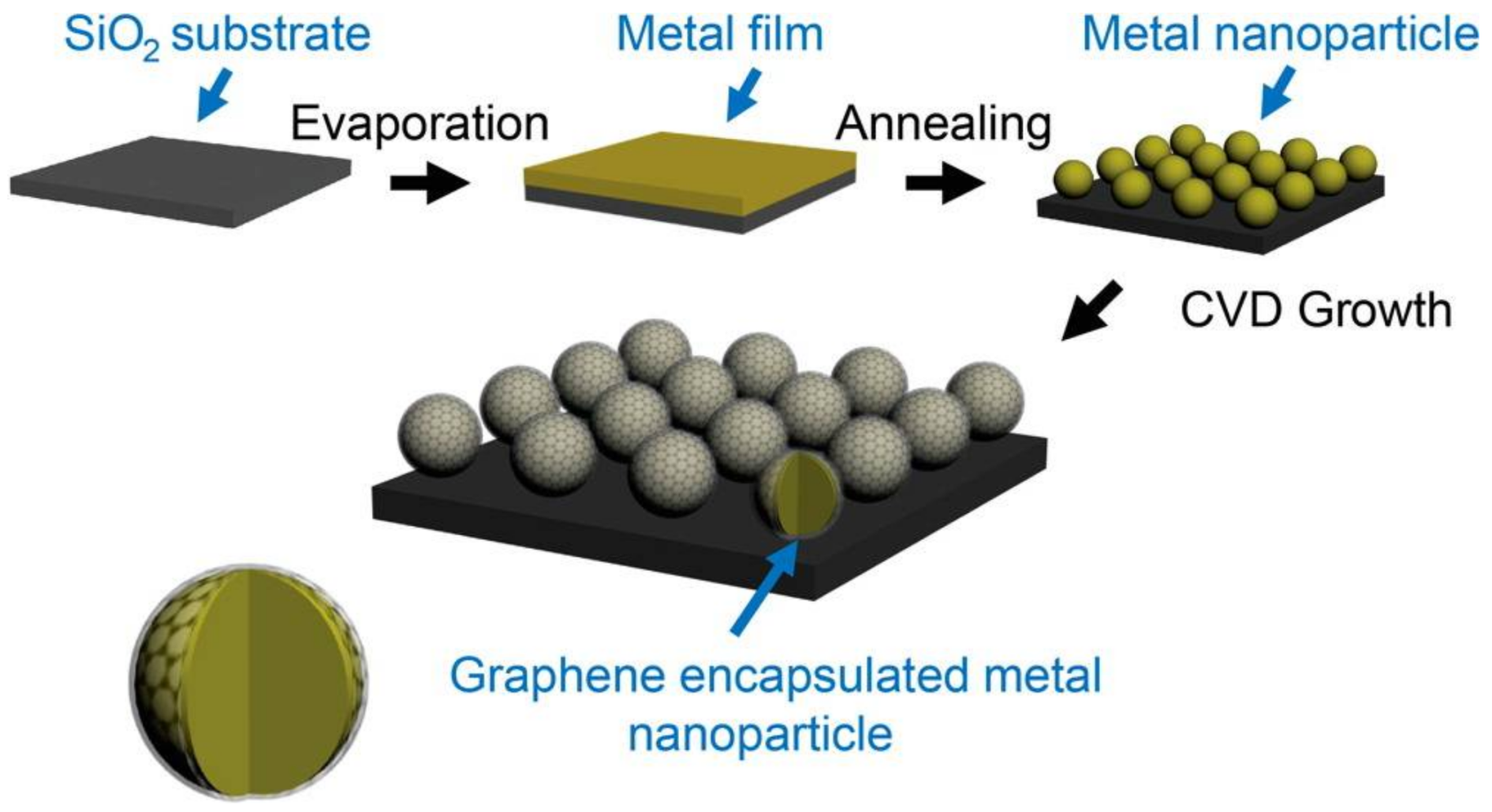
3.1. Fabrication
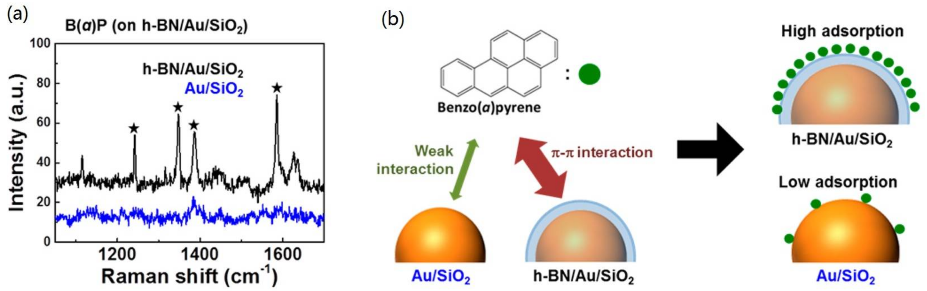
3.2. Sensitivity
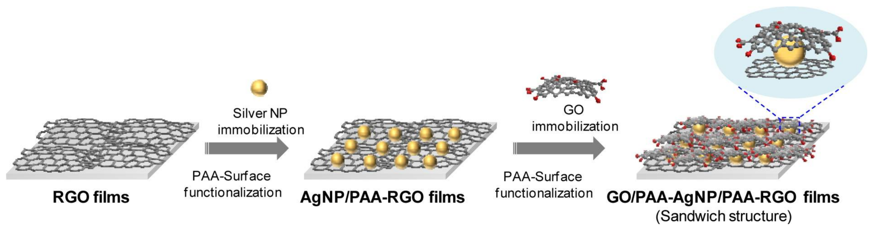
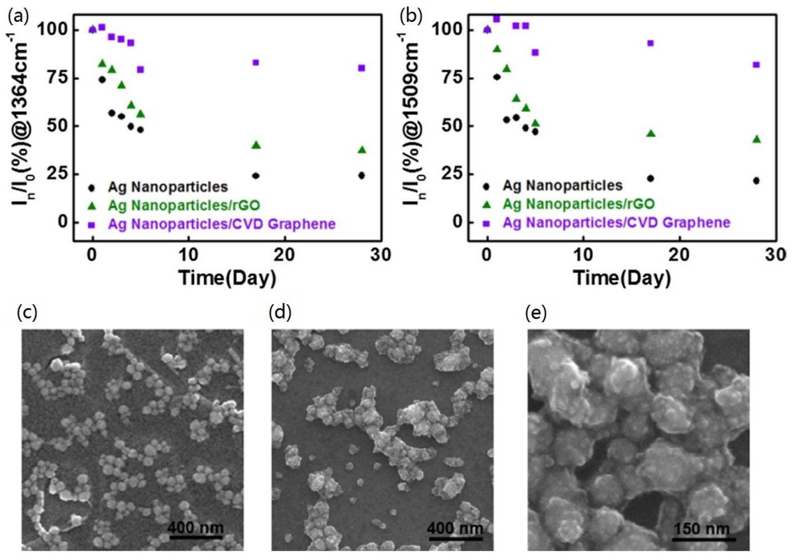
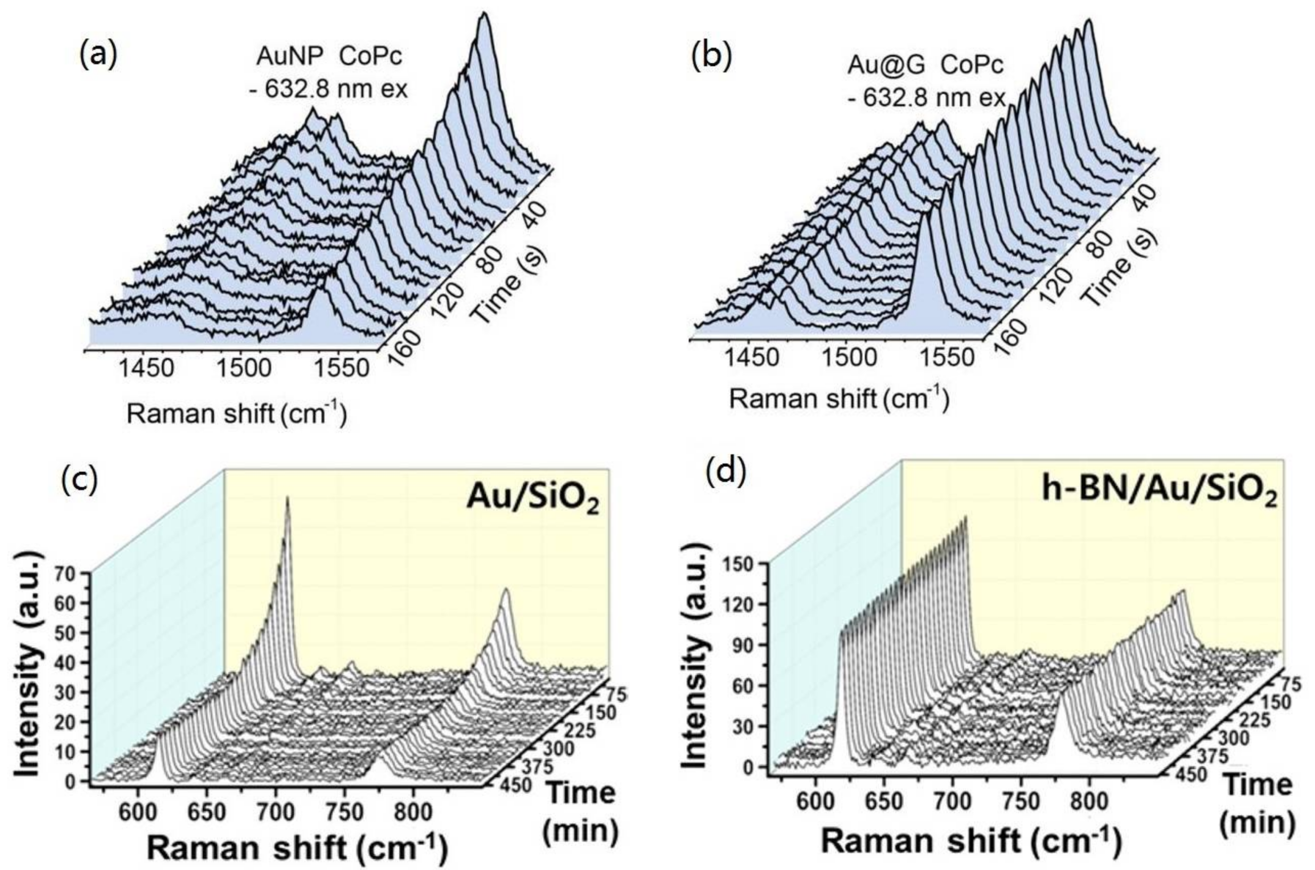
3.3. Stability
4. Conclusions and Perspective
Conflicts of Interest
References
- Pillai, I.C.; Li, S.; Romay, M.; Lam, L.; Lu, Y.; Huang, J.; Dillard, N.; Zemanova, M.; Rubbi, L.; Wang, Y. Cardiac fibroblasts adopt osteogenic fates and can be targeted to attenuate pathological heart calcification. Cell Stem Cell 2017, 20, 218–232. [Google Scholar] [CrossRef] [PubMed]
- Yigit, M.V.; Medarova, Z. In vivo and ex vivo applications of gold nanoparticles for biomedical SERS imagingi. Am. J. Nucl. Med. Mol. Imaging 2012, 2, 232–241. [Google Scholar] [PubMed]
- Qian, X.; Peng, X.-H.; Ansari, D.O.; Yin-Goen, Q.; Chen, G.Z.; Shin, D.M.; Yang, L.; Young, A.N.; Wang, M.D.; Nie, S. In vivo tumor targeting and spectroscopic detection with surface-enhanced Raman nanoparticle tags. Nat. Biotechnol. 2008, 26, 83–90. [Google Scholar] [CrossRef] [PubMed]
- Motz, J.T.; Hunter, M.; Galindo, L.H.; Gardecki, J.A.; Kramer, J.R.; Dasari, R.R.; Feld, M.S. Optical fiber probe for biomedical Raman spectroscopy. Appl. Opt. 2004, 43, 542–554. [Google Scholar] [CrossRef] [PubMed]
- Le Ru, E.C.; Etchegoin, P.G. Single-molecule surface-enhanced Raman spectroscopy. Ann. Rev. Phys. Chem. 2012, 63, 65–87. [Google Scholar] [CrossRef] [PubMed]
- Luo, S.-C.; Sivashanmugan, K.; Liao, J.-D.; Yao, C.-K.; Peng, H.-C. Nanofabricated SERS-active substrates for single-molecule to virus detection in vitro: A review. Biosens. Bioelectron. 2014, 61, 232–240. [Google Scholar] [CrossRef] [PubMed]
- Blackie, E.J.; Ru, E.C.L.; Etchegoin, P.G. Single-molecule surface-enhanced Raman spectroscopy of nonresonant molecules. J. Am. Chem. Soc. 2009, 131, 14466–14472. [Google Scholar] [CrossRef] [PubMed]
- Dasary, S.S.; Singh, A.K.; Senapati, D.; Yu, H.; Ray, P.C. Gold nanoparticle based label-free SERS probe for ultrasensitive and selective detection of trinitrotoluene. J. Am. Chem. Soc. 2009, 131, 13806–13812. [Google Scholar] [CrossRef] [PubMed]
- Lane, L.A.; Qian, X.; Nie, S. SERS nanoparticles in medicine: From label-free detection to spectroscopic tagging. Chem. Rev. 2015, 115, 10489–10529. [Google Scholar] [CrossRef] [PubMed]
- Xia, M.; Zhang, P.; Qiao, K.; Bai, Y.; Xie, Y.-H. Coupling SPP with LSPR for enhanced field confinement: A simulation study. J. Phys. Chem. C 2015, 120, 527–533. [Google Scholar] [CrossRef]
- Xia, M.; Zhang, P.; Leung, C.; Xie, Y.H. SERS optical fiber probe with plasmonic end-facet. J. Raman Spectrosc. 2017, 48, 211–216. [Google Scholar] [CrossRef]
- Xia, M.; Qiao, K.; Cheng, Z.; Xie, Y.-H. Multiple layered metallic nanostructures for strong surface-enhanced Raman spectroscopy enhancement. Appl. Phys. Express 2016, 9, 065001. [Google Scholar] [CrossRef]
- Yan, Z.; Xia, M.; Wang, P.; Zhang, P.; Liang, O.; Xie, Y.-H. Selective manipulation of molecules by electrostatic force and detection of single molecules in aqueous solution. J. Phys. Chem. C 2016, 120, 12765–12772. [Google Scholar] [CrossRef][Green Version]
- Bryche, J.-F.; Bélier, B.; Bartenlian, B.; Barbillon, G. Low-cost SERS substrates composed of hybrid nanoskittles for a highly sensitive sensing of chemical molecules. Sens. Actuators B Chem. 2017, 239, 795–799. [Google Scholar] [CrossRef]
- Jimenez de Aberasturi, D.; Serrano-Montes, A.B.; Langer, J.; Henriksen-Lacey, M.; Parak, W.J.; Liz-Marzán, L.M. Surface enhanced Raman scattering encoded gold nanostars for multiplexed cell discrimination. Chem. Mater. 2016, 28, 6779–6790. [Google Scholar] [CrossRef]
- Rodriguez-Fernandez, D.; Langer, J.; Henriksen-Lacey, M.; Liz-Marzán, L.M. Hybrid Au–SiO2 core–satellite colloids as switchable SERS tags. Chem. Mater. 2015, 27, 2540–2545. [Google Scholar] [CrossRef]
- Barbillon, G.; Sandana, V.E.; Humbert, C.; Bélier, B.; Rogers, D.J.; Teherani, F.H.; Bove, P.; McClintock, R.; Razeghi, M. Study of au coated ZnO nanoarrays for surface enhanced Raman scattering chemical sensing. J. Mater. Chem. C 2017, 5, 3528–3535. [Google Scholar] [CrossRef]
- Cui, S.; Dai, Z.; Tian, Q.; Liu, J.; Xiao, X.; Jiang, C.; Wu, W.; Roy, V.A. Wetting properties and SERS applications of ZnO/Ag nanowire arrays patterned by a screen printing method. J. Mater. Chem. C 2016, 4, 6371–6379. [Google Scholar] [CrossRef]
- Liu, L.; Yang, H.; Ren, X.; Tang, J.; Li, Y.; Zhang, X.; Cheng, Z. Au–ZnO hybrid nanoparticles exhibiting strong charge-transfer-induced SERS for recyclable SERS-active substrates. Nanoscale 2015, 7, 5147–5151. [Google Scholar] [CrossRef] [PubMed]
- Magno, G.; Bélier, B.; Barbillon, G. Gold thickness impact on the enhancement of SERS detection in low-cost Au/Si nanosensors. J. Mater. Sci. 2017, 52, 13650–13656. [Google Scholar] [CrossRef]
- Zhang, W.; Ma, R.; Chen, Q.; Xia, M.; Ng, J.; Wang, A.; Xie, Y.-H. The electro-mechanical responses of suspended graphene ribbons for electrostatic discharge applications. Appl. Phys. Lett. 2016, 108, 153103. [Google Scholar] [CrossRef]
- Chen, Q.; Ma, R.; Lu, F.; Wang, C.; Liu, M.; Wang, A.; Zhang, W.; Xia, M.; Xie, Y.-H.; Cheng, Y. Systematic transient characterization of graphene interconnects for on-chip ESD protection. In Proceedings of the 2016 IEEE International Conference on Reliability Physics Symposium (IRPS), Pasadena, CA, USA, 17–21 April 2016; pp. 3B-6-1–3B-6-5. [Google Scholar]
- Zhang, W.; Chen, Q.; Xia, M.; Ma, R.; Lu, F.; Wang, C.; Wang, A.; Xie, Y.-H. Tlp Evaluation of Esd Protection Capability of Graphene Micro-Ribbons for ICS. In Proceedings of the 2015 IEEE 11th International Conference on ASIC (ASICON), Chengdu, China, 3–6 November 2015; pp. 1–4. [Google Scholar]
- Xia, F.; Mueller, T.; Lin, Y.-M.; Valdes-Garcia, A.; Avouris, P. Ultrafast graphene photodetector. Nat. Nanotechnol. 2009, 4, 839–843. [Google Scholar] [CrossRef] [PubMed]
- Wang, X.; Wang, P.; Wang, J.; Hu, W.; Zhou, X.; Guo, N.; Huang, H.; Sun, S.; Shen, H.; Lin, T. Ultrasensitive and broadband MoS2 photodetector driven by ferroelectrics. Adv. Mater. 2015, 27, 6575–6581. [Google Scholar] [CrossRef] [PubMed]
- Ling, X.; Fang, W.; Lee, Y.-H.; Araujo, P.T.; Zhang, X.; Rodriguez-Nieva, J.F.; Lin, Y.; Zhang, J.; Kong, J.; Dresselhaus, M.S. Raman enhancement effect on two-dimensional layered materials: Graphene, h-BN and MoS2. Nano Lett. 2014, 14, 3033–3040. [Google Scholar] [CrossRef] [PubMed]
- Xu, W.; Ling, X.; Xiao, J.; Dresselhaus, M.S.; Kong, J.; Xu, H.; Liu, Z.; Zhang, J. Surface enhanced Raman spectroscopy on a flat graphene surface. Proc. Natl. Acad. Sci. 2012, 109, 9281–9286. [Google Scholar] [CrossRef] [PubMed]
- Xu, W.; Mao, N.; Zhang, J. Graphene: A platform for surface-enhanced Raman spectroscopy. Small 2013, 9, 1206–1224. [Google Scholar] [CrossRef] [PubMed]
- Wang, P.; Liang, O.; Zhang, W.; Schroeder, T.; Xie, Y.H. Ultra-sensitive graphene-plasmonic hybrid platform for label-free detection. Adv. Mater. 2013, 25, 4918–4924. [Google Scholar] [CrossRef] [PubMed]
- Wang, P.; Xia, M.; Liang, O.; Sun, K.; Cipriano, A.F.; Schroeder, T.; Liu, H.; Xie, Y.-H. Label-free SERS selective detection of dopamine and serotonin using graphene-Au nanopyramid heterostructure. Anal. Chem. 2015, 87, 10255–10261. [Google Scholar] [CrossRef] [PubMed]
- Muehlethaler, C.; Considine, C.R.; Menon, V.; Lin, W.-C.; Lee, Y.-H.; Lombardi, J.R. Ultrahigh Raman enhancement on monolayer MoS2. ACS. Photonics 2016, 3, 1164–1169. [Google Scholar] [CrossRef]
- Tan, Y.; Ma, L.; Gao, Z.; Chen, M.; Chen, F. Two-dimensional heterostructure as a platform for surface-enhanced Raman scattering. Nano Lett. 2017, 17, 2621–2626. [Google Scholar] [CrossRef] [PubMed]
- Ling, X.; Xie, L.; Fang, Y.; Xu, H.; Zhang, H.; Kong, J.; Dresselhaus, M.S.; Zhang, J.; Liu, Z. Can graphene be used as a substrate for Raman enhancement? Nano Lett. 2009, 10, 553–561. [Google Scholar] [CrossRef] [PubMed]
- Xia, M. A review on applications of two-dimensional materials in surface-enhanced Raman spectroscopy. Int. J. Spectrosc. 2018, 2018, 4861472. [Google Scholar] [CrossRef]
- Yan, Z.; Xia, M.; Zhang, P.; Xie, Y.H. Self-aligned trapping and detecting molecules using a plasmonic tweezer with an integrated electrostatic cell. Adv. Op. Mater. 2017, 5, 1600329. [Google Scholar] [CrossRef]
- Yan, Z.; Liu, Z.; Xia, M.; Efimov, A.; Xie, Y.H. Broadband surface-enhanced coherent anti-stokes Raman spectroscopy with high spectral resolution. J. Raman Spectrosc. 2017, 48, 935–942. [Google Scholar] [CrossRef]
- Ling, X.; Moura, L.; Pimenta, M.A.; Zhang, J. Charge-transfer mechanism in graphene-enhanced Raman scattering. J. Phys. Chem. C 2012, 116, 25112–25118. [Google Scholar] [CrossRef]
- Ling, X.; Zhang, J. First-layer effect in graphene-enhanced Raman scattering. Small 2010, 6, 2020–2025. [Google Scholar] [CrossRef] [PubMed]
- Liang, E.; Kiefer, W. Chemical effect of SERS with near-infrared excitation. J. Raman Spectrosc. 1996, 27, 879–886. [Google Scholar] [CrossRef]
- Kneipp, K.; Wang, Y.; Kneipp, H.; Perelman, L.T.; Itzkan, I.; Dasari, R.R.; Feld, M.S. Single molecule detection using surface-enhanced Raman scattering (SERS). Phys. Rev. Lett. 1997, 78, 1667. [Google Scholar] [CrossRef]
- Xu, H.; Aizpurua, J.; Käll, M.; Apell, P. Electromagnetic contributions to single-molecule sensitivity in surface-enhanced Raman scattering. Phys. Rev. E 2000, 62, 4318. [Google Scholar] [CrossRef]
- Le Ru, E.C.; Etchegoin, P.G. Principles of Surface-Enhanced Raman Spectroscopy: And Related Plasmonic Effects; Elsevier: New York, NY, USA, 2008. [Google Scholar]
- Moskovits, M. Surface-enhanced spectroscopy. Rev. Mod. Phys. 1985, 57, 783. [Google Scholar] [CrossRef]
- Adrian, F.J. Charge transfer effects in surface-enhanced Raman scatteringa. J. Chem. Phys. 1982, 77, 5302–5314. [Google Scholar] [CrossRef]
- Ling, X.; Wu, J.; Xu, W.; Zhang, J. Probing the effect of molecular orientation on the intensity of chemical enhancement using graphene-enhanced Raman spectroscopy. Small 2012, 8, 1365–1372. [Google Scholar] [CrossRef] [PubMed]
- Dean, C.R.; Young, A.F.; Meric, I.; Lee, C.; Wang, L.; Sorgenfrei, S.; Watanabe, K.; Taniguchi, T.; Kim, P.; Shepard, K.L. Boron nitride substrates for high-quality graphene electronics. Nat. Nanotechnol. 2010, 5, 722. [Google Scholar] [CrossRef] [PubMed]
- Splendiani, A.; Sun, L.; Zhang, Y.; Li, T.; Kim, J.; Chim, C.-Y.; Galli, G.; Wang, F. Emerging photoluminescence in monolayer MoS2. Nano Lett. 2010, 10, 1271–1275. [Google Scholar] [CrossRef] [PubMed]
- Liu, Y.; Yu, D.; Zeng, C.; Miao, Z.; Dai, L. Biocompatible graphene oxide-based glucose biosensors. Langmuir 2010, 26, 6158–6160. [Google Scholar] [CrossRef] [PubMed]
- Li, N.; Zhang, Q.; Gao, S.; Song, Q.; Huang, R.; Wang, L.; Liu, L.; Dai, J.; Tang, M.; Cheng, G. Three-dimensional graphene foam as a biocompatible and conductive scaffold for neural stem cells. Sci. Rep. 2013, 3, 1604. [Google Scholar] [CrossRef] [PubMed]
- Weng, Q.; Wang, B.; Wang, X.; Hanagata, N.; Li, X.; Liu, D.; Wang, X.; Jiang, X.; Bando, Y.; Golberg, D. Highly water-soluble, porous, and biocompatible boron nitrides for anticancer drug delivery. ACS Nano 2014, 8, 6123–6130. [Google Scholar] [CrossRef] [PubMed]
- Zhu, Y.; Murali, S.; Cai, W.; Li, X.; Suk, J.W.; Potts, J.R.; Ruoff, R.S. Graphene and graphene oxide: Synthesis, properties, and applications. Adv. Mater. 2010, 22, 3906–3924. [Google Scholar] [CrossRef] [PubMed]
- Li, X.; Zhu, H. Two-dimensional MoS2: Properties, preparation, and applications. J. Mater. 2015, 1, 33–44. [Google Scholar] [CrossRef]
- Zhang, K.; Feng, Y.; Wang, F.; Yang, Z.; Wang, J. Two dimensional hexagonal boron nitride (2D-hBN): Synthesis, properties and applications. J. Mater. Chem. C 2017, 5, 11992–12022. [Google Scholar] [CrossRef]
- Fan, M.; Andrade, G.F.; Brolo, A.G. A review on the fabrication of substrates for surface enhanced Raman spectroscopy and their applications in analytical chemistry. Anal. Chim. Acta 2011, 693, 7–25. [Google Scholar] [CrossRef] [PubMed]
- Brown, R.J.; Milton, M.J. Nanostructures and nanostructured substrates for surface—Enhanced Raman scattering (SERS). J. Raman Spectrosc. 2008, 39, 1313–1326. [Google Scholar] [CrossRef]
- Ouyang, L.; Ren, W.; Zhu, L.; Irudayaraj, J. Prosperity to challenges: Recent approaches in SERS substrate fabrication. Rev. Anal. Chem. 2017, 36, 20160027. [Google Scholar] [CrossRef]
- Xia, M.; Li, B.; Yin, K.; Capellini, G.; Niu, G.; Gong, Y.; Zhou, W.; Ajayan, P.M.; Xie, Y.-H. Spectroscopic signatures of AA′ and AB stacking of chemical vapor deposited bilayer MoS2. ACS Nano 2015, 9, 12246–12254. [Google Scholar] [CrossRef] [PubMed]
- Zhu, X.; Shi, L.; Schmidt, M.S.; Boisen, A.; Hansen, O.; Zi, J.; Xiao, S.; Mortensen, N.A. Enhanced light–matter interactions in graphene-covered gold nanovoid arrays. Nano Lett. 2013, 13, 4690–4696. [Google Scholar] [CrossRef] [PubMed]
- Li, H.; Contryman, A.W.; Qian, X.; Ardakani, S.M.; Gong, Y.; Wang, X.; Weisse, J.M.; Lee, C.H.; Zhao, J.; Ajayan, P.M. Optoelectronic crystal of artificial atoms in strain-textured molybdenum disulphide. Nat. Commun. 2015, 6, 7381. [Google Scholar] [CrossRef] [PubMed]
- Pirkle, A.; Chan, J.; Venugopal, A.; Hinojos, D.; Magnuson, C.; McDonnell, S.; Colombo, L.; Vogel, E.; Ruoff, R.; Wallace, R. The effect of chemical residues on the physical and electrical properties of chemical vapor deposited graphene transferred to SiO2. Appl. Phys. Lett. 2011, 99, 122108. [Google Scholar] [CrossRef]
- Kim, Y.-K.; Han, S.W.; Min, D.-H. Graphene oxide sheath on Ag nanoparticle/graphene hybrid films as an antioxidative coating and enhancer of surface-enhanced Raman scattering. ACS Appl. Mater. Interfaces 2012, 4, 6545–6551. [Google Scholar] [CrossRef] [PubMed]
- Hu, Y.; Li, F.; Bai, X.; Li, D.; Hua, S.; Wang, K.; Niu, L. Label-free electrochemical impedance sensing of DNA hybridization based on functionalized graphene sheets. Chem. Commun. 2011, 47, 1743–1745. [Google Scholar] [CrossRef] [PubMed]
- Georgakilas, V.; Otyepka, M.; Bourlinos, A.B.; Chandra, V.; Kim, N.; Kemp, K.C.; Hobza, P.; Zboril, R.; Kim, K.S. Functionalization of graphene: Covalent and non-covalent approaches, derivatives and applications. Chem. Rev. 2012, 112, 6156–6214. [Google Scholar] [CrossRef] [PubMed]
- Shan, C.; Yang, H.; Han, D.; Zhang, Q.; Ivaska, A.; Niu, L. Water-soluble graphene covalently functionalized by biocompatible poly-l-lysine. Langmuir 2009, 25, 12030–12033. [Google Scholar] [CrossRef] [PubMed]
- Liu, Y.; Hu, Y.; Zhang, J. Few-layer graphene-encapsulated metal nanoparticles for surface-enhanced Raman spectroscopy. J. Phys. Chem. C 2014, 118, 8993–8998. [Google Scholar] [CrossRef]
- Wei, D.; Lu, Y.; Han, C.; Niu, T.; Chen, W.; Wee, A.T.S. Critical crystal growth of graphene on dielectric substrates at low temperature for electronic devices. Angew. Chem. Int. Ed. 2013, 52, 14121–14126. [Google Scholar] [CrossRef] [PubMed]
- Qi, J.; Zheng, W.; Zheng, X.; Wang, X.; Tian, H. Relatively low temperature synthesis of graphene by radio frequency plasma enhanced chemical vapor deposition. Appl. Surf. Sci. 2011, 257, 6531–6534. [Google Scholar] [CrossRef]
- Sun, J.; Chen, Y.; Cai, X.; Ma, B.; Chen, Z.; Priydarshi, M.K.; Chen, K.; Gao, T.; Song, X.; Ji, Q. Direct low-temperature synthesis of graphene on various glasses by plasma-enhanced chemical vapor deposition for versatile, cost-effective electrodes. Nano Res. 2015, 8, 3496–3504. [Google Scholar] [CrossRef]
- Scarabelli, L.; Coronado-Puchau, M.; Giner-Casares, J.J.; Langer, J.; Liz-Marzán, L.M. Monodisperse gold nanotriangles: Size control, large-scale self-assembly, and performance in surface-enhanced Raman scattering. ACS Nano 2014, 8, 5833–5842. [Google Scholar] [CrossRef] [PubMed]
- McLellan, J.M.; Li, Z.-Y.; Siekkinen, A.R.; Xia, Y. The SERS activity of a supported Ag nanocube strongly depends on its orientation relative to laser polarization. Nano Lett. 2007, 7, 1013–1017. [Google Scholar] [CrossRef] [PubMed]
- Nie, S.; Emory, S.R. Probing single molecules and single nanoparticles by surface-enhanced Raman scattering. Science 1997, 275, 1102–1106. [Google Scholar] [CrossRef] [PubMed]
- Kha, N.M.; Chen, C.-H.; Su, W.-N.; Rick, J.; Hwang, B.-J. Improved Raman and photoluminescence sensitivity achieved using bifunctional Ag@SiO2 nanocubes. Phys. Chem. Chem. Phys. 2015, 17, 21226–21235. [Google Scholar] [CrossRef] [PubMed]
- Sakano, T.; Tanaka, Y.; Nishimura, R.; Nedyalkov, N.N.; Atanasov, P.A.; Saiki, T.; Obara, M. Surface enhanced raman scattering properties using Au-coated ZnO nanorods grown by two-step, off-axis pulsed laser deposition. J. Phys. D Appl. Phys. 2008, 41, 235304. [Google Scholar] [CrossRef]
- Kim, G.; Kim, M.; Hyun, C.; Hong, S.; Ma, K.Y.; Shin, H.S.; Lim, H. Hexagonal boron nitride/au substrate for manipulating surface plasmon and enhancing capability of surface-enhanced Raman spectroscopy. ACS Nano 2016, 10, 11156–11162. [Google Scholar] [CrossRef] [PubMed]
- Liu, Z.; Gong, Y.; Zhou, W.; Ma, L.; Yu, J.; Idrobo, J.C.; Jung, J.; MacDonald, A.H.; Vajtai, R.; Lou, J. Ultrathin high-temperature oxidation-resistant coatings of hexagonal boron nitride. Nat. Commun. 2013, 4, 2541. [Google Scholar] [CrossRef] [PubMed]
- Chen, S.; Brown, L.; Levendorf, M.; Cai, W.; Ju, S.-Y.; Edgeworth, J.; Li, X.; Magnuson, C.W.; Velamakanni, A.; Piner, R.D. Oxidation resistance of graphene-coated Cu and Cu/Ni alloy. ACS Nano 2011, 5, 1321–1327. [Google Scholar] [CrossRef] [PubMed]
- Liu, X.; Wang, J.; Wu, Y.; Fan, T.; Xu, Y.; Tang, L.; Ying, Y. Compact shielding of graphene monolayer leads to extraordinary SERS-active substrate with large-area uniformity and long-term stability. Sci. Rep. 2015, 5, 17167. [Google Scholar] [CrossRef] [PubMed]
- Hu, Y.; Kumar, P.; Xuan, Y.; Deng, B.; Qi, M.; Cheng, G.J. Controlled and stabilized light–matter interaction in graphene: Plasmonic film with large-scale 10-nm lithography. Adv. Opt. Mater. 2016, 4, 1811–1823. [Google Scholar] [CrossRef]
- Li, X.; Li, J.; Zhou, X.; Ma, Y.; Zheng, Z.; Duan, X.; Qu, Y. Silver nanoparticles protected by monolayer graphene as a stabilized substrate for surface enhanced Raman spectroscopy. Carbon 2014, 66, 713–719. [Google Scholar] [CrossRef]
- Du, Y.; Zhao, Y.; Qu, Y.; Chen, C.-H.; Chen, C.-M.; Chuang, C.-H.; Zhu, Y. Enhanced light–matter interaction of graphene–gold nanoparticle hybrid films for high-performance SERS detection. J. Mater. Chem. C 2014, 2, 4683–4691. [Google Scholar] [CrossRef]
- Zhao, Y.; Xie, Y.; Bao, Z.; Tsang, Y.H.; Xie, L.; Chai, Y. Enhanced SERS stability of R6G molecules with monolayer graphene. J. Phys. Chem. C 2014, 118, 11827–11832. [Google Scholar] [CrossRef]
- Xie, L.; Ling, X.; Fang, Y.; Zhang, J.; Liu, Z. Graphene as a substrate to suppress fluorescence in resonance Raman spectroscopy. J. Am. Chem. Soc. 2009, 131, 9890–9891. [Google Scholar] [CrossRef] [PubMed]


| SERS Substrate Type | Substrate Materials | Enhancement Factor | Analytes | Ref. |
|---|---|---|---|---|
| Metal | Au nanotriangles | 1.2 × 10⁵ | Benzenethiol | [69] |
| Ag nanocubes | 1.25 × 10⁵ | 1,4-benzenedithiol | [70] | |
| Ag nanoparticles | 1014–1015 | Rhodamine 6G | [71] | |
| Metal/inorganic hybrid structure | SiO2-coated silver nanocubes | 1.2 × 10⁶ | Rhodamine 6G | [72] |
| Au nanoparticle-coated ZnO nanoneedles | 1.2 × 10⁷ | Rhodamine 6G | [19] | |
| Au-coated ZnO nanorods | 106 | Rhodamine 6G | [73] | |
| 2D materials/Metal hybrid structure | Monolayer graphene-coated Au nanopyramids | 1010 | Rhodamine 6G and lysozyme | [29] |
| Monolayer graphene-coated Au nanovoids | 103 | Rhodamine 6G | [58] | |
| Few layer graphene-coated Au nanoparticles | 9.2–19.4 | Cobalt phthalocyanine | [65] | |
| 2D materials | Monolayer graphene | 2–17 | Phthalocyanine | [33] |
| Monolayer MoS2 | 5 × 10⁴–3.8 × 10⁵ | 4-mercaptopyridine | [31] | |
| h-BN | 6.9–41 | Copper phthalocyanine | [26] | |
| Monolayer WSe2 | 0.18–4.7 | Copper phthalocyanine | [32] | |
| Monolayer graphene on top of monolayer WS2 | 3.8–78.2 | Copper phthalocyanine | [32] |
| SERS Peaks (cm−1) | Peak Assignment | Average Enhancement (IGraphene/Au tip/IAu tip) |
|---|---|---|
| 613 | δ(C–C–C)ip | 10 |
| 775 | δ(C–H)op | 5 |
| 1187 | δ(C–H)ip | 2 |
| 1311 | ν(C–C)+, ν(C–N) | 6 |
| 1360 | ν(C–C)+, ν(C–N) | 6 |
| 1506 | ν(C–C) | 4 |
| 1577 | ν(C–O–C) | 8 |
© 2018 by the author. Licensee MDPI, Basel, Switzerland. This article is an open access article distributed under the terms and conditions of the Creative Commons Attribution (CC BY) license (http://creativecommons.org/licenses/by/4.0/).
Share and Cite
Xia, M. 2D Materials-Coated Plasmonic Structures for SERS Applications. Coatings 2018, 8, 137. https://doi.org/10.3390/coatings8040137
Xia M. 2D Materials-Coated Plasmonic Structures for SERS Applications. Coatings. 2018; 8(4):137. https://doi.org/10.3390/coatings8040137
Chicago/Turabian StyleXia, Ming. 2018. "2D Materials-Coated Plasmonic Structures for SERS Applications" Coatings 8, no. 4: 137. https://doi.org/10.3390/coatings8040137
APA StyleXia, M. (2018). 2D Materials-Coated Plasmonic Structures for SERS Applications. Coatings, 8(4), 137. https://doi.org/10.3390/coatings8040137