Article

Conductive Characteristics of Indium Tin Oxide Thin Film on Polymeric Substrate under Long-Term Static Deformation

Department of Mechanical Engineering, National Central University, Jhong-Li District, Tao-Yuan 32001, Taiwan
*
Author to whom correspondence should be addressed.
Coatings 2018, 8(6), 212; https://doi.org/10.3390/coatings8060212
Submission received: 17 April 2018 / Revised: 25 May 2018 / Accepted: 29 May 2018 / Published: 1 June 2018

Abstract

:
The objective of this study is to investigate the effect of long-term static bending on the conductive characteristics of indium tin oxide (ITO) thin film in flexible optoelectronics. Two types of substrate are considered, namely ITO on polyethylene naphthalate (ITO/PEN) and ITO on polyethylene terephthalate (ITO/PET). Electrical properties of the ITO/PEN and ITO/PET sheets are measured in situ under static bending at various radii of curvature. Experimental results indicate that no significant change in electrical resistance of the ITO/PEN and ITO/PET sheets is found for compressive bending after 1000 h at a curvature radius of 10 mm or larger. However, the ITO/PEN and ITO/PET sheets are seriously damaged under a tensile bending of 10 mm radius and 5 mm radius, respectively. The given ITO/PET sheet exhibits a greater resistance to long-term mechanical bending than the ITO/PEN one, which is attributed to the effect of stiffness and thickness of substrate. As the given PET substrate has a lower stiffness and thickness than the PEN one, ITO thin film in the ITO/PET sheet has a smaller stress given a bending radius. Consequently, a smaller extent of change in the electrical conductance of ITO thin film is found in the ITO/PET sheet.

1. Introduction

Flexible organic optoelectronics has recently received much attention due to several advantages, such as flexibility, impact resistance, light weight, low cost, and possible roll-to-roll mass production. It is a promising subject for continuous investigation and development. Organic materials are commonly used as semiconductor components in flexible optoelectronics, thanks to their extremely flexible and ductile properties. Applications of organic semiconductor components in flexible electronics include organic light emitting diode (OLED), organic photovoltaic (OPV), and organic thin film transistor (OTFT) [1]. Flexible optoelectronics are expected to create more innovative applications in the future. In order to make highly efficient organic semiconductor components, transparent conductive layers are needed. The most common transparent conductive layers for flat panel displays, electroluminescent and electrochromic displays, OPV, and OLED are indium tin oxide (ITO) thin films [2]. They can be deposited by various techniques such as magnetron sputtering, reactive evaporation, radio frequency sputtering, spray pyrolysis, pulsed laser deposition, and screen printing process [3,4,5]. Manufacturing of ITO thin films needs precious raw materials and expensive tools, which limits their compatibility with mass production and low-cost devices [3]. Although alternatives for transparent conductive film are available, such as zinc-doped indium oxide, gallium-doped zinc oxide, and aluminum-doped zinc oxide [4], due to its excellent electrical characteristics and high transparency, ITO is still the best candidate for the organic semiconductor components at present [6,7,8,9,10,11]. However, the natural brittle characteristic of ITO thin film results in damage after mechanical bending, and causes challenges for implementation in flexible organic optoelectronics. Therefore, its bending behavior needs to be studied for better applications in flexible optoelectronics.
The most common chemical compositions considered for polymer substrate in flexible organic optoelectronics are polyethylene terephthalate (PET), polyethylene naphthalate (PEN), and polyethersulfone (PES). A material with a greater Young’s modulus is usually more brittle than a low one. Note that PET has a smaller Young’s modulus, such that it has better flexibility [12,13,14]. On the other hand, heat-resistance also needs to be considered in the roll-to-roll fabrication process of flexible electronics. PET has the lowest glass transition temperature (Tg) among the aforementioned three materials, while PES has the highest one [12,13,14]. Therefore, PES is more suitable for high-temperature manufacturing processes. The material properties of PEN are in-between, and it is also considered as a favorite substrate for flexible optoelectronics. In this study, PET and PEN are selected to study the substrate effect on the bending performance of ITO thin film.
Currently, many studies have been conducted to find ways to improve conductive property and/or mechanical performance or to investigate failure mechanism of ITO thin film under bending [7,12,15,16,17,18,19,20,21,22,23,24,25,26,27,28,29,30,31,32,33,34,35,36,37,38,39,40,41,42]. Lim et al. [12] studied the flexural ability of ITO on PES, PET, and PEN substrates at different radii of curvature under cyclic bending [12]. Their results show that Young’s modulus of the substrate significantly affects the conductive stability of ITO electrode and mechanical properties of ITO/substrate film [12]. A cyclic bending test was also conducted to investigate the electrical conductivity of ITO thin film under various conditions of temperature and humidity [20,42]. Their results show that cyclic bending deformation is the dominant factor for the electrical resistance increase in those ITO films. That cyclic bending method was also applied to addressing the failure behavior of aluminum-doped zinc oxide thin film in harshly environmental conditions [43,44,45,46]. In addition to cyclic bending test, Hamasha et al. also investigated the conductivity behavior of ITO film under various stretching rates [47]. A three-point bending test combined with dynamic stiffness measurement was used to study deformation change and brittle failure mechanism of ITO thin film by Kirubanandham and Basu [15]. Their results show that bending causes buckling, delamination, and cracking in ITO thin film, and leads to an electrical resistance rise [15]. Lim et al. [38] studied the bending reliability of an ITO thin film on a 125 μm-thick PET substrate, by decreasing the bending radius, to define the critical bending radius. Electrical resistance of that ITO thin film was synchronously measured as the bending radius continued to decrease from 40 mm to 3 mm [38]. Their results show that the critical bending radii of 20, 50, 100, and 150 nm-thick ITO electrodes are 4.5, 4.5, 6, and 6 mm, respectively [38]. Leppänen et al. [40] investigated the mechanical and electrical behavior of an ITO thin film under static bending at different curvatures. Samples were bent from 53 mm to 15 mm radius of curvature [40]. Electrical resistance measurement and cracking observation were immediately conducted after 0, 2, and 24 h of bending [40]. The results show that cracks appear at 20 mm-radius cylinder and smaller, in conjunction with slight degradation in the conductivity of ITO thin film [40]. The exemplified results, described above, indicate that the electrical performance of ITO films is degraded under certain bending conditions.
As flexible optoelectronic devices can be curved like paper in applications, the most attractive feature is their flexibility. For prolonged use of such devices, long-term failure mechanisms related to electrical characteristics of conductive layers of flexible organic optoelectronics should be considered. Although investigations on electrical conductivity of ITO thin films under bending have been conducted in previous studies, the change of electrical conductivity is mostly assessed after cyclic bending [12,15,16,17,20,22,31,42,48,49,50,51] or static bending [40]. However, it is necessary to study the concurrent change of electrical conductivity of ITO thin film under long-term mechanical bending, and its correlation with the mechanical failure mechanism. In our prior work [41], the effect of cyclic bending on the in situ variation of electrical conductance of ITO thin film has been investigated. In this study, changes of electrical conductance in ITO thin film on different polymer substrates are investigated by conducting long-term static bending tests with various radii of curvature. Particularly, electrical conductivity of the given ITO thin films is monitored by in situ electrical resistance measurement during static bending up to 1000 h. Hopefully, such results could help assess lifetime of flexible optoelectronics and clarify the relevant failure mechanisms for long-term static bending.

2. Experimental Procedures

2.1. Materials and Specimen Preparation

Two types of ITO thin film are investigated, one using PET as the substrate and the other using PEN. The ITO thin film on PET substrate (ITO/PET) sheets were purchased from Win-Optical Technology Co., Ltd., (Tao-Yuan, Taiwan). According to product specifications [52], surface resistance of the ITO thin film is 150 Ω/sq after annealing at 150 °C for 90 min. The ITO/PET sheets were received in a form of A4 sheets with a thickness of 133 μm. Rectangular samples in physical dimensions of 36, 51, 83, 114, and 145 mm (length) × 10 mm (width) are cut out to conduct static bending tests at various radii of curvature, namely 5, 10, 20, 30, and 40 mm, respectively. The ITO thin film on PEN substrate (ITO/PEN) sheets were fabricated by Peccell Technologies, Inc., (Yokohama, Japan) and purchased through Ruilong Co., Ltd., (Miao-Li, Taiwan). According to product specifications [13], its surface resistance is less than 15 Ω/sq. The as-fabricated ITO/PEN sheets were received in a form of 20 cm × 25 cm × 200 μm [13]. Rectangular samples are cut out of the ITO/PEN sheets for static bending tests and have the same dimensions of the ITO/PET samples.

2.2. Static Bending Test

For investigating the effect of long-term static bending on electrical conductance of the given ITO thin films, a fixture of static bending test is designed and made in-house, as shown in Figure 1. Each ITO thin film sample is firstly clamped by two stainless steel clips at both ends, as shown in Figure 1. The two clips are then fixed on a flat plate. As the sample is bent in a concave downward position (Figure 1), ITO thin layer is under tension when placed at the top position. ITO thin layer is subjected to compressive stress when it is placed at the bottom of the sample. Five radii of curvature (5, 10, 20, 30, and 40 mm) are applied for static bending tests, and the specimens are continuously bent until 1000 h. During the bending test, all the specimens are placed in a closed box at room temperature to avoid dust accumulating on the specimens.
During the static bending test, the electrical resistance of ITO film is monitored using a source measurement unit (SMU-Keithley 2400, Keithley Instruments, Inc., Cleveland, OH, USA). For measuring electrical resistance of several ITO film samples at the same time, the source measurement unit is combined with a homemade switch system controlled by a LabVIEW program, as shown in Figure 2. This homemade switch system, which consists of a relay module and a microcontroller (Arduino Mega 2560, Arduino LLC, Turin, Piedmont, Italy), is in contact with an array of eight ITO specimens through electrical wires. The electrical wires and relay contacts are used as electrical current entrances to measure the electrical resistance, thanks to their high conductivity and negligible resistance. During the measurement, the electrical current is continuously recorded by the given source measurement unit under a constant source voltage of 20 mV. The resistance change of each ITO sample is then in situ determined throughout the bending test.

2.3. Microstructural Analysis

In order to determine coating thickness of the ITO thin films studied, some specimens are cut along the thickness direction to observe the cross-sectional microstructure using a scanning electron microscope (SEM) (Hitachi S-800, Hitachi, Ltd., Tokyo, Japan). Pt films are deposited on the specimens to prevent accumulation of electrostatic charge at the surface. After mechanical bending test, fracture surfaces of the ITO/PET and ITO/PEN specimens are observed using an optical microscope (OM) and SEM to analyze the failure mechanism. In addition, the surface morphology and roughness profiles of ITO/PEN and ITO/PET sheets in as-received and after-bending states are characterized by atomic force microscopy (AFM) (XE 7, Park Systems, Suwon, Korea). The microstructural changes, interfacial cracks, and bonding defects observed are correlated with the electrical resistance change of the mechanically bent ITO/PET and ITO/PEN samples.

3. Results and Discussion

3.1. Bending Effect on ITO Thin Film

The electrical resistance change of ITO/PEN and ITO/PET sheets with time under static bending at various radii of curvature are shown in Figure 3 and Figure 4, respectively. Two specimens are repeatedly tested for a given bending condition to check the repeatability of data. In addition, each figure shows the results of four samples bent at a similar radius of curvature, namely two under tension (Tensile 1 and 2) and the other two under compression (Compressive 1 and 2). Note that in Figure 3 and Figure 4, change of the resistance is normalized by its original value and plotted in the ordinate. As shown in Figure 3 and Figure 4, a slight reduction of electrical resistance of ITO thin film is generally observed at the beginning of compressive bending for both ITO/PEN and ITO/PET sheets. The initial reduction of electrical resistance under compressive bending for ITO/PEN sheet is about 20% and 2% at a 10 mm and a 20 mm curvature radius, respectively. For ITO/PET sheet, the initial reduction under compressive bending is about 50%, 7%, and 1% at a radius of 5 mm, 10 mm, and 20 mm, respectively. For a change from neutral state to compressive state, a reduction of electrical resistivity occurs because of a net decrement in the space between ITO aggregates, which produces more conduction paths [53,54]. When the ITO/PET sheet is bent in tension, a slight reduction of electrical resistance is also observed at the beginning for bending radius of 10 mm or 20 mm. The extent of initial reduction is about 6% and 1% for the 10 mm and 20 mm curvature radius, respectively. This is attributable to the fact that a rotation of ITO aggregates may cause additional connections of ITO aggregates in response to the longitudinal expansion of specimen under tension. This phenomenon is called an orientation effect of non-uniformly spaced aggregates of nanostructured substance [53]. A lower electrical resistance in a compressive or tensile state than that in a neutral state is also observed for the given ITO thin films under cyclic bending in our previous study [41].
As shown in Figure 3a, the electrical resistance changes of ITO/PEN under both tensile and compressive bending with a 40 mm curvature radius are about 2% after 1000 h of static bending. The electrical resistance change under 1000 h of tensile or compressive bending with a 30 mm curvature radius is also about 2% (Figure 3b). No significantly detrimental effect on the electrical conductance of ITO/PEN sheet is found for bending with a radius of curvature of 30 mm or 40 mm. As shown in Figure 3c, the electrical resistance change gradually increases with time under both tensile and compressive bending with a 20 mm curvature radius. Compared with the initial reduction of electrical resistance at beginning of bending, the electrical resistance changes after 1000 h of tensile and compressive bending are about 3–5% and 3%, respectively. The electrical resistance of ITO/PEN significantly increases with time under tensile bending with a 10 mm curvature radius, and a change of 800–900% is found after 1000 h of bending (Figure 3d). However, for a similar bending radius of 10 mm, the electrical resistance of ITO/PEN only increases by 3% after 1000 h of compressive bending.
An overall comparison of the results presented in Figure 3 indicates that a detrimental tensile bending effect is found for a curvature of 20 mm and smaller. In particular, as the bending radius is decreased to 10 mm, the electrical resistance significantly increases to an extent of about 500% at the beginning, and 800–900% after 1000 h. On the other hand, a slight effect of compressive bending is found for bending radius of 20 mm and smaller. The electrical resistance slightly decreases by 2% at the beginning, and increases by 3% after 1000 h of bending with a radius of 20 mm. When the bending radius is reduced to 10 mm for more severe bending, no further detrimental effect is observed, and the electrical resistance change is similar to that of 20 mm. These results reveal that tensile bending is much more detrimental than compressive bending to the electrical conductance of the given ITO/PEN sheet under a long-term static flexural deformation.
As shown in Figure 4a,b, the electrical resistance changes of ITO/PET under both tensile and compressive bending with 30 mm and 20 mm curvature radii are about 2% after 1000 h of bending. Therefore, no significantly detrimental effect on the electrical conductance of ITO/PET sheet is found for a bending radius of 20 mm or 30 mm. As shown in Figure 4c, the electrical resistance change under tensile bending with a 10 mm curvature radius starts to increase at 100 h, and reaches a change of 6–20% at 1000 h. For a bending radius of 5 mm, the electrical resistance significantly increases from the beginning of tensile bending, and has a change of 60,000% after 1000 h (Figure 4d). However, for a compressive bending state with a radius of curvature of 10 mm or 5 mm, no significant change of electrical resistance is found, as shown in Figure 4c,d. As the ITO/PET sheet is seriously damaged at the beginning of tensile bending with a 5 mm curvature radius in a repeated test, no long-term static bending is conducted on this repeated sample.
Comparison of the electrical resistance changes of ITO/PET sheet presented in Figure 4 indicates that a detrimental tensile bending effect is found for curvature radius of 10 mm and smaller. In particular, for a bending radius of 5 mm, tensile bending increases, extremely, the electrical resistance to an extent of 50,000% at beginning, and 60,000% after 1000 h of bending. Such a great change of electrical resistance makes the damaged ITO/PET sheet almost nonconductive. On the contrary, the electrical conductance of the ITO/PET sheet remains stable for all the compressive states of long-term static bending. This indicates, again, that tensile bending is much more detrimental than compressive bending to the electrical conductance of the given ITO/PET sheet under a long-term static flexural deformation.
In comparison of ITO/PEN and ITO/PET sheets under tensile bending (Figure 3 and Figure 4), electrical resistance of the ITO/PEN sheet slightly increases at a bending radius of 20 mm, but the ITO/PET sheet remains stable up to 1000 h. When the bending radius is reduced to 10 mm for more severe bending, electrical resistance of the ITO/PEN sheet significantly increases, but electrical resistance of the ITO/PET sheet just slightly increases. For a counterpart comparison under compressive bending, these two ITO sheets show no significant change in electrical resistance at a bending radius of 30 mm or larger. For more severe bending of 20 mm and 10 mm radii, electrical resistance of the ITO/PET sheet is still stable under compressive bending after 1000 h, but electrical resistance of the ITO/PEN sheet slightly increases. Based on the comparisons described above, the given ITO/PET sheet exhibits a greater resistance to long-term static bending than the ITO/PEN sheet in terms of change in electrical conductance.

3.2. Failure Analysis

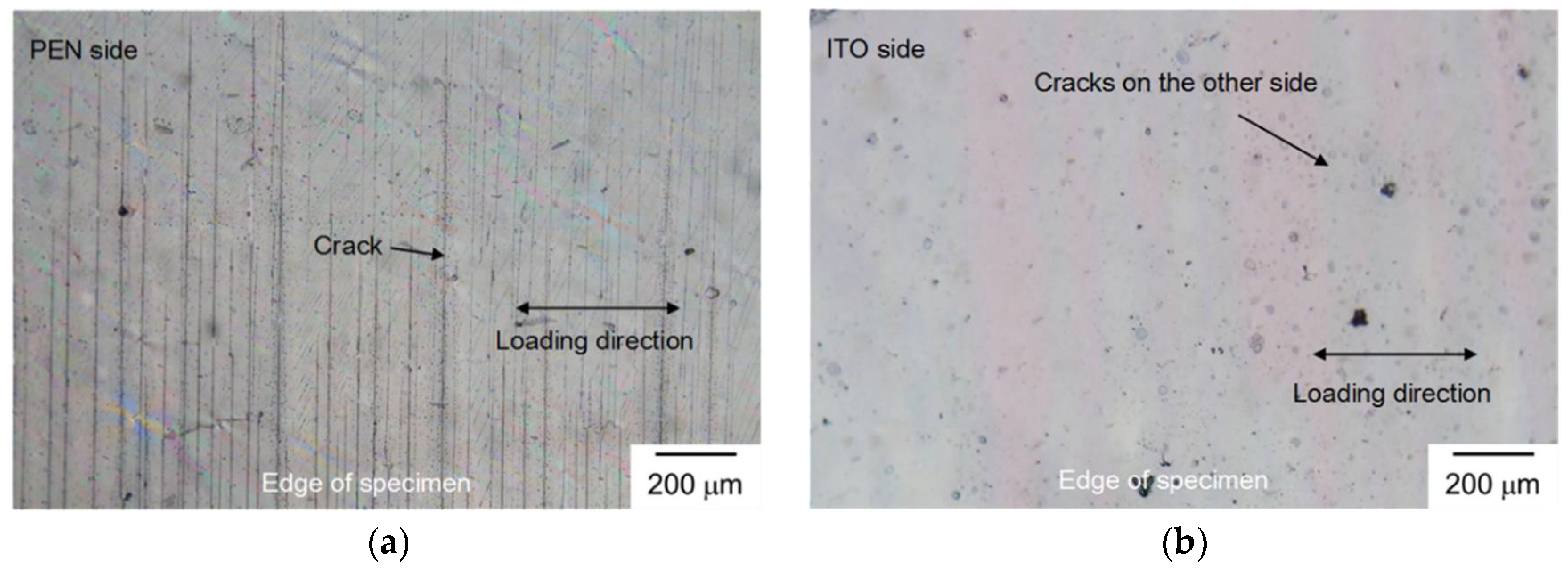
As described in Section 3.1, given a bending radius of 10 mm, the electrical resistance of ITO/PEN sheet increases significantly by 800–900% under tensile bending, and increases only by 3% under compressive bending after 1000 h. OM micrographs of ITO/PEN sheet after 1000 h of compressive and tensile bending with a 10 mm curvature radius are shown in Figure 5 and Figure 6, respectively. Cracks are found in both specimens, and are presumably initiated at the edge of the specimen, as shown in Figure 5 and Figure 6. However, cracks develop on the PEN substrate when ITO is under compressive bending, and on the ITO thin film when ITO is under tensile bending, as shown in Figure 5a and Figure 6b, respectively. As shown in Figure 6b, wrinkles are also found in the ITO/PEN sheet after tensile bending. Existence of wrinkles is attributed to shrinkage deformation caused by Poisson’s effect in the underlying film [55]. As deformability of the underlying film is much higher than that of the ITO film, part of the ITO film is wrinkled up [55]. These results reveal that static bending of 10 mm radius seriously damages the ITO/PEN sheet in both compressive and tensile states, but the ITO thin film is damaged only under tensile bending.
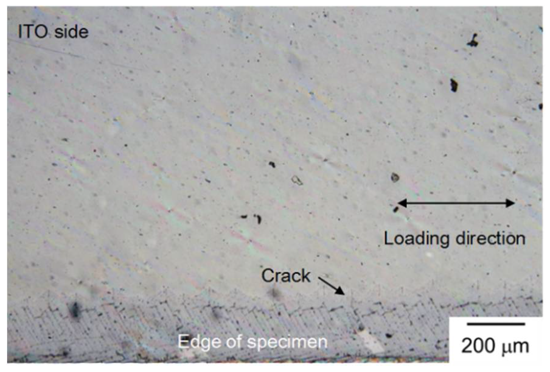
For a larger bending radius of 20 mm, the electrical resistance of ITO/PEN sheet increases by 3–15% under tensile bending of 1000 h. An OM micrograph of ITO/PEN in this bending case is shown in Figure 7. Cracks of a smaller size are only found at edge of the specimen, as shown in Figure 7. As described above, tensile bending of ITO/PEN at a radius of 20 mm exhibits a smaller change of resistance (3–15%) in comparison with that of a 10 mm radius bending (800–900%). These fractography observations are consistent with the electrical resistance measurements. An exemplified SEM micrograph of ITO/PEN sheet after 1000 h of tensile bending is shown in Figure 8. Cracks are found in the ITO thin film of this sample. These cracks are perpendicular to the direction of tensile stress, roughly parallel to each other, and appear as straight lines. They could degrade the electrical conductance of ITO thin film. It is confirmed, again, that cracks are formed to deteriorate the ITO/PEN sheet’s electrical performance.
For the worst case in ITO/PET sheets, the electrical resistance significantly increases from the beginning of tensile bending up to a change of 60,000% at a 5 mm radius. An OM micrograph of ITO/PET sheet after 1000 h of tensile bending with a 5 mm curvature radius is shown in Figure 9. Similar to the ITO/PEN sheet, cracks and wrinkles are found in the ITO/PET sheet after tensile bending, as initiated at the edge of the specimen. For a larger bending radius in ITO/PET sheet, the failure mechanism is similar to that described above. An exemplified SEM micrograph of ITO/PET sheet after 1000 h of tensile bending with a 5 mm curvature radius is shown in Figure 10. Cracks and wrinkles are again found in the ITO thin film of this sample. These straight cracks are perpendicular to the loading direction and parallel to each other.
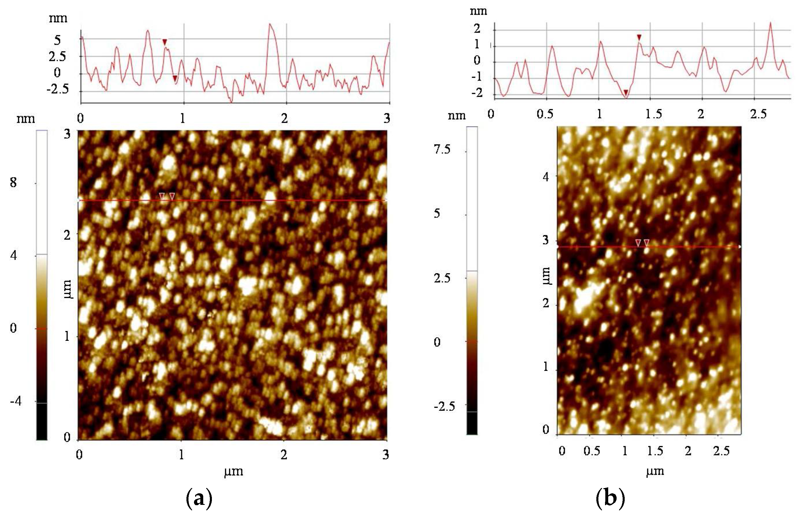
Moreover, surface morphology of the ITO/PEN and ITO/PET sheets after bending is also examined by AFM, and shown in Figure 11 and Figure 12. The surface roughness profiles along selected scanning paths in the investigated areas are also shown in Figure 11 and Figure 12. If cracks are present on the outer surface of ITO layer, it is expected that certain changes in the surface morphology would be observed through AFM. Therefore, scanning paths in the AFM are selected to pass across an apparent crack which is visible by OM. Although the selected scanning paths in the AFM pass across an apparent crack, both Figure 11b and Figure 12b reveal that the ITO outer surface has no remarkable change in the roughness profile along the scanning line. Note that the ITO layer is transparent. Therefore, the cracks observed in OM might be initiated at the interface of ITO/PET and ITO/PEN sheets, instead of at the outer surface of ITO layer. The AFM results indicate that cracks are not initiated at the ITO outer surface. A similar observation has been reported by Li and Lin [16] that cracks are preferentially initiated at the interface between ITO layer and substrate during bending.
Cross-sectional SEM micrographs of ITO/PEN and ITO/PET sheets are shown in Figure 13. As shown in Figure 13, the ITO layer thickness is about 200–250 nm for both cases. According to the product specifications, the overall thickness of the ITO/PEN and ITO/PET sheets is 200 μm [13] and 133 μm [52], respectively. As the thickness of ITO layer is comparable between the ITO/PEN and ITO/PET sheets, the bending effect on the ITO thin film is also related to the substrate structure. In this regard, stiffness and thickness of the substrate also play a role in the bending behavior of ITO thin film. As listed in Table 1, the Young’s modulus of PEN is greater than that of PET. Moreover, the substrate thickness in the ITO/PEN sheet is also greater than that in the ITO/PET sheet. As the Young’s modulus of PEN is greater than that of PET, it is expected that flexibility of PET is better than that of PEN.
In order to correlate the flexible deformation with bending stress, a three-dimensional (3D) finite element method (FEM) model is established to quantitatively determine the corresponding stress values in the bending test. The material properties and thicknesses of thin films used in the FEM modeling are listed in Table 1. Distributions of the maximum principal stress (σ1) in the ITO/PET and ITO/PEN sheets are then obtained for a similar bending radius of 10 mm, as shown in Figure 14. As shown in Figure 14, the ITO/PET or ITO/PET specimen is bent in a concave downward position, and the ITO thin layer on the top is under tension. In the comparison of ITO/PEN and ITO/PET sheets under tensile bending at a bending radius of 10 mm, σ1 in the ITO/PEN and ITO/PET sheets is 1309 MPa and 857 MPa, respectively (Figure 14). Note that the critical tensile fracture stress for ITO thin film is of 1.2 GPa [56]. Accordingly, the ITO/PEN sheet is expected to experience severe cracking right after applying a tensile bending of 10 mm curvature radius, as the calculated σ1 = 1309 MPa is greater than the critical tensile fracture stress. This is consistent with the experimental observation in which the electrical resistance significantly increases by 500% at the beginning of applying a tensile bending of 10 mm radius on the ITO/PEN sheet (Figure 3d). These calculations also show that ITO thin film in the ITO/PET sheet has a smaller stress at a given bending radius, compared to the ITO/PEN one. Based on the mechanics calculation of multilayer thin film under flexural deformation [57] and a critical tensile fracture stress of 1.2 GPa for ITO thin film [56], a limited bending radius of 9.6 mm and 6.1 mm is estimated for the given ITO/PEN and ITO/PET sheets, respectively, for an instantaneous bending failure. Therefore, the ITO/PEN sheet is seriously damaged under a tensile bending of 10 mm radius, and a significantly detrimental effect on the ITO/PET sheet is found for bending with a radius of curvature of 5 mm, as observed in the experiment. Based on the comparisons described above, the given ITO/PET sheet exhibits a greater resistance to long-term flexural deformation than the ITO/PEN sheet, in terms of degradation in the electrical conductance of ITO.

4. Conclusions

(1)
Tensile bending is much more detrimental than compressive bending to the electrical conductance of the given ITO/PEN and ITO/PET sheets under a long-term static flexural deformation.
(2)
Under tensile and compressive bending of a curvature radius of 30 mm or larger, electrical conductance of both ITO/PEN and ITO/PET sheets remain stable for up to 1000 h of static loading.
(3)
In 1000 h of tensile bending at a 20 mm curvature radius for the ITO/PEN sheet and at a 10 mm curvature radius for the ITO/PET sheet, the electrical conductance of ITO is degraded by 3–15% and 6–20%, respectively.
(4)
In 1000 h of tensile bending at a 10 mm curvature radius for the ITO/PEN sheet and at a 5 mm curvature radius for the ITO/PET sheet, the electrical conductance of ITO is significantly degraded by 800–900% and 60,000%, respectively.
(5)
The given ITO/PET sheet has a greater resistance to long-term mechanical bending than the ITO/PEN sheet in terms of change in electrical conductance. This is attributed to a smaller stress in the ITO layer because the ITO/PET sheet has a smaller stiffness and thickness in the substrate than the ITO/PEN sheet.

Author Contributions

C.-K.L. and H.-I.L. conceived and designed the experiments; H.-I.L. performed the experiments; D.-P.T. performed the numerical analysis; H.-I.L., C.-K.L., and D.-P.T. analyzed the data and wrote the paper.

Funding

This research was funded by the Ministry of Science and Technology (Taiwan) under contract no. MOST 105-2221-E-008-017-MY3.

Conflicts of Interest

The authors declare no conflict of interest.

References

  1. Greiner, M.T.; Lu, Z.-H. Thin-film metal oxides in organic semiconductor devices: Their electronic structures, work functions and interfaces. NPG Asia Mater. 2013. [Google Scholar] [CrossRef]
  2. Indium Tin Oxide (ITO) (In2O3):(SnO2), Indium Corporation. Available online: http://www.indium.com/inorganic-compounds/indium-compounds/indium-tin-oxide/ (accessed on 31 May 2018).
  3. Cao, W.; Li, J.; Chen, H.; Xue, J. Transparent electrodes for organic optoelectronic devices: A review. J. Photonics Energy 2014, 4, 040990. [Google Scholar] [CrossRef]
  4. Canhola, P.; Martins, N.; Raniero, L.; Pereira, S.; Fortunato, E.; Ferreira, I.; Martins, R. Role of annealing environment on the performances of large area ITO films produced by rf magnetron sputtering. Thin Solid Films 2005, 487, 271–276. [Google Scholar] [CrossRef]
  5. Gonçalves, G.; Grasso, V.; Barquinha, P.; Pereira, L.; Elamurugu, E.; Brignone, M.; Martins, R.; Lambertini, V.; Fortunato, E. Role of room temperature sputtered high conductive and high transparent indium zinc oxide film contacts on the performance of orange, green, and blue organic light emitting diodes. Plasma Process. Polym. 2011, 8, 340–345. [Google Scholar] [CrossRef]
  6. Alam, M.J.; Cameron, D.C. Optical and electrical properties of transparent conductive ITO thin films deposited by sol–gel process. Thin Solid Films 2000, 377, 455–459. [Google Scholar] [CrossRef]
  7. Ding, X.; Yan, J.; Li, T.; Zhang, L. Transparent conductive ITO/Cu/ITO films prepared on flexible substrates at room temperature. Appl. Surf. Sci. 2012, 258, 3082–3085. [Google Scholar] [CrossRef]
  8. Yu, S.; Yang, W.; Li, L.; Zhang, W. Improved chemical stability of ITO transparent anodes with a SnO2 buffer layer for organic solar cells. Sol. Energy Mater. Sol. Cells 2016, 144, 652–656. [Google Scholar] [CrossRef]
  9. Gil, Y.; Kim, H. Hybrid ITO transparent conductive electrodes embedded with Pt nanoclusters for enhanced output efficiency of GaN-based light-emitting diodes. Thin Solid Films 2016, 603, 307–312. [Google Scholar] [CrossRef]
  10. Tan, N.-N.; Hung, D.-T.; Anh, V.-T.; Kang, B.-C.; Kim, H.-C. Improved patterning of ITO coated with gold masking layer on glass substrate using nanosecond fiber laser and etching. Appl. Surf. Sci. 2015, 336, 163–169. [Google Scholar] [CrossRef]
  11. Park, S.-H.; Lee, S.-J.; Lee, J.-H.; Kal, J.; Hahn, J.; Kim, H.-K. Large area roll-to-roll sputtering of transparent ITO/Ag/ITO cathodes for flexible inverted organic solar cell modules. Org. Electron. 2016, 30, 112–121. [Google Scholar] [CrossRef]
  12. Lim, C.-Y.; Park, J.-K.; Kim, Y.-H.; Han, J.-I. Mechanical and electrical stability indium-tin-oxide coated polymer substrates under continuous bending stress condition. J. Int. Counc. Electr. Eng. 2012, 2, 237–241. [Google Scholar] [CrossRef]
  13. Peccell Product Information, Peccell Technologies, Inc. Available online: http://www.peccell.com/products/PECF/ (accessed on 31 May 2018).
  14. Ibeh, C.C. Thermoplastic Materials: Properties, Manufacturing Methods, and Applications; CRC Press: Cleveland, OH, USA, 2011. [Google Scholar]
  15. Kirubanandham, A.; Basu, S. On Characterization of Mechanical Deformation in Flexible Electronic Structures; Agilent Technologies, Inc.: Santa Clara, CA, USA, 2012. [Google Scholar]
  16. Li, T.-C.; Lin, J.-F. Fatigue life study of ITO/PET specimens in cyclic bending tests. J. Mater. Sci. Mater. Electron. 2014, 26, 250–261. [Google Scholar] [CrossRef]
  17. Li, T.-C.; Han, C.-F.; Chen, K.-T.; Lin, J.-F. Fatigue life study of ITO/PET specimens in terms of electrical resistance and stress/strain via cyclic bending tests. J. Display Technol. 2013, 9, 577–585. [Google Scholar] [CrossRef]
  18. Leterrier, Y.; Médico, L.; Demarco, F.; Månson, J.A.E.; Betz, U.; Escolà, M.F.; Kharrazi Olsson, M.; Atamny, F. Mechanical integrity of transparent conductive oxide films for flexible polymer-based displays. Thin Solid Films 2004, 460, 156–166. [Google Scholar] [CrossRef]
  19. Lin, Y.-C.; Shi, W.-Q.; Chen, Z.-Z. Effect of deflection on the mechanical and optoelectronic properties of indium tin oxide films deposited on polyethylene terephthalate substrates by pulse magnetron sputtering. Thin Solid Films 2009, 517, 1701–1705. [Google Scholar] [CrossRef]
  20. Hamasha, M.M.; Alzoubi, K.; Lu, S.; Desu, S.B. Durability study on sputtered indium tin oxide thin film on poly ethylene terephthalate substrate. Thin Solid Films 2011, 519, 6033–6038. [Google Scholar] [CrossRef]
  21. Lee, C.-C. Modeling and validation of mechanical stress in indium tin oxide layer integrated in highly flexible stacked thin films. Thin Solid Films 2013, 544, 443–447. [Google Scholar] [CrossRef]
  22. Jung, S.; Lim, K.; Kang, J.-W.; Kim, J.-K.; Oh, S.-I.; Eun, K.; Kim, D.-G.; Choa, S.-H. Electromechanical properties of indium–tin–oxide/poly(3,4-ethylenedioxythiophene): Poly(styrenesulfonate) hybrid electrodes for flexible transparent electrodes. Thin Solid Films 2014, 550, 435–443. [Google Scholar] [CrossRef]
  23. Machinaga, H.; Ueda, E.; Mizuike, A.; Takeda, Y.; Shimokita, K.; Miyazaki, T. Effects of annealing temperature on mechanical durability of indium-tin oxide film on polyethylene terephthalate substrate. Thin Solid Films 2014, 559, 36–39. [Google Scholar] [CrossRef]
  24. Kim, E.-H.; Yang, C.-W.; Park, J.-W. Improving the delamination resistance of indium tin oxide (ITO) coatings on polymeric substrates by O2 plasma surface treatment. Curr. Appl. Phys. 2010, 10, 510S–514S. [Google Scholar] [CrossRef]
  25. Hauger, T.C.; Zeberoff, A.; Worfolk, B.J.; Elias, A.L.; Harris, K.D. Real-time resistance, transmission and figure-of-merit analysis for transparent conductors under stretching-mode strain. Sol. Energy Mater. Sol. Cells 2014, 124, 247–255. [Google Scholar] [CrossRef]
  26. Saleh, M.N.; Lubineau, G. Understanding the mechanisms that change the conductivity of damaged ITO-coated polymeric films: A micro-mechanical investigation. Sol. Energy Mater. Sol. Cells 2014, 130, 199–207. [Google Scholar] [CrossRef]
  27. Van der Sluis, O.; Abdallah, A.A.; Bouten, P.C.P.; Timmermans, P.H.M.; den Toonder, J.M.J.; de With, G. Effect of a hard coat layer on buckle delamination of thin ITO layers on a compliant elasto-plastic substrate: An experimental–numerical approach. Eng. Fract. Mech. 2011, 78, 877–889. [Google Scholar] [CrossRef]
  28. Neerinck, D.G.; Vink, T.J. Depth profiling of thin ITO films by grazing incidence X-ray diffraction. Thin Solid Films 1996, 278, 12–17. [Google Scholar] [CrossRef]
  29. Chang, R.-C.; Tsai, F.-T.; Tu, C.-H. A direct method to measure the fracture toughness of indium tin oxide thin films on flexible polymer substrates. Thin Solid Films 2013, 540, 118–124. [Google Scholar] [CrossRef]
  30. Yang, C.-W.; Park, J.-W. The cohesive crack and buckle delamination resistances of indium tin oxide (ITO) films on polymeric substrates with ductile metal interlayers. Surf. Coat. Technol. 2010, 204, 2761–2766. [Google Scholar] [CrossRef]
  31. Kim, Y.-S.; Hwang, W.-J.; Eun, K.-T.; Choa, S.-H. Mechanical reliability of transparent conducting IZTO film electrodes for flexible panel displays. Appl. Surf. Sci. 2011, 257, 8134–8138. [Google Scholar] [CrossRef]
  32. Abdallah, A.A.; Bouten, P.C.P.; den Toonder, J.M.J.; de With, G. Buckle initiation and delamination of patterned ITO layers on a polymer substrate. Surf. Coat. Technol. 2011, 205, 3103–3111. [Google Scholar] [CrossRef]
  33. Boehme, M.; Charton, C. Properties of ITO on PET film in dependence on the coating conditions and thermal processing. Surf. Coat. Technol. 2005, 200, 932–935. [Google Scholar] [CrossRef]
  34. Can, M.; Havare, A.K.; Aydın, H.; Yagmurcukardes, N.; Demic, S.; Icli, S.; Okur, S. Electrical properties of SAM-modified ITO surface using aromatic small molecules with double bond carboxylic acid groups for OLED applications. Appl. Surf. Sci. 2014, 314, 1082–1086. [Google Scholar] [CrossRef] [Green Version]
  35. Han, D.; Lee, S.; Kim, H.; Jeong, S.; Yoo, S. Cathodic multilayer transparent electrodes for ITO-free inverted organic solar cells. Org. Electron. 2013, 14, 1477–1482. [Google Scholar] [CrossRef]
  36. Kim, D.-H.; Park, M.-R.; Lee, H.-J.; Lee, G.-H. Thickness dependence of electrical properties of ITO film deposited on a plastic substrate by RF magnetron sputtering. Appl. Surf. Sci. 2006, 253, 409–411. [Google Scholar] [CrossRef]
  37. Kim, E.-H.; Kim, G.; Lee, G.-H.; Park, J.-W. Nucleation and growth of crystalline indium tin oxide (ITO) coatings on polyethylene terephthalate (PET). Surf. Coat. Technol. 2010, 205, 1–8. [Google Scholar] [CrossRef]
  38. Lim, K.; Jung, S.; Kim, J.-K.; Kang, J.-W.; Kim, J.-H.; Choa, S.-H.; Kim, D.-G. Flexible PEDOT: PSS/ITO hybrid transparent conducting electrode for organic photovoltaics. Sol. Energy Mater. Sol. Cells 2013, 115, 71–78. [Google Scholar] [CrossRef]
  39. Minami, T. Present status of transparent conducting oxide thin-film development for indium-tin-oxide (ITO) substitutes. Thin Solid Films 2008, 516, 5822–5828. [Google Scholar] [CrossRef]
  40. Leppänen, K.; Augustine, B.; Saarela, J.; Myllylä, R.; Fabritius, T. Breaking mechanism of indium tin oxide and its effect on organic photovoltaic cells. Sol. Energy Mater. Sol. Cells 2013, 117, 512–518. [Google Scholar] [CrossRef]
  41. Tran, D.-P.; Lu, H.-I.; Lin, C.-K. Effects of cyclic deformation on conductive characteristics of indium tin oxide thin film on polyethylene terephthalate substrate. Surf. Coat. Technol. 2015, 283, 298–310. [Google Scholar] [CrossRef]
  42. Alkhazaili, A.; Hamasha, M.M.; Choi, G.; Lu, S.; Westgate, R. Reliability of thin films: Experimental study on mechanical and thermal behavior of indium tin oxide and poly(3,4-ethylenedioxythiophene). Microelectron. Reliab. 2015, 55, 538–546. [Google Scholar] [CrossRef]
  43. Peng, C.-Y.; Hamasha, M.M.; VanHart, D.; Lu, S.; Westgate, C.R. Electrical and optical degradation studies on AZO thin films under cyclic bending conditions. IEEE Trans. Device Mater. Reliab. 2013, 13, 236–244. [Google Scholar] [CrossRef]
  44. Hamasha, M.M.; Alzoubi, K.; Switzer, J.C.; Lu, S.; Poliks, M.D.; Westgate, C.R. Reliability of sputtered aluminum thin film on flexible substrate under high cyclic bending fatigue conditions. IEEE Trans. Compon. Packag. Technol. 2012, 2, 2007–2016. [Google Scholar] [CrossRef]
  45. Peng, C.-Y.; Dhakal, T.P.; Garner, S.M.; Cimo, P.; Lu, S.; Westgate, C.R. Strained growth of aluminum-doped zinc oxide on flexible glass substrate and degradation studies under cyclic bending conditions. IEEE Trans. Device Mater. 2014, 14, 121–126. [Google Scholar] [CrossRef]
  46. Hamasha, M.M.; Dhakal, T.P.; Vasekar, P.; Alzoubi, K.; Lu, S.; Vanhart, D.; Westgate, C.R. Reliability of sputter deposited aluminum-doped zinc oxide under harsh environmental conditions. Sol. Energy 2013, 89, 54–61. [Google Scholar] [CrossRef]
  47. Hamasha, M.M.; Alzoubi, K.; Lu, S. Behavior of sputtered indium–tin–oxide thin film on poly-ethylene terephthalate substrate under stretching. J. Display Technol. 2011, 7, 426–433. [Google Scholar] [CrossRef]
  48. Kim, J.-H.; Park, J.-W. Improving the flexibility of large-area transparent conductive oxide electrodes on polymer substrates for flexible organic light emitting diodes by introducing surface roughness. Org. Electron. 2013, 14, 3444–3452. [Google Scholar] [CrossRef]
  49. Park, J.-M.; Gu, G.-Y.; Wang, Z.-J.; Kwon, D.-J.; Devries, K.L. Interfacial durability and electrical properties of CNT or ITO/PVDF nanocomposites for self-sensor and micro actuator applications. Appl. Surf. Sci. 2013, 287, 75–83. [Google Scholar] [CrossRef]
  50. Tseng, S.-F.; Hsiao, W.-T.; Huang, K.-C.; Chiang, D.; Chen, M.-F.; Chou, C.-P. Laser scribing of indium tin oxide (ITO) thin films deposited on various substrates for touch panels. Appl. Surf. Sci. 2010, 257, 1487–1494. [Google Scholar] [CrossRef]
  51. Yu, Z.; Li, Y.; Xia, F.; Zhao, Z.; Xue, W. Properties of indium tin oxide films deposited on unheated polymer substrates by ion beam assisted deposition. Thin Solid Films 2009, 517, 5395–5398. [Google Scholar] [CrossRef]
  52. Product Specification of WT155hh, Win-Optical Technology Co., Ltd. Available online: http://www.win-optical.com.tw/products_cf.html (accessed on 31 May 2018).
  53. Busfield, J.; Thomas, A.; Yamaguchi, K. Electrical and mechanical behavior of filled rubber. III. Dynamic loading and the rate of recovery. J. Polym. Sci. Part B Polym. Phys. 2005, 43, 1649–1661. [Google Scholar] [CrossRef]
  54. Yamaguchi, K.; Busfield, J.; Thomas, A. Electrical and mechanical behavior of filled elastomers. I. The effect of strain. J. Polym. Sci. Part B Polym. Phys. 2003, 41, 2079–2089. [Google Scholar] [CrossRef]
  55. Shimamura, H.; Nakamura, T. Mechanical properties degradation of polyimide films irradiated by atomic oxygen. Polym. Degrad. Stab. 2009, 94, 1389–1396. [Google Scholar] [CrossRef]
  56. Crawford, G. Flexible Flat Panel Displays; Wiley: New York, NY, USA, 2005. [Google Scholar]
  57. Kim, N.; Graham, S. Development of highly flexible and ultra-low permeation rate thin-film barrier structure for organic electronics. Thin Solid Films 2013, 547, 57–62. [Google Scholar] [CrossRef]
Figure 1. Schematic diagram of static bending test setup and cross section of sample structure of indium tin oxide (ITO) thin film.
Coatings 08 00212 g001
Figure 2. Schematic diagram of in situ measurement of electrical resistance during static bending test of ITO thin film.
Coatings 08 00212 g002
Figure 3. Electrical resistance change of ITO/PEN (polyethylene naphthalate) sheet under static bending of various radii: (a) 40 mm; (b) 30 mm; (c) 20 mm; and (d) 10 mm.
Coatings 08 00212 g003
Figure 4. Electrical resistance change of ITO/PET (polyethylene terephthalate) sheet under static bending of various radii: (a) 30 mm; (b) 20 mm; (c) 10 mm; and (d) 5 mm.
Coatings 08 00212 g004
Figure 5. OM micrographs of ITO/PEN sheet after compressive bending with a 10 mm curvature radius for 1000 h: (a) viewed from PEN side; (b) viewed from ITO side.
Coatings 08 00212 g005
Figure 6. OM micrographs of ITO/PEN sheet after tensile bending with a 10 mm curvature radius for 1000 h: (a) viewed from PEN side; (b) viewed from ITO side.
Coatings 08 00212 g006
Figure 7. OM micrograph of ITO/PEN sheet after tensile bending with a 20 mm curvature radius for 1000 h, as viewed from the ITO side.
Coatings 08 00212 g007
Figure 8. SEM micrograph of ITO/PEN sheet after tensile bending with a 10 mm curvature radius for 1000 h, as viewed from the ITO side.
Coatings 08 00212 g008
Figure 9. OM micrograph of ITO/PET sheet after tensile bending with a 5 mm curvature radius for 1000 h, as viewed from the ITO side.
Coatings 08 00212 g009
Figure 10. SEM micrograph of ITO/PET sheet after tensile bending with a 5 mm curvature radius for 1000 h, as viewed from the ITO side.
Coatings 08 00212 g010
Figure 11. AFM images of ITO/PEN sheet: (a) as-received; (b) after tensile bending with a 10 mm curvature radius for 1000 h.
Coatings 08 00212 g011
Figure 12. AFM images of ITO/PET sheet: (a) as-received; (b) after tensile bending with a 5 mm curvature radius for 1000 h.
Coatings 08 00212 g012
Figure 13. Cross-sectional SEM micrographs of (a) ITO/PEN sheet and (b) ITO/PET sheet.
Coatings 08 00212 g013
Figure 14. Distributions of maximum principal stress in ITO thin film on (a) PET substrate and (b) PEN substrate.
Coatings 08 00212 g014
Table 1. Material properties and parameters used in the 3D FEA modeling [12,13,14].
MaterialYoung’s Modulus (GPa)Poison RatioThickness (μm)
ITO1160.350.25
PET3.00.37133
PEN6.10.38200