Factors Affecting Electroplated Semiconductor Material Properties: The Case Study of Deposition Temperature on Cadmium Telluride


1
Department of Mechanical Engineering, Ekiti State University (EKSU), Ado-Ekiti 360211, Nigeria
2
Electronic Materials and Sensors Group, Materials and Engineering Research Institute (MERI), Sheffield Hallam University, Sheffield S1 1WB, UK
*
Author to whom correspondence should be addressed.
Coatings 2019, 9(6), 370; https://doi.org/10.3390/coatings9060370
Submission received: 9 April 2019
/
Revised: 25 May 2019
/
Accepted: 4 June 2019
/
Published: 7 June 2019
(This article belongs to the Special Issue Advanced Thin Film Materials for Photovoltaic Applications)
Abstract
:Electrodeposition of cadmium telluride (CdTe) on fluorine doped tin oxide (FTO) using two electrode configurations was successfully achieved with the main focus on the growth temperature. The electroplating temperatures explored ranged between 55 and 85 °C for aqueous electrolytes containing 1.5 M cadmium nitrate tetrahydrate (Cd(NO3)2·4H2O) and 0.002 M tellurium oxide (TeO2). The ensuing CdTe thin-films were characterized using X-ray diffraction (XRD), UV-Vis spectrophotometry, scanning electron microscopy (SEM), energy dispersive X-ray (EDX), and photoelectrochemical (PEC) cell measurements. The electroplated CdTe thin-films exhibit a dominant (111) CdTe cubic structure, while the crystallite size increases with the increase in the electroplating temperature. The dislocation density and the number of crystallites per unit area decrease with increasing growth temperature. The optical characterization depicts that the CdTe samples show comparable absorbance and a resulting bandgap of 1.51 ± 0.03 eV for as-deposited CdTe layers. A marginal increase in the bandgap and reduction in the absorption edge slope towards lower deposition temperatures were also revealed. The annealed CdTe thin-films showed improvement in the energy bandgap as it tends towards 1.45 eV while retaining the aforementioned absorption edge slope trend. Scanning electron microscopy shows that the underlying FTO layers are well covered with increasing grain size observable relative to the increase in the deposition temperature. The energy dispersive X-ray analyses show an alteration in the Te/Cd relative to the deposition temperature. Higher Te ratio with respect to Cd was revealed at deposition temperature lower than 85 °C. The photoelectrochemical cell study shows that both p- and n-type CdTe can be electroplated and that deposition temperatures below 85 °C at 1400 mV results in p-type CdTe layers.
1. Introduction
Electrodeposition has emerged as a one of the versatile and cost-effective growth techniques of metal, metalloid, and semiconductor materials [1]. With emphasis on semiconductor growth, the use of either two- or three- electrode electroplating technique has been effective in the growth of high-performance semiconductor materials [2]. Aside from the the electroplating configuration, challenging factors affecting the reproducibility of electroplated materials include the solutes incorporated and solvent utilized, electrolytic bath ionic concentrations, solution aging (electroplating age), the stabilities of both growth pH and deposition temperature, and the deposition current density [3]. Provided these factors are optimized, high-quality semiconductor materials such as cadmium telluride (CdTe) thin-films can be grown and incorporated for different applications. CdTe is one of the II-VI semiconductor materials that has been grown using several techniques including electroplating [4,5] and has been extensively researched owing to its properties [6]. Due to the direct bandgap of CdTe at room temperature (~1.45 eV), it is capable of absorbing a substantial fraction of the electromagnetic spectrum under AM1.5 conditions. This characteristic has been explored in the photovoltaic (PV) community in achieving high-efficiency CdTe-based solar cells [7]. The recent hike in the conversion efficiency from 16.5% in 2004 [8] to 22.1% in 2016 [9] as reported in the literature is mainly due to the eradication of defects within the crystal lattice or traps within the bandgap in addition to improved crystallinity, passivation of the grain boundaries which is due to better understanding of both material and device issues. Therefore, it is fundamental to strive towards process optimization amongst others. Under both two and three- electrode electrodeposition configurations, different deposition temperatures have been utilized by independent researchers [10,11,12,13,14,15,16] without a unifying examination of the effect of electroplating temperature in aqueous solution. Although, limiting factors such as the operating temperature of reference electrode (of about 70 °C) is to be considered for the three-electrode configurations. Therefore, this publication examines the effect of temperature of the electrolyte on the structural, optical, morphological compositional properties and electronic properties of electrodeposited CdTe layers grown from an aqueous solution containing tellurium dioxide (TeO2) and cadmium nitrate Cd(NO3)2 as the respective precursors of Te and Cd.
2. Materials and Methods
2.1. Thin-Film Synthesis
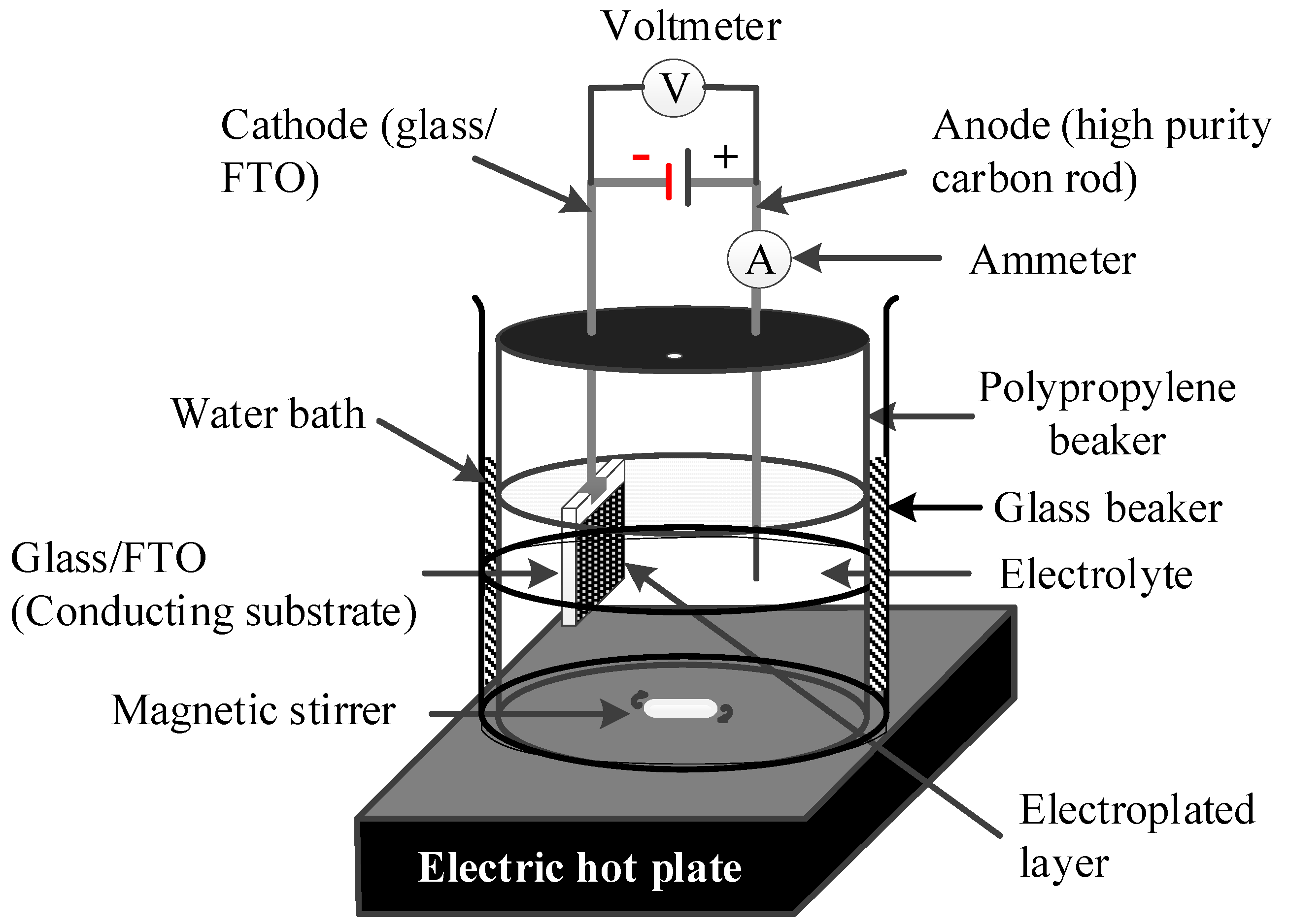
Cadmium telluride thin-films were electrodeposited from a solution containing 1.5 M cadmium nitrate tetrahydrate (Cd(NO3)2·4H2O) and 0.002 M tellurium oxide (TeO2). The respective precursors for Cd and Te were dissolved in 400 mL of deionized (DI) water contained in a polypropylene beaker using the set up depicted in Figure 1. The resulting aqueous solution will be referred to as CdTe-bath henceforth in this report. Using these precursor concentrations and electrolytic cell set up, four electrolytic baths were created. To achieve a transparent and homogenous solution, the baths were stirred for about 300 min.
Prior to electroplating, the pH and the magnetic stirring rate of the bath were maintained at 2.00 ± 0.02 and ~300 rpm. The adjustment of the pH is achieved by either using nitric (HNO3) acid to lower the pH value or ammonium hydroxide (NH4OH)—an alkaline to increase the pH value. The deposition temperature is set at 55, 65, 75, and 85 °C for respective electrolytic baths, while the deposition voltage is kept constant at 1400 mV for all the CdTe layers. The 1400 mV cathodic growth voltage is based on prior optimization of CdTe thin-films grown from a pure Cd(NO3)2 electrolyte as described in the literature [17]. The deposition temperature lower or higher than this range were not reported due to low adhesion of the ED-CdTe thin-film and the formation of water bubbles on the g/FTO substrate due to the close proximity of the deposition temperature to the boiling point of water.
The glass/fluorine-doped tin oxide (g/FTO) substrates utilized as the working electrode were cut into strips with a dimension of 3 × 2 cm2. The g/FTO strips were washed using soap water in an ultrasonic bath, alcohol, rinse thoroughly in DI water and dried using nitrogen gas [18]. After the thin-film layer deposition, the 3 × 2 cm2 strips were cut into two halves of 3 × 1 cm2. One half is left as-deposited (AD) while the other is cadmium chloride treated (CCT) to improve the material and electronic properties of the CdTe layers as it used in the CdTe-based photovoltaic device-ready process. The CCT treatment was performed by adding a few drops of aqueous solution containing 0.1 M CdCl2 in 20 mL of DI water to the CdTe surface. The full coverage of the CdTe layers with the CdCl2 solution was achieved by spreading the solution using solution-damped cotton bud. The CdTe layers were allowed to air-dry and annealed afterwards in air at 400 °C for 20 min. The CCT-CdTe layers were allowed to cool in the air before both the AD and the CCT layers were rinsed to eliminate the loosely adhered particles of CdTe, Cd, and Te from the surfaces of the thin-film and dried in the presence of nitrogen gas.
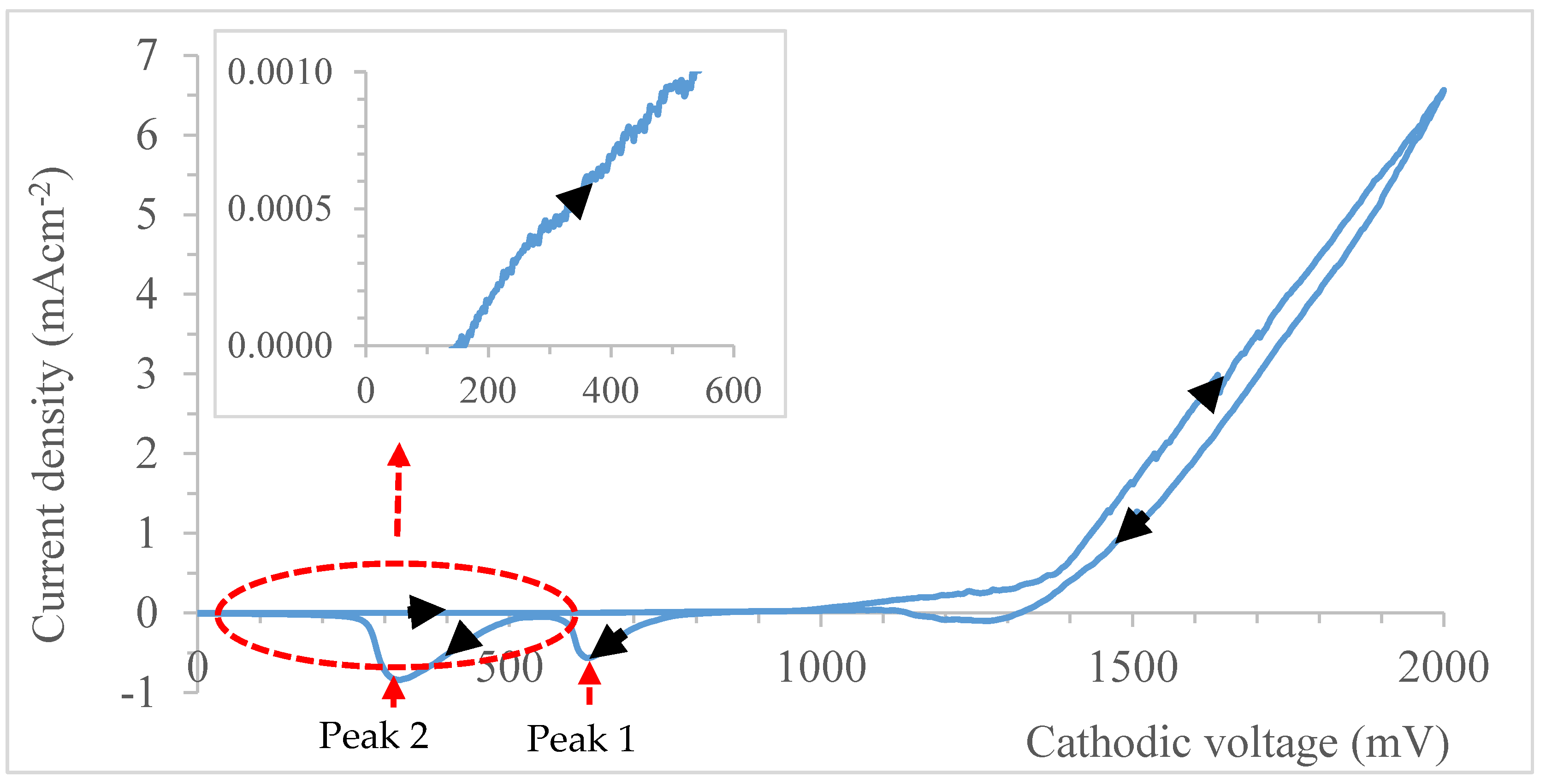
It is necessary to note that cyclic voltammetry as shown in Figure 2 of the CdTe-bath was performed at electrolytic bath conditions when bath temperature, pH, and stirring rate were set at 85 °C, 2.00 ± 0.02 and ~300 rpm. The voltammogram is the current-voltage (I-V) curve of the CdTe-bath to determine the optimal cathodic voltage region for the deposition of CdTe.
Tellurium is deposited first because it is more positive as compared to cadmium with respective standard reduction potential value of +593 mV and −403 mV with respect to standard H2 electrode. From the inset of Figure 2, Te starts depositing at a cathodic voltage of ~170 mV and above, while Cd starts deposition at 1000 mV. Details of the optimization process have been documented by the author’s group in the literature [12,17].
2.2. Thin-Film Characterization
The electroplated layer characterisation were performed using equipment made available by the Materials and Engineering Research Institute (MERI) research institute, Sheffield Hallam University (SHU), UK.
The structural characterization was carried out using Philips PW 3710 X’pert diffractometer (Almelo, Netherlands) mounted with 1.5406 Å wavelength Cu-Kα monochromator. The X-ray diffraction system is also equipped with X’Pert High Score which aided with phase identification, dominant diffraction and for the estimation of the crystallite sizes. For the experiments presented in this work, thin-films were scanned between the range of 2θ = 20°–70°. Using the Scherrer formula as shown in Equation (1), the crystallite size D was estimated. Where β denotes the full-width-at-half-maximum (FWHM) of the diffraction intensity in radians, θ denotes the Bragg angle, λ denotes the X-rays wavelength (which is 1.5406 Å for Cu-Kα monochromator) and K is the shape constant. For spherical geometry, K is taken as 0.94.
The dislocation density, δ, which defines the length of dislocation lines per unit volume of crystal in the thin-film is calculated using Equation (2) as reported in the literature [19]
The estimation of the number of crystallites per unit area in the thin-film, N, was done using Equation (3) as documented in [19,20].
The film thickness was measured using a UBM 1080 Microfocus optical profilometer (UBM Messtechnik, Koln, Germany) and mathematically estimated using Faraday’s law of electrolysis (see Equation (4)), where T is the film thickness, J is the average current density during deposition, M is the molar mass of CdTe (MCdTe = 240.01 gmol−1), t is the duration of deposition, n is the number of electrons transferred for deposition of 1 molecule of CdTe (n = 6), and F is the constant defined by Faraday as 96,485 Cmol−1, and ρ is the density of CdTe.
The optical absorbance data of the electroplated thin-films were taking within the range of 200 to 800 nm using Cary50 Scan UV-visible spectrophotometer (Agilent Technologies, Santa Clara, CA, USA). From the absorbance data accumulated within the specified wavelength range, the bandgap was estimated using the Tauc’s formula illustrated in Equation (5) via the graph of (αhv)2 versus (hv). Where the coefficient of absorption is represented by α, the bandgap energy is represented by Eg, the Planck’s constant is represented by h, the incident photon frequency is represented by v, the proportionality constant which depends on the refractive index of the sample under investigation is represented by k, and m equals 0.5 for a direct bandgap semiconductor. The extrapolation of the straight line portion of the Tauc’s plot (at (αhv)2 = 0) gives the bandgap energy.
The examination of the thin film’s surface morphology and composition was performed in vacuum condition using FEI Nova200 NanoSEM (Electron Nanoscopy Instrument, Lincoln, NE, USA) fitted with energy dispersive X-ray (EDX) detector. The confirmation of the electrical conduction type is done using photoelectrochemical (PEC) cell measurements by the formation of a junction between the solid (g/FTO/CdTe) and liquid (an aqueous solution of 0.1 M Na2S2O3 in 20 mL DI water). The comprehensive detail of the PEC set up is incorporated in [18].
3. Result and Discussion
Material Characterization: In order to validate the results in this Section, all the stated values correspond to the average of three replica samples investigated under the same conditions.
3.1. X-Ray Diffraction (XRD) Analysis
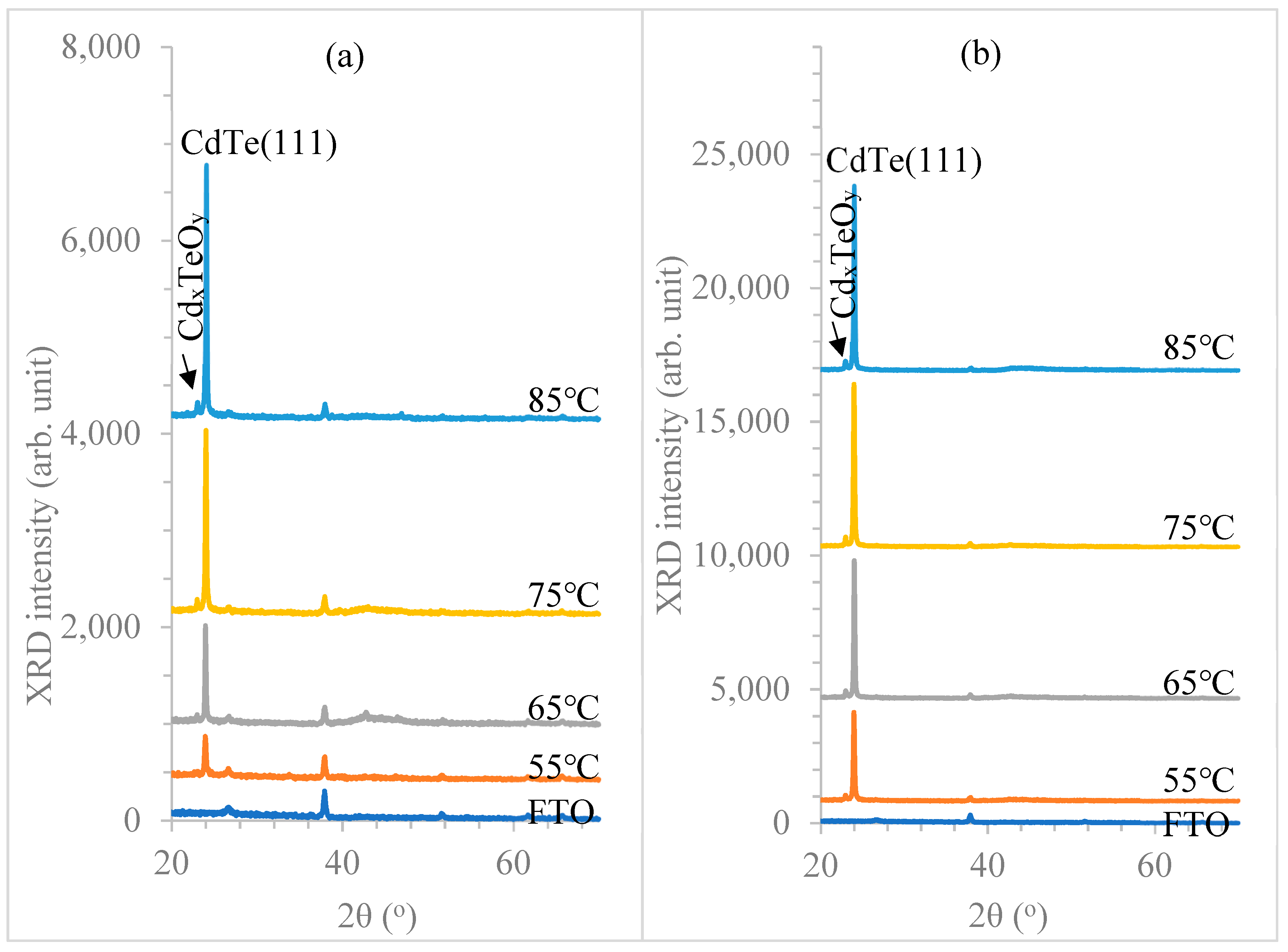
For this set of experiments, the thicknesses of the CdTe layers electrodeposited at a different temperature from CdTe-baths was maintained at ~1µm under as-deposited conditions using factors such as deposition time, stirring rate amongst others. Figure 3a,b illustrate the typical XRD patterns of CdTe thin-films electrodeposited at different growth temperatures under as-deposited (AD) and cadmium chloride treated (CCT) conditions respectively. While Table 1; Table 2 are the respective summaries of the X-ray diffraction analysis for cubic (111) CdTe diffraction for AD and CCT-CdTe layers and the comparative analysis of the dislocation density and number of crystallites per unit area of the CdTe thin-films electroplated at a different temperature. Under both the AD and CCT conditions, the CdTe layers show diffraction patterns with a preferential and strong (111) phase of the cubic structure of CdTe at 2θ = ~24.0° (see Figure 3a,b). Diffractions with the underlying g/FTO substrate were observable at 2θ = ~20.6°, ~33.8°, ~37.9°, ~51.6°, ~60.7° and ~65.6°. This is in addition to the cadmium tellurate (CdxTeOy) diffraction observed at 2θ = 23.0°. With respect to the AD-CdTe layers shown in Figure 3a and Table 1, an increase in the deposition temperature resulted in an increase in the cubic (111) CdTe diffraction intensity, peak sharpness, and crystallite size as evident by the 65.8 nm observed at 85 °C. This indicates an enhancement in the crystallinity and a reduction in the lattice defects of the CdTe-layers at high deposition temperature. This observation can also be said of the CCT-CdTe layers with the highest cubic (111) CdTe intensity at 85 °C (see Figure 3b and Table 1).
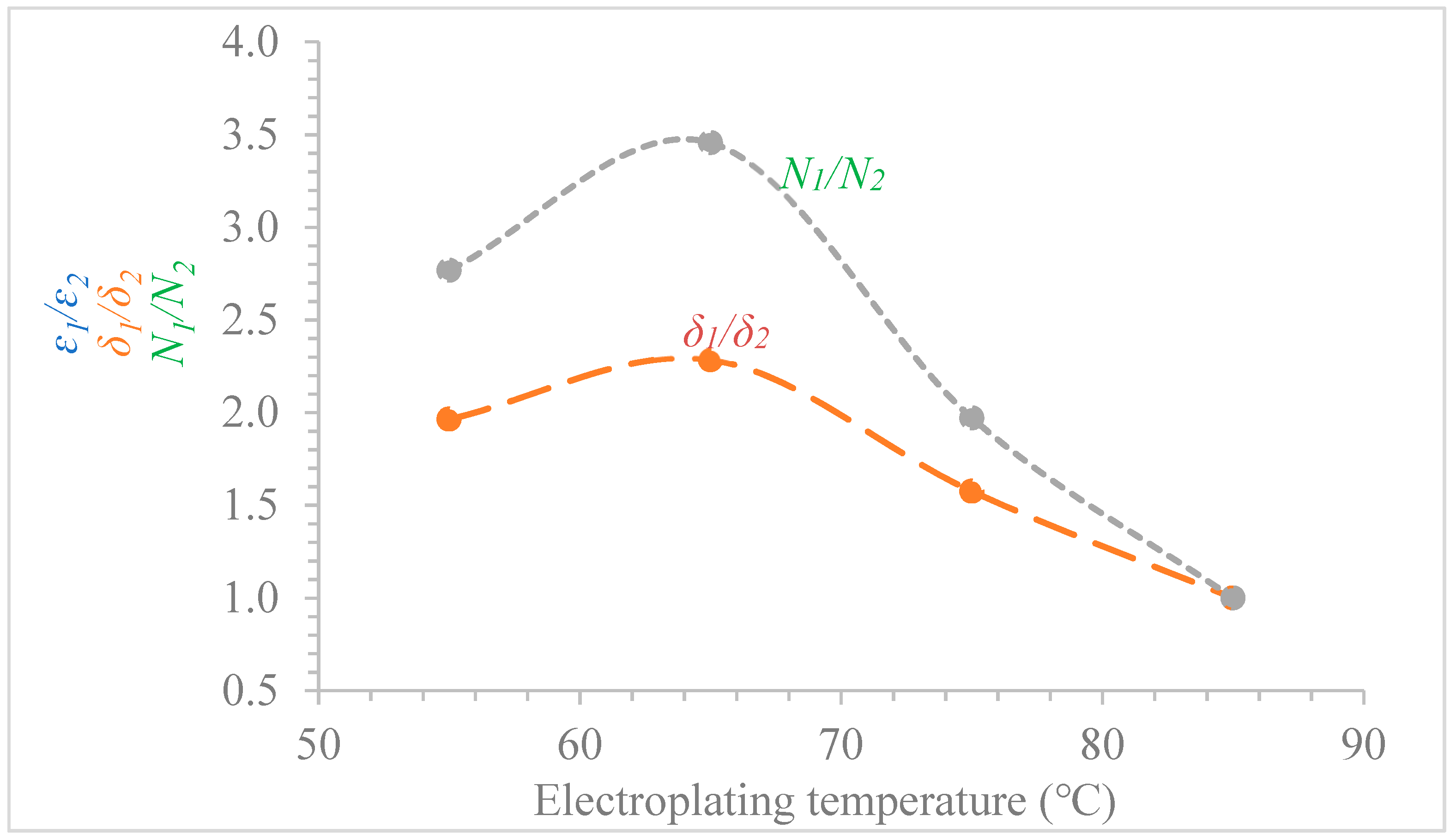
With emphasis on the CdTe (111)C preferred orientation, a drastic improvement in the intensity of the diffraction after CCT treatment and crystallite size was observed notwithstanding the CdTe-bath deposition temperature. Interestingly, a reduction in the dislocation density and the number of crystallites per unit area was observed with an increase in the deposition temperature, while further improvements were observed even after CCT (see Table 2 and Figure 4). This observations might be as a result of the recrystallization of the polycrystalline CdTe thin-films during treatment which results to the improvement in the Cd/Te stoichiometry by the sublimation of surplus elements or the formation of CdTe by the reaction between surplus elemental Te and Cd from CdCl2 treatment [4,21]. It should be noted that no matter the deposition technique, Te –precipitation is one of the main challenges in the deposition of CdTe [22,23]
Improvement in the crystallinity of CdTe after post-growth treatment in the presence of chlorine due to factors such as grain growth, recrystallization amongst others is generally accepted by the scientific community [24,25]. The stagnation observed in the crystallite size at 65.8 nm might be as a result of the limitation of the XRD machine utilized and/or that of the Scherrer’s formula utilized in the measurement and analysis of CdTe thin-films respectively [26,27].
The obtained XRD diffraction data from the CdTe thin film structural analysis is in agreement with the 01-075-2086 reference file of the Joint Committee on Powder Diffraction Standards (JCPDS) for cubic CdTe layers.
3.2. Thickness Measurement
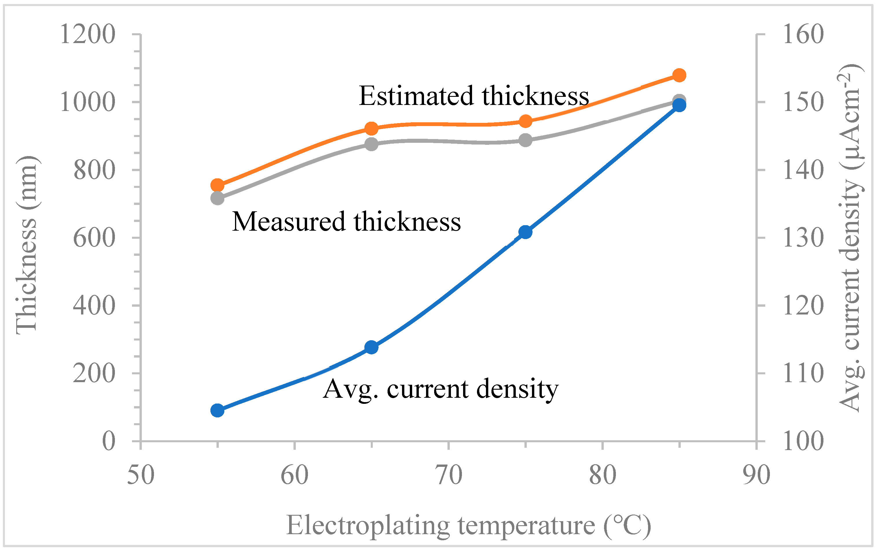
For this experiment, the deposition duration was maintained at 180 min for each of the electroplated CdTe at different deposition temperatures. Figure 5 shows the graphical plot of both the estimated and the measured thicknesses including the average deposition current density of the CdTe layers against the deposition temperature. For the estimated thickness using the Faraday’s equation (see Equation (4)), the rise in the thickness of electrodeposited CdTe with increasing deposition temperature was solely due to the corresponding increase in the average current density of deposition. In addition, increase in the solubility of solvents and the catalyses, the reactions are also as a result of an increase in the electroplating temperature [28]. Correspondingly, this divulges an increase in the deposition current density and hence, a rapid growth rate of constituent elements or compounds.
The observed deviation of the estimated thickness and the measured thickness is due to the assumption made by Faraday’s law of electrolysis that all the electronic charges flowing through the electrolytic cell partake in the growth of the electroplated materials. The assumption did not consider the electronic charges associated with the breakdown of water into its constituent ions and the additional chemical reactions on both the cathode and anode. Therefore, the estimated thickness using Faraday’s formula served as the upper limit of the thickness. As observed in Figure 5, a greater deviation between the measured and the estimated thickness was observed for the CdTe layers grown at 85 °C due to the favourable impact of higher temperature to molecular and ionic activity within the electrolyte.
3.3. Optical Properties Analysis
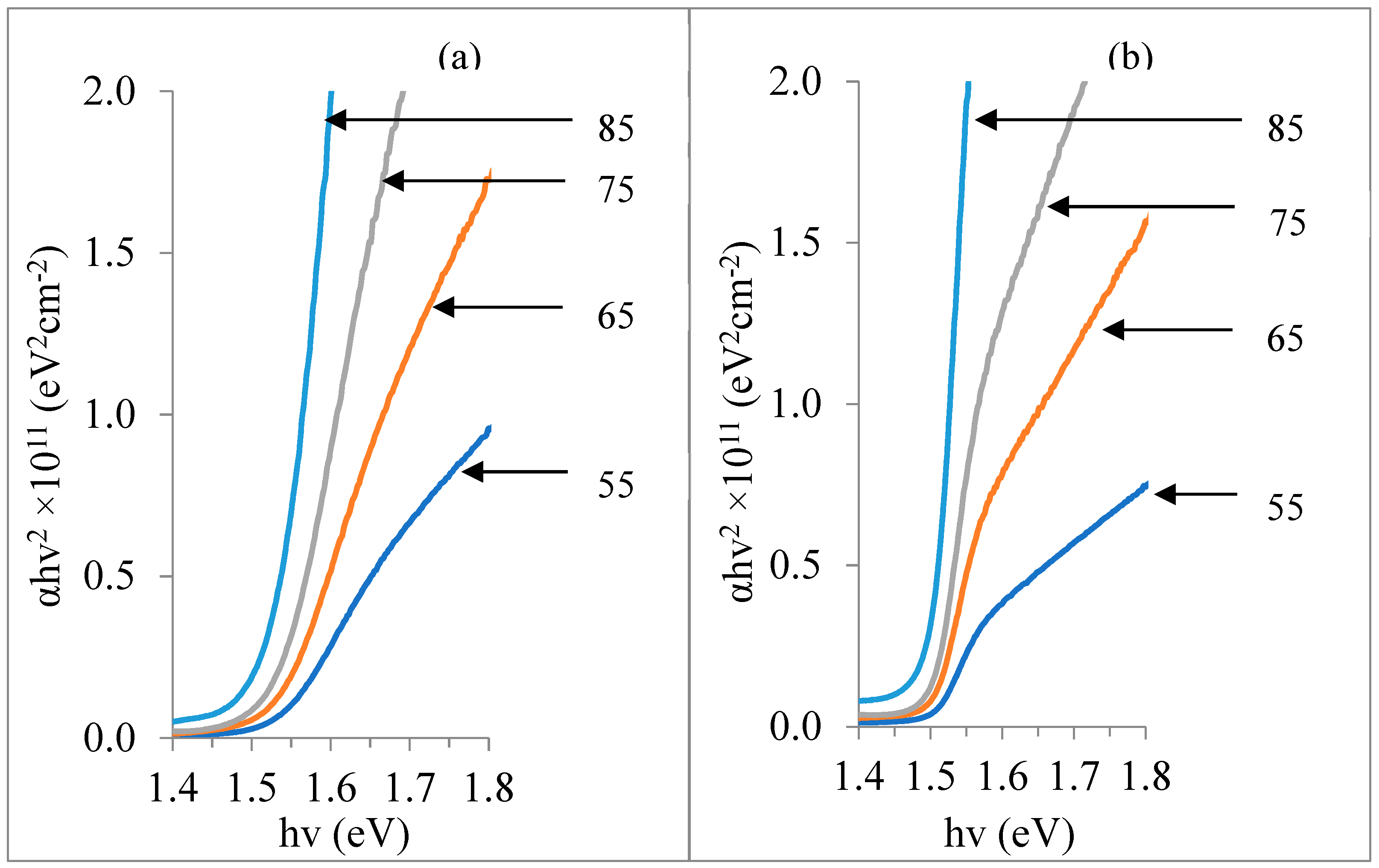
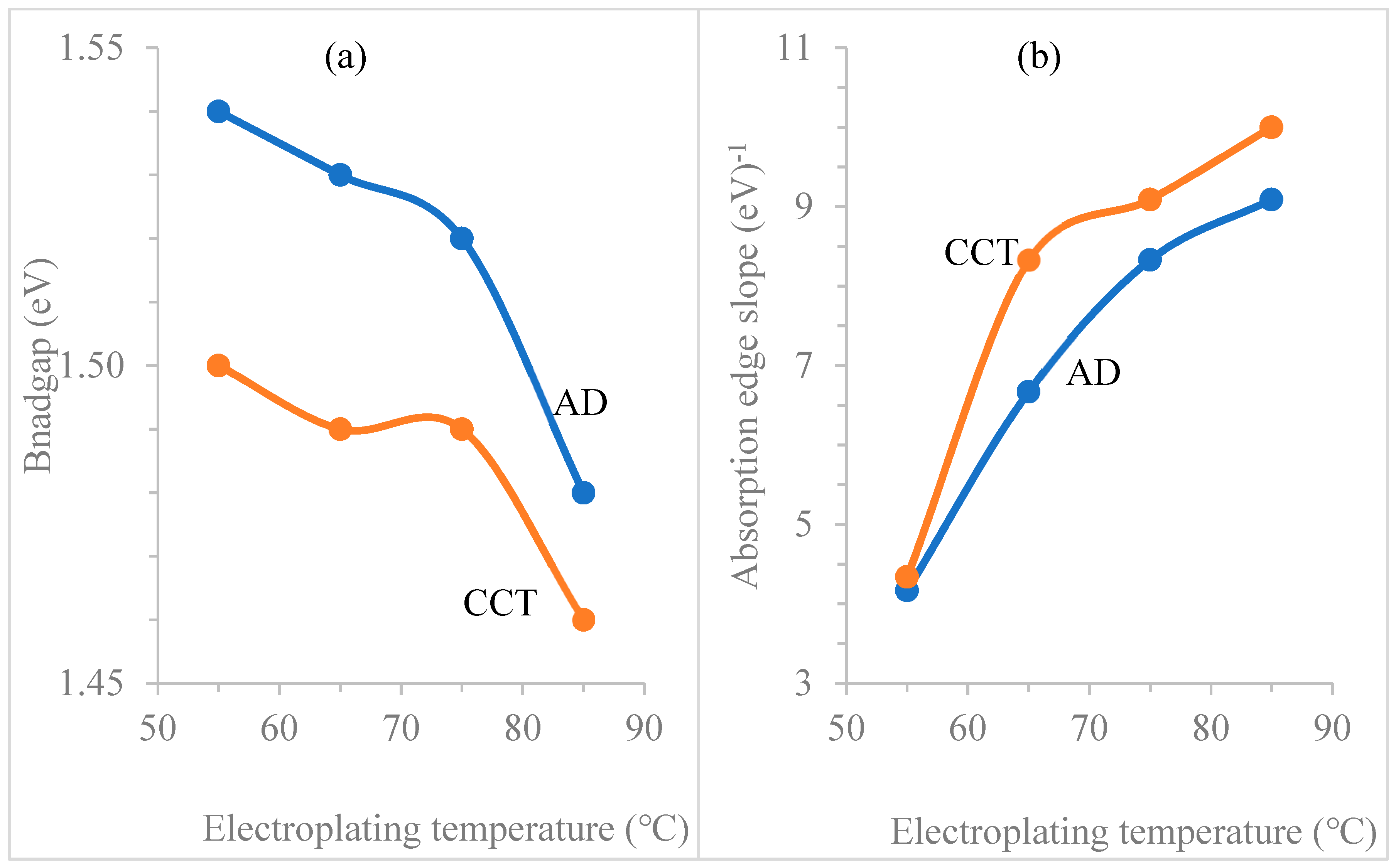
Figure 6a,b shows the Tauc’s plot of (αhv)2 against (hv) for CdTe thin-films electrodeposited at different temperatures under both AD and CCT conditions respectively. Table 3 and Figure 7 summarizes the observed bandgap energy and the absorption edge of the investigated CdTe thin-films. Under the as-deposited condition, the observed bandgaps range is within the generally acceptable range of 1.51 ± 0.03 eV for CdTe layers [29]. This follows a trend in which the highest bandgap of 1.54 eV was recorded at 55 °C and the lowest bandgap of 1.48 eV was observed at 85 °C. It is generally accepted in the photovoltaic community that the optimal bandgap 1.45 eV is required to achieve the highest efficiency of a one-bandgap p-n junction photovoltaic device.
A shift towards 1.45 eV bandgap was observed after post-growth treatment –CCT as shown in Figure 6b, Figure 7 and Table 3. This observation should be as a result of the improvement in the material and electronic properties of CdTe [24,25]. Further to this, a shift in the absorption edge slope was also observable, with the highest edge slope observed at 85 °C under both AD and CCT conditions. It is known that the sharpness of the absorption edge slope indicates lesser impurity energy levels and defects in the thin-films under investigation [30,31,32,33]. This observation suggests that more stoichiometric CdTe layers are deposited at 85 °C and a further improvement is achievable after CCT. This observation is in agreement with the summation made in Section 3.1.
3.4. Morphological Properties Analysis
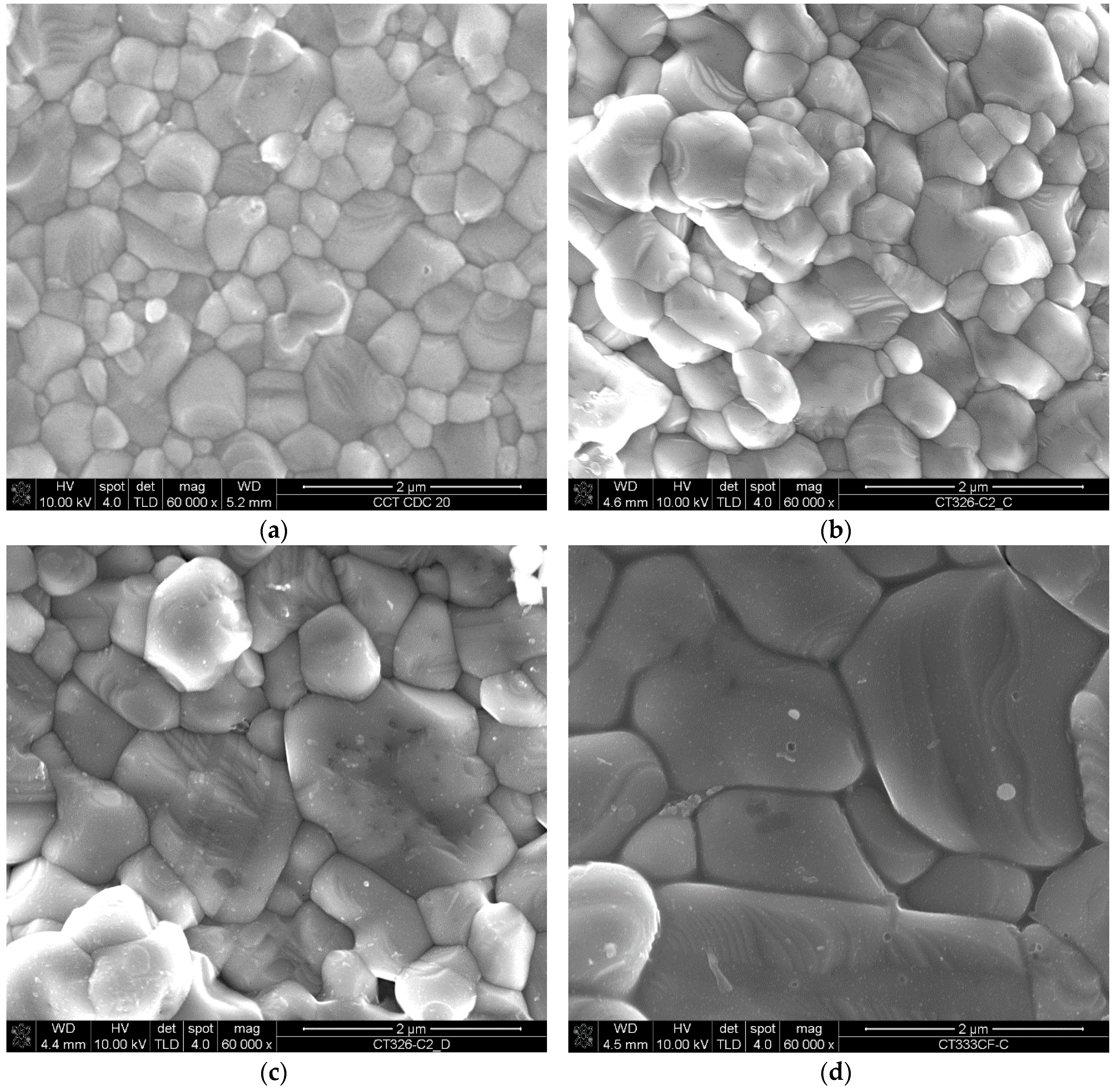
Figure 8a–d shows the SEM images of CCT-CdTe thin-films electrodeposited at different growth temperatures ranging from 55 to 85 °C. The CdTe thin-films deposited at all the explored deposition temperatures show excellent coverage of the underlying g/FTO substrate. The purported good coverage is due to the good quality of the CdTe layers deposited based on the electrodeposition parameters such as the cathodic voltage, stirring rate, pH amongst other factors prior to CCT. While the retention of the complete coverage after CCT is owing to the enhancements in the CdTe micro-structure as a result of the recrystallization, sublimation of superfluous elements, grain growth and the formation of CdTe via a chemical reaction between excess Cd from CdCl2 and precipitated Te in the layer. In AD-CdTe, cauliflower-like clusters consisting of numerous crystals are often observed with sizes ranging between ~30 and 65 nm [17]. Upon CCT, these crystals merge into grains due to their large surface to volume ratio. This is a key feature of nano-materials and helps in the formation of large grains. The CCT-CdTe grains are much larger with grains sizes ranging between ~200 and 6000 nm.
Based on topological observation, a gradual increase in the grain size with increasing deposition temperature was noted with the largest grain size of 6 µm and lower grain boundary density observed for the 85 °C bath. This observation indicates that although CCT facilitates grain growth in CdTe, high deposition temperature favours grain growth. It is relevant at this point to compare the noted trend of the grain size in Figure 8 with the deductions made based on the number of crystallites per unit area N1 in Section 3.1. It is at this point important to note that the calculated crystallite size using the Scherrer formula in XRD analysis does not translate to the sizes of grains observed in the SEM micrograph. However, grains can be formed from a single or multiple crystallites.
3.5. Compositional Measurement
Figure 9 shows the typical EDX spectra for AD and CCT-CdTe grain at 85 °C and the plot of the atomic composition ratio of Te to Cd in electroplated CdTe layers under both AD and CCT conditions against the electroplating temperature. Aside from Te and Cd elements, other elements such as O, F, Sn, Si were also randomly observed owing to layer oxidation and/or the underlying g/FTO substrate. With emphasis on the as-deposited CdTe layers as shown in Figure 9, the compositional ratio of Te/Cd is less than 1 for the CdTe thin-film deposited at 85 °C. The CdTe thin-films grown at deposition temperature 75 °C and below show comparative Te-richness.
It can be recalled from the succinct discussion on the cyclic voltammogram in Section 2.1 and Figure 2 that with the increasing deposition potential, electroplated layers go through the stages of Te deposition, Te-rich CdTe deposition, near stoichiometric CdTe deposition and Cd-rich CdTe depositions based on the redox potential of Cd and Te. The observed effect of deposition temperature even when it is performed at the same deposition potential seems to give a similar effect by a continued shift in the cyclic voltammetric graph to the right with decreasing deposition temperature. This argument is valid due to the catalytic effect of heat in reaction and in the mobility of ions constituted in the electrolyte especially Cd with comparatively lower redox potential. This is one of the possible reasons for the Cd or Te richness of the deposited CdTe layer at the same cathodic voltage at the exploring temperature of 85 °C and between 55 and 85 °C, respectively. After CCT, a shift towards stoichiometry in the atomic composition ratio of the CdTe layers was observed (see Figure 9). This might be influenced by the reaction between Cd from CdCl2 with unreacted Te and/or the sublimation of excess elemental Cd and Te from the layer. For photovoltaic applications, the richness of Cd in CdTe used as an absorber layer has been documented in the literature to produce a comparatively higher efficiency [34,35,36,37]. A stoichiometry of 50/50 Te to Cd atomic composition was observed for the 85 °C CdTe after CCT signify comparatively higher crystallinity. This observation is in agreement with the high crystallinity level observed at 85 °C.
3.6. Photoelectrochemical (PEC) Cell Measurement
Figure 10 shows the PEC cell measurements of the CdTe layers electroplated from electrolytes at different deposition temperature against electroplating temperature under both AD and CCT conditions. An all-round technique such as the Hall effect measurement was not used because of the effect of the highly conductive FTO underlying substrate. The obtained data cannot be isolated only for CdTe from the measurement.
As depicted in Figure 10, the electrical conduction type of the as-deposited CdTe layers grown at 85 °C is n-type while the ones grown at between 55 and 75 °C, are p-type. A similar observation is also made of the CdTe layers after CCT with a shift from the n-type layers towards p-type electrical conductivity and vice versa, while the initial conduction types were retained. The observed PEC signal shift after CCT is an attribute of recrystallization amongst factors that have been well document [24,25]. It is captivating that the observed PEC trend is somewhat similar to that of the EDX spectra summary in Figure 9c. This is because one of the predominant factors determining the electrical conduction type is the atomic compositional ratio of the constituent elements, with Te-richness in CdTe resulting in p-type and Cd-richness resulting in n-type conduction type [18,34,35]. Other factors include the heat treatment parameters (such as duration, temperature), preliminary atomic composition of Cd and Te, the concentration of CdCl2 or other dopants utilized in treatment, the structure of the defects in the material, and the initial conductivity type of the material [10,17,24,38].
4. Conclusions
The effect of deposition temperature in a two-electrode electrodeposition configuration was explored and the ensued CdTe thin-films were methodically characterized and presented. The structural, optical, morphological, compositional, and electronic properties of the CdTe relative to their deposition temperature were studied. All the electroplated thin-films grown at a different deposition temperature of the electrolyte show polycrystalline cubic structure of the material with a preferred orientation along the (111) plane. The dislocation density for the as-deposited CdTe was observed to be 7.15 × 10¹¹ lines·cm−2 for the CdTe deposited at 55 °C and 2.31 × 10¹¹ lines·cm−2 for the grown CdTe at 85 °C, which was respectively reduced to 3.64 and 2.31 lines·cm−2. The number of crystallites per unit area N was found to reduce from 1.91 × 10¹² to 0.35 × 1012 cm−2 with increased deposition temperature from 55 to 85 °C. The N was found to reduce to 0.69 × 10¹² to 0.35 × 1012 cm−2 with increased deposition temperature from 55 to 85 °C after CCT. This is an indication that the crystallite sizes increases after annealing. This was evident with the crystallite sizes of the as-deposited films ranging from 37.4 to 65.8 nm with increased deposition temperature from 55 to 85 °C to 52.4 to 65.8 nm after post-growth CCT. The optical property investigation reveals that, the deposited layers possess bandgaps ranging between 1.51 ± 0.03 eV under as-deposited condition and 1.48 ± 0.02 eV after CCT. Prominently, the sharpness of the optical absorption edge slope reduces with the reduction in the deposition temperature. Morphologically, all the electrodeposited layers show full underlying layer coverage. Comparatively, larger grains after CCT were observed for layers grown at 85 °C. The compositional analysis reveals the presence of Cd and Te in the deposited thin-film. A atomic ratio for Cd:Te of 1:1 was recorded for CdTe layers grown at an electroplating temperature of 85 °C. Additionally, an increase in the atomic concentration of Te with the reduction of the electroplating temperature for the explore deposition temperature range of 85 to 55 °C was noted. The PEC measurements show that the CdTe layers grown at 85 °C is n-type under both AD and CCT conditions, while p-type conduction type CdTe layers ensued for the layers grown at deposition temperature of 75 °C and below. These results underline the importance of the deposition temperature in the electrodeposition and the capability of two-electrode electrodeposition configuration. Aside from the elimination of possible contaminants from the reference electrode in this configuration, the 2-electrode system also provides the leeway of electroplating at higher temperatures to improve the material and electronic qualities of PV materials.
Author Contributions
The individual contributions to this publication include the conceptualization, A.A.O.; methodology, A.A.O.; validation, A.A.O. and I.M.D.; formal analysis, A.A.O.; investigation, A.A.O.; resources, A.A.O. and I.M.D.; data curation, A.A.O.; writing—original draft preparation, A.A.O.; writing—review and editing, A.A.O.; visualization, I.M.D.; supervision, I.M.D.; project administration, I.M.D.
Funding
This research received no external funding.
Acknowledgments
The main author would like to profoundly appreciate the Materials and Engineering Research Institute (MERI), Sheffield Hallam University (SHU) for the equipment utilised for material characterisation. In addition, the University of Ado Ekiti is also acknowledged for their moral support.
Conflicts of Interest
The authors declare no conflict of interest.
References
- Lincot, D. Electrodeposition of semiconductors. Thin Solid Films 2005, 487, 40–48. [Google Scholar] [CrossRef]
- Dharmadasa, I.M.; Madugu, M.L.; Olusola, O.I.; Echendu, O.K.; Fauzi, F.; Diso, D.G.; Weerasinghe, A.R.; Druffel, T.; Dharmadasa, R.; Lavery, B.; et al. Electroplating of CdTe thin films from cadmium sulphate precursor and comparison of layers grown by 3-electrode and 2-electrode systems. Coatings 2017, 7, 17. [Google Scholar] [CrossRef]
- Ojo, A.A.; Dharmadasa, I.M. Electroplating of semiconductor materials for applications in large area electronics: A review. Coatings 2018, 8, 262. [Google Scholar] [CrossRef]
- Bosio, A.; Romeo, N.; Mazzamuto, S.; Canevari, V. Polycrystalline CdTe thin films for photovoltaic applications. Prog. Cryst. Growth Charact. Mater. 2006, 52, 247–279. [Google Scholar] [CrossRef]
- Turner, A.; Woodcock, J.; Ozsan, M.; Cunningham, D.; Johnson, D.; Marshall, R.; Mason, N.; Oktik, S.; Patterson, M.; Ransome, S. BP solar thin film CdTe photovoltaic technology. Sol. Energy Mater. Sol. Cells 1994, 35, 263–270. [Google Scholar] [CrossRef]
- McCandless, B.E.; Sites, J.R. Cadmium Telluride Solar Cells. In Handbook of Photovoltaic Science and Engineering; John Wiley & Sons, Ltd.: Chichester, UK, 2005; pp. 617–662. [Google Scholar]
- Green, M.A.; Hishikawa, Y.; Dunlop, E.D.; Levi, D.H.; Hohl-Ebinger, J.; Ho-Baillie, A.W.Y. Solar cell efficiency tables (version 51). Prog. Photovolt. Res. Appl. 2018, 26, 3–12. [Google Scholar] [CrossRef]
- Wu, X. High-efficiency polycrystalline CdTe thin-film solar cells. Sol. Energy 2004, 77, 803–814. [Google Scholar] [CrossRef]
- First Solar Raises Bar for CdTe with 21.5% Efficiency Record. pv-magazine. (n.d.) Available online: http://www.pv-magazine.com/news/details/beitrag/first-solar-raises-bar-for-cdte-with-215-efficiency-record_100018069/#axzz3rzMESjUl (accessed on 9 April 2019).
- Abdul-Manaf, N.A.; Salim, H.I.; Madugu, M.L.; Olusola, O.I.; Dharmadasa, I.M. Electro-plating and characterisation of CdTe thin films using CdCl2 as the cadmium source. Energies 2015, 8, 10883–10903. [Google Scholar] [CrossRef]
- Echendu, O.K.; Okeoma, K.B.; Oriaku, C.I.; Dharmadasa, I.M. Electrochemical deposition of CdTe semiconductor thin films for solar cell application using two-electrode and three-electrode configurations: A comparative study. Adv. Mater. Sci. Eng. 2016, 2016, 3581725. [Google Scholar] [CrossRef]
- Ojo, A.A.; Dharmadasa, I.M. Analysis of electrodeposited CdTe thin films grown using cadmium chloride precursor for applications in solar cells. J. Mater. Sci. Mater. Electron. 2017, 28, 14110–14120. [Google Scholar] [CrossRef] [Green Version]
- Gómez, H.; Henríquez, R.; Schrebler, R.; Córdova, R.; Ramírez, D.; Riveros, G.; Dalchiele, E.A. Electrodeposition of CdTe thin films onto n-Si(100): Nucleation and growth mechanisms. Electrochim. Acta 2005, 50, 1299–1305. [Google Scholar] [CrossRef]
- Murase, K.; Honda, T.; Yamamoto, M.; Hirato, T.; Awakura, Y. Electrodeposition of CdTe from basic aqueous solutions containing ethylenediamine. J. Electrochem. Soc. 2001, 148, 203. [Google Scholar] [CrossRef]
- Das, S.K.; Morris, G.C. Influence of growth and microstructure of electrodeposited cadmium telluride films on the properties of n-CdS/p-CdTe thin-film solar cells. J. Appl. Phys. 1992, 72, 4940–4945. [Google Scholar] [CrossRef]
- Kumarasinghe, K.D.M.S.P.K.; De Silva, D.S.M.; Pathiratne, K.A.S.; Salim, H.I.; Abdul-Manaf, N.A.; Dharmadasa, I.M. Electrodeposition and characterization of as-deposited and annealed CdTe thin films. Ceylon J. Sci. 2016, 45, 53. [Google Scholar] [CrossRef] [Green Version]
- Salim, H.I.; Patel, V.; Abbas, A.; Walls, J.M.; Dharmadasa, I.M. Electrodeposition of CdTe thin films using nitrate precursor for applications in solar cells. J. Mater. Sci. Mater. Electron. 2015, 26, 3119–3128. [Google Scholar] [CrossRef] [Green Version]
- Ojo, A.A.; Cranton, W.M.; Dharmadasa, I.M. Next Generation Multilayer Graded Bandgap Solar Cells; Springer: Cham, Switzerland, 2019. [Google Scholar]
- Williamson, G.K.; Smallman, R.E., III. Dislocation densities in some annealed and cold-worked metals from measurements on the X-ray debye-scherrer spectrum. Philos. Mag. 1956, 1, 34–46. [Google Scholar] [CrossRef]
- Prabahar, S.; Dhanam, M. CdS thin films from two different chemical baths—Structural and optical analysis. J. Cryst. Growth 2005, 285, 41–48. [Google Scholar] [CrossRef]
- Dharmadasa, I.M.; Echendu, O.K.; Fauzi, F.; Abdul-Manaf, N.A.; Olusola, O.I.; Salim, H.I.; Madugu, M.L.; Ojo, A.A. Improvement of composition of CdTe thin films during heat treatment in the presence of CdCl2. J. Mater. Sci. Mater. Electron. 2017, 28, 2343–2352. [Google Scholar] [CrossRef]
- Tranchart, J.; Bach, P. A gas bearing system for the growth of CdTe. J. Cryst. Growth 1976, 32, 8–12. [Google Scholar] [CrossRef]
- Sochinskii, N.; Babentsov, V.; Tarbaev, N.; Serrano, M.; Diéguez, E. The low temperature annealing of p-cadmium telluride in gallium-bath. Mater. Res. Bull. 1993, 28, 1061–1066. [Google Scholar] [CrossRef]
- Dharmadasa, I.M. Review of the CdCl2 treatment used in CdS/CdTe thin film solar cell development and new evidence towards improved understanding. Coatings 2014, 4, 282–307. [Google Scholar] [CrossRef]
- Bosio, A.; Rosa, G.; Menossi, D.; Romeo, N. How the chlorine treatment and the stoichiometry influences the grain boundary passivation in polycrystalline CdTe thin films. Energies 2016, 9, 254. [Google Scholar] [CrossRef]
- Monshi, A.; Foroughi, M.R. Modified Scherrer Equation to Estimate More Accurately Nano-Crystallite Size Using XRD. World J. Nano Sci. Eng. 2012, 2, 154–160. [Google Scholar] [CrossRef] [Green Version]
- Bouraiou, A.; Aida, M.; Meglali, O.; Attaf, N. Potential effect on the properties of CuInSe2 thin films deposited using two-electrode system. Curr. Appl. Phys. 2011, 11, 1173–1178. [Google Scholar] [CrossRef]
- Rakhshani, A.E.; Varghese, J. The effect of temperature on electrodeposition of cuprous oxide. Phys. Status Solidi A 1988, 105, 183–188. [Google Scholar] [CrossRef]
- Sze, S.; Ng, K.K. Physics of Semiconductor Devices; John; Wiley & Sons, Inc.: Hoboken, NJ, USA, 2006. [Google Scholar]
- Han, J.; Spanheimer, C.; Haindl, G.; Fu, G.; Krishnakumar, V.; Schaffner, J.; Fan, C.; Zhao, K.; Klein, A.; Jaegermann, W. Optimized chemical bath deposited CdS layers for the improvement of CdTe solar cells. Sol. Energy Mater. Sol. Cells 2011, 95, 816–820. [Google Scholar] [CrossRef]
- Marple, D.T.F. Optical Absorption Edge in CdTe: Experimental. Phys. Rev. 1966, 150, 728–734. [Google Scholar] [CrossRef]
- Pérez-Hernández, G.; Pantoja-Enríquez, J.; Escobar-Morales, B.; Martínez-Hernández, D.; Díaz-Flores, L.; Ricardez-Jiménez, C.; Mathews, N.; Mathew, X. A comparative study of CdS thin films deposited by different techniques. Thin Solid Films 2013, 535, 154–157. [Google Scholar] [CrossRef]
- Metin, H.; Esen, R. Annealing effects on optical and crystallographic properties of CBD grown CdS films. Semicond. Sci. Technol. 2003, 18, 647–654. [Google Scholar] [CrossRef]
- Reese, M.O.; Perkins, C.L.; Burst, J.M.; Farrell, S.; Barnes, T.M.; Johnston, S.W.; Kuciauskas, D.; Gessert, T.A.; Metzger, W.K. Intrinsic surface passivation of CdTe. J. Appl. Phys. 2015, 118, 155305. [Google Scholar] [CrossRef]
- Burst, J.M.; Duenow, J.N.; Albin, D.S.; Colegrove, E.; Reese, M.O.; Aguiar, J.A.; Jiang, C.-S.; Patel, M.K.; Al-Jassim, M.M.; Kuciauskas, D.; et al. CdTe solar cells with open-circuit voltage breaking the 1 V barrier. Nat. Energy 2016, 1, 16015. [Google Scholar] [CrossRef]
- Diso, D.G.; Fauzi, F.; Echendu, O.K.; Olusola, O.I.; Dharmadasa, I.M. Optimisation of CdTe electrodeposition voltage for development of CdS/CdTe solar cells. J. Mater. Sci. Mater. Electron. 2016, 27, 12464–12472. [Google Scholar] [CrossRef]
- Dharmadasa, I.M.; Ojo, A.A. Unravelling complex nature of CdS/CdTe based thin film solar cells. J. Mater. Sci. Mater. Electron. 2017, 28, 16598–16617. [Google Scholar] [CrossRef] [Green Version]
- Başol, B.M. Processing high efficiency CdTe solar cells. Int. J. Sol. Energy 1992, 12, 25–35. [Google Scholar] [CrossRef]
Figure 1.
Typical two-electrode electrodeposition configuration.

Figure 2.
Typical cyclic voltammogram of an aqueous electrolyte at 85 °C containing 1.5 M Cd(NO3)2·4H2O and 0.0002 M TeO2 in 400 mL of DI water.
Figure 2.
Typical cyclic voltammogram of an aqueous electrolyte at 85 °C containing 1.5 M Cd(NO3)2·4H2O and 0.0002 M TeO2 in 400 mL of DI water.

Figure 3.
XRD patterns of CdTe thin-films electroplated at different temperatures under (a) as-deposited (AD) and (b) cadmium chloride treated (CCT) conditions.
Figure 3.
XRD patterns of CdTe thin-films electroplated at different temperatures under (a) as-deposited (AD) and (b) cadmium chloride treated (CCT) conditions.

Figure 4.
Comparative analysis of the dislocation density and number of crystallites per unit area of the CdTe films electroplated at different cathodic voltages.
Figure 4.
Comparative analysis of the dislocation density and number of crystallites per unit area of the CdTe films electroplated at different cathodic voltages.

Figure 5.
A plot of the estimated and measured thicknesses (as-deposited) and the average current density during electroplating against the electroplating temperature for CdTe layers grown for 180 min.
Figure 5.
A plot of the estimated and measured thicknesses (as-deposited) and the average current density during electroplating against the electroplating temperature for CdTe layers grown for 180 min.

Figure 6.
Optical absorption spectra for electroplated CdTe thin-films electroplated at different deposition temperature under (a) AD and (b) CCT conditions.
Figure 6.
Optical absorption spectra for electroplated CdTe thin-films electroplated at different deposition temperature under (a) AD and (b) CCT conditions.

Figure 7.
(a) A plot of optical bandgap of CdTe electroplated from electrolytes at different deposition temperature and (b) is the absorption edge slope of the CdTe layers under both AD and CCT conditions against deposition temperature.
Figure 7.
(a) A plot of optical bandgap of CdTe electroplated from electrolytes at different deposition temperature and (b) is the absorption edge slope of the CdTe layers under both AD and CCT conditions against deposition temperature.

Figure 8.
Typical 2-dimensional SEM micrographs for CdCl2 treated CdTe samples grown from electrolyte at different electroplating temperature between 55 and 85 °C. (a) 55 °C CCT-CdTe; (b) 65°C CCT-CdTe; (c) 75 °C CCT-CdTe; (d) 85 °C CCT-CdTe.
Figure 8.
Typical 2-dimensional SEM micrographs for CdCl2 treated CdTe samples grown from electrolyte at different electroplating temperature between 55 and 85 °C. (a) 55 °C CCT-CdTe; (b) 65°C CCT-CdTe; (c) 75 °C CCT-CdTe; (d) 85 °C CCT-CdTe.

Figure 9.
EDX spectra of CdTe grown from the 85 °C electrolyte under (a) AD, (b) CCT conditions (c) is the graphical summary of Te/Cd atomic composition ratio against electroplating temperature of CdTe for both AD and CCT samples.
Figure 9.
EDX spectra of CdTe grown from the 85 °C electrolyte under (a) AD, (b) CCT conditions (c) is the graphical summary of Te/Cd atomic composition ratio against electroplating temperature of CdTe for both AD and CCT samples.

Figure 10.
A plot of PEC signal of CdTe electroplated from electrolytes at different deposition temperatures against electroplating temperature under both AD and CCT conditions.
Figure 10.
A plot of PEC signal of CdTe electroplated from electrolytes at different deposition temperatures against electroplating temperature under both AD and CCT conditions.


Table 1.
Summary of the X-ray diffraction analysis for cubic (111) CdTe diffraction for AD and CCT-CdTe layers.
Table 1.
Summary of the X-ray diffraction analysis for cubic (111) CdTe diffraction for AD and CCT-CdTe layers.
| Deposition Temperature (±2 °C) | 2θ (°) | Lattice Spacing (Å) | FWHM (°) | Crystallite Size D (nm) | Dislocation Density δ1 ×10¹¹ (Lines·cm−2) | Number of Crystallites per Unit Area N1 ×1012 (cm−2) |
|---|---|---|---|---|---|---|
| AD | ||||||
| 55 | 23.9 | 3.73 | 0.227 | 37.4 | 7.15 | 1.91 |
| 65 | 23.8 | 3.74 | 0.195 | 43.5 | 5.28 | 1.21 |
| 75 | 23.9 | 3.72 | 0.162 | 52.4 | 3.64 | 0.69 |
| 85 | 24.0 | 3.70 | 0.129 | 65.8 | 2.31 | 0.35 |
| CCT | ||||||
| 55 | 23.9 | 3.714 | 0.162 | 52.4 | 3.64 | 0.69 |
| 65 | 24.0 | 3.708 | 0.129 | 65.8 | 2.31 | 0.35 |
| 75 | 24.0 | 3.713 | 0.129 | 65.8 | 2.31 | 0.35 |
| 85 | 24.0 | 3.715 | 0.129 | 65.8 | 2.31 | 0.35 |
Table 2.
Comparative analysis of the dislocation density and number of crystallites per unit area of the CdTe films electroplated at different temperature under AD and CCT conditions.
Table 2.
Comparative analysis of the dislocation density and number of crystallites per unit area of the CdTe films electroplated at different temperature under AD and CCT conditions.
| Deposition Temperature (±2 °C) | δ1/δ2 | N1/N2 |
|---|---|---|
| 55 | 1.96 | 2.77 |
| 65 | 2.29 | 3.46 |
| 75 | 1.58 | 1.97 |
| 85 | 1.00 | 1.00 |
Table 3.
The optical bandgap and absorption edge slope of CdTe layers electroplated from electrolytes at different temperatures.
Table 3.
The optical bandgap and absorption edge slope of CdTe layers electroplated from electrolytes at different temperatures.
| Electroplating Temperature (°C) | Bandgap (eV) | Absorbance Edge Slope (eV−1) | ||
|---|---|---|---|---|
| AD | CCT | AD | CCT | |
| 55 | 1.54 | 1.50 | 4.17 | 4.34 |
| 65 | 1.53 | 1.49 | 6.67 | 8.33 |
| 75 | 1.52 | 1.49 | 8.33 | 9.09 |
| 85 | 1.48 | 1.46 | 9.09 | 10.00 |
© 2019 by the authors. Licensee MDPI, Basel, Switzerland. This article is an open access article distributed under the terms and conditions of the Creative Commons Attribution (CC BY) license (http://creativecommons.org/licenses/by/4.0/).
Share and Cite
MDPI and ACS Style
Ojo, A.A.; Dharmadasa, I.M. Factors Affecting Electroplated Semiconductor Material Properties: The Case Study of Deposition Temperature on Cadmium Telluride. Coatings 2019, 9, 370. https://doi.org/10.3390/coatings9060370
AMA Style
Ojo AA, Dharmadasa IM. Factors Affecting Electroplated Semiconductor Material Properties: The Case Study of Deposition Temperature on Cadmium Telluride. Coatings. 2019; 9(6):370. https://doi.org/10.3390/coatings9060370
Chicago/Turabian StyleOjo, A.A., and I.M. Dharmadasa. 2019. "Factors Affecting Electroplated Semiconductor Material Properties: The Case Study of Deposition Temperature on Cadmium Telluride" Coatings 9, no. 6: 370. https://doi.org/10.3390/coatings9060370
Note that from the first issue of 2016, this journal uses article numbers instead of page numbers. See further details here.