Surface Morphology of Silicon Waveguide after Reactive Ion Etching (RIE)


State key Laboratory of High Performance Complex Manufacturing, College of Mechanical and Electrical Engineering, Central South University, Changsha 410083, China
*
Author to whom correspondence should be addressed.
Coatings 2019, 9(8), 478; https://doi.org/10.3390/coatings9080478
Submission received: 9 June 2019
/
Revised: 15 July 2019
/
Accepted: 23 July 2019
/
Published: 29 July 2019
(This article belongs to the Special Issue Photonic and Electronic Multilayer Thin Films: Growth, Properties, and Applications)
Abstract
:The side wall profile roughness of the silicon waveguide prepared by electron beam lithography and reactive ion etching is extracted by using the boundary tracing method. The maximum, minimum, and average roughness values are extracted from the side wall boundary, and the changes of the side wall boundary of waveguide after electron beam exposure and reactive ion etching were compared. The roughness variation of the waveguide side wall is similar with the same length. And roughness from the bottom of the waveguide etched region is measured directly by laser confocal microscope and roughness correlation statistics are also obtained.
1. Introduction
Recently, Large-capacity and high-rate optical communication networks have greatly promoted the research and development of photonic integrated devices [1,2]. SOI Nano-waveguides with their great advantages in lower optical transmission loss, compatibility with CMOS, and high integration make them a typical structure in photonic integrated devices, and many remarkable achievements have been made in the field of optical waveguides [3,4,5], but with its expanding applications, comes many challenges. Scattering loss is one of the main problems in the application of SOI Nano-waveguide, which may limit the performance of photonic integrated devices and have a huge impact on optical properties of the device including polarization dependent loss, wavelength uniformity, and wavelength dependent loss [6]. Transmission loss in optical waveguide can be divided into radiation loss, absorption loss, and scattering loss. The scattering loss due to surface roughness accounts for a large part of the transmission loss, especially for narrow waveguide [7]. Research shows that when the surface roughness of the optical waveguide is 1–2 nm, the transmission loss is lower than 1 dB/cm. While when the surface roughness is 10 nm, the transmission loss will reach 30 dB/cm [8,9].
Surface roughness can significantly increase the scattering loss of optical waveguides. A large number of research results show that accurate and detailed surface topography information is crucial to the analysis of waveguide scattering loss, and scanning tunneling microscopy (STM) and atomic force microscopy (AFM) can accurately characterize the surface. The samples characterized by STM must have certain conductivity, so they cannot be used to characterize the surface roughness of silicon waveguides [10]. It is very difficult for AFM to measure the vertical surface topography of 3D structure, especially for a Nano-silicon waveguide with a smaller scale [11]. Therefore, it is hard to have the roughness of waveguides side wall due to the limitations of measurement methods and conditions [12,13,14,15,16].
This paper first introduces the fabrication process of silicon optical waveguide, and then uses boundary tracking method to obtain the side wall profiles of two-dimensional planar waveguide, extracts boundary data to calculate the roughness values under different correlation lengths, analyzes the changes of the side wall roughness before and after reactive ion etching, and finally the bottom roughness of waveguide etching region is measured by confocal laser scanning microscope (CLSM).
2. Experimental Approach
Experimental structures have been fabricated on SOI wafers with a top silicon thickness of 220 nm and a buried oxide thickness of 3 μm. Mask design of the silicon optical waveguide of six groups in different lengths are shown in Figure 1.
In the first step, clean the sample according to the requirement of electron beam lithography equipment. Then according to the designed mask image and electron beam pattern scanning requirements, the positive electron beam photoresist is selected. The exposed part of the positive adhesive will be dissolved in the developer, and the unexposed area will remain unchanged. In order to increase the adhesion of the silicon wafer surface, HMDS treatment is needed before gluing, the sample surface is then exposed using an electron beam lithography (EBL). JBX5500ZA (JEOL, Tokyo, Japan) series electron beam lithography machine provided by Suzhou Institute of Nano-Tech and Nano-Bionics, Chinese Academy of Sciences is used in this paper. After EBL, the wafer is placed in developer solution to obtain the waveguide pattern, reactive ion etching (RIE) is then performed to transfer the waveguide pattern to the sample surface.
Reactive ion etching is a key part in waveguide fabrication. Its working principle is to excite plasma in the cavity with the reactive gas through alternating electromagnetic field, and to etch the material through the chemical reaction between gas ions and chemically active free radicals in the plasma and the physical process of ion bombarding the material surface. In the process of RIE, the etching rate and time are controlled according to the designed mask pattern to stop the etching on the buried oxide layer. Tegal 903e reactive ion etcher (Tegal, CA, USA) is used in the experiment. Finally, the waveguide structure designed in this paper is successfully produced after photoresist removal, sample cleaning, and drying. The schematic diagram of the waveguide manufacturing process is shown in Figure 2. The electron beam lithographys and reactive ion etching processes detailed parameters are shown in Table 1.
In this paper, devices used for measurement are SEM and CLSM, respectively.
SEM is used to measure the structure size of waveguide in process optimization, technical parameters are as follows; low vacuum mode resolution: 4.0 nm, high vacuum mode resolution: 3 nm (30 kV), 8 nm (15 kV), magnification: 5–300,000×, acceleration voltage: 0.5–30 kV, beam: 1 pA–1 μA.
CLSM is used to scan and measure the bottom roughness of the etched area in optical waveguides, 22 groups of silicon optical waveguides are randomly selected for four groups of samples, technical parameters are as follows: Standard optical magnification is 50–1500×, scan resolution is continuously adjustable from lower limit of four by one to a maximum of 2048 by 2048.
3. Results and Discussion
3.1. 2-D Side Wall Roughness
Due to the limitation of measurement technology, it is difficult to measure the side wall roughness of the optical waveguide. Instead of the side wall roughness, the two-dimensional profile roughness of the side wall is analyzed. In order to obtain the side wall profile of the waveguide, the finished SEM image of optical waveguides is analyzed.
The image segmentation method based on the boundary is adopted: Curve tracking [17], the color image is first converted into gray image, the threshold required to convert the gray image into binary image is calculated, the gray image is converted into binary image, the starting point coordinates are calculated, the starting point and direction of the search are given, and a boundary crossing the starting point is returned. At last, the boundary data are extracted, and the contour of the side wall boundary of the optical waveguide with different correlation lengths is analyzed and calculated. The selection of starting point and search criteria has a great influence on the results of curve tracking. Because binary images generated by SEM original images are not quite similar, different search criteria are selected according to different boundaries, including search algorithm, search direction, and pixel number.
3.1.1. Before Reactive Ion Etching
After electron beam exposure, the SEM original image of the silicon optical waveguide, the binary diagram obtained by programming and the boundary result obtained are shown in Figure 3. According to the tracking principle, the single tracking target of SEM image can only be a single closed boundary, as shown in Figure 3c. Therefore, the starting point coordinate of a single SEM image should be set many times to obtain all waveguide boundary data in the original image. And multiple original images are required to obtain more boundary contour data for boundary roughness calculating at different sampling lengths.
According to the number of boundary data points obtained, in order to obtain sufficient roughness data, the correlation lengths designed are 0.23 and 1 μm, and the sample numbers are 84 and 24, respectively. The roughness distribution under different sampling lengths is shown in Figure 4.
The correlation length is 0.23 μm, that is, within a small boundary range, the roughness distribution of the observed boundary is shown in Figure 4a. The maximum value of boundary roughness is 4.41 nm, the minimum value is 1.97, and the average value is 2.18 nm. 50% of the boundary roughness is located at 1–2 nm, about 44% is located at 2–4 nm, and the other distributions are 4–5 nm and below 1 nm.
The correlation length is 1 μm, that is, waveguide boundary roughness distribution within a large boundary range is shown in Figure 4b. The maximum value of boundary roughness is 6.52 nm, the minimum value is 1.94, and the average value is 4.25 nm. 79.2% of the boundary roughness is located at 3–6 nm, about 12.5% is located at 1–3 nm, and the other distributions are 6–7 nm.
According to the roughness distribution under different correlation lengths, after electron beam lithography and before reactive ion etching, the extracted boundary data showed a better roughness distribution (mostly controlled under 6 nm), with a better boundary straightness, and the roughness value did not fluctuate greatly with the sharp increase of correlation length.
3.1.2. After Reactive Ion Etching
After electron beam lithography, a better waveguide boundary contour is formed, and the SEM of silicon waveguide after reactive ion etching is shown in Figure 5. The same boundary tracking method is used to extract the waveguide boundary contour after reactive ion etching, and the correlation length (0.23 and 1 μm) and sample number (84 and 24) as mentioned above are extracted. And the roughness distribution under different sampling lengths is shown in Figure 6.
When the correlation length is 0.23 μm, the maximum boundary roughness of silicon optical waveguides is 11.91 nm, the minimum is 1.09 nm, and the average is 3.36 nm. 53.6% of the boundary roughness is located at 1–3 nm, about 23.8% is located at 3–5 nm, 19% is located at 5–7 nm, and the remaining 3.6% is more than 7 nm.
When the correlation length is 1 μm, the maximum boundary roughness of silicon optical waveguides is 22.44 nm, the minimum is 1.99 nm, and the average is 11.62 nm. 50% of the boundary roughness is less than 10 nm, about 29.2% is located at 10–20 nm, and the other distributions are 20–23 nm.
By comparing the side wall boundary roughness of silicon optical waveguide before and after RIE, it can be concluded that the roughness distribution does not change much when the relevant length is small, that is, before RIE, the roughness is controlled within 5 nm, and after RIE, 96.4% of the roughness is controlled within 7 nm. When the correlation length rises to 1 μm, the roughness distribution difference is obvious. Before RIE, under the condition of large correlation length, the roughness is well controlled, which is within the range of 7 nm. However, after RIE, only half of the roughness is within 10 nm, and the others are all greater than 10 nm, and even some of them exceed 20 nm, which has a huge impact on the optical transmission loss.
Zhang et al. [18] studied the relationship between the transmission loss and correlation in a straight waveguide. When the correlation length is less than 0.25 μm, transmission loss increases with the correlation length, and when correlation length exceeds 0.25 μm, transmission loss decreases with the correlation length. Side wall roughness has an impact on transmission loss. The greater the side wall roughness is, the greater the transmission loss will be. By rotating the measured ridge-type waveguide sample at a certain angle and using AFM to measure the side wall topography, the RMS roughness obtained by scanning was 3.8 ± 0.3 nm, and the relevant length was 46 ± 6 nm [14]. When the relative length was within 0.25 μm, the side wall roughness increased, that is, when the relative length was 0.23 μm, the side wall roughness increased a lot, which was much higher than 3.8 nm. In this paper, the roughness profile of 96.4% side wall with a correlation length of 0.23 μm is measured within 7 nm, which is relatively good data. The profile roughness of the waveguide varies greatly with the relevant length, so it is necessary to optimize the optical waveguide processing technology and optical waveguide post-treatment smoothing process (thermal oxidation [9,19,20], hydrogen annealing [21], thermal reflux [22], ion beam smoothing at higher tilt angle [23], etc.) to reduce the surface roughness.
In addition, Pandraud et al. [15] directly measured the side wall roughness of the silicon carbide waveguide with a thermal atomic force microscope. The waveguide chip was fixed and rotated and loaded into the AFM scanning table. After oxidation, the relevant length value increased by about 400 nm, and the surface roughness value decreased to less than 12 nm. Pani et al. [16] cracked the samples along the side wall of the waveguide, rotated, and used the AFM standard probe to measure the side wall morphology, and measured the roughness standard deviation of 4.2 μm by 4.2 μm area of 30 nm, and the side wall roughness range stabilized between 22.1–33.3 nm with the increase of the etching depth. Based on the above analysis, there are still some problems in the characterization of the lateral wall morphology of SOI nano-waveguide. It can be seen that the root cause of these problems is still the ultra-small geometric size of the silicon waveguide. In future research, how to accurately characterize the lateral wall morphology of SOI nano-waveguide is an urgent problem to be solved, as well as how to further reduce the surface roughness of silicon waveguide.
3.2. Bottom Roughness
A total of 4 samples with six groups of different lengths silicon optical waveguides in each sample are used in this measurement. The bottom roughness of the etched region in silicon waveguide was measured by CLSM with scan length of 42 μm. The scanning area is 4.2 μm by 4.2 μm. According to the measured data, a better sample surface roughness is shown in Figure 7. The entire sample surface is relatively flat with better uniformity in etched region bottom, and the waveguide has a good rectangular shape. The roughness of etched region in the entire chip does not change much. The measured surface roughness in etched region is 2 nm with selected length about 42 μm. The surface morphology confirms the good process quality.
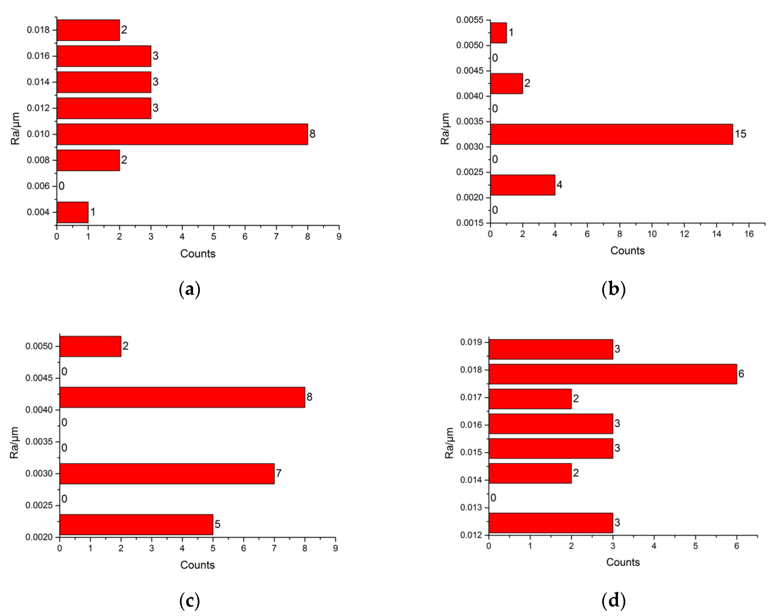
Figure 8 shows the best surface morphology of each sample. The optimum surface roughness of each sample is 4, 2, 2, and 12 nm respectively with all selected length 42 μm. The results show that the etched regions of sample 2 and 3 have the best surface morphology, while sample 4 has the worst profile.
Table 2 lists the roughness distribution of 22 test groups of each sample, and Figure 9 shows the surface roughness distribution in different areas of each sample. From figures we can see that sample two and three have the best surface morphology and its roughness mostly lies in 2–4 nm, the standard deviations are also minimal, less than 1 nm. However, the surface morphology of sample four changes little, most of which remained between 12–21 nm, but its average roughness is the largest. The largest fluctuating surface morphology is sample one, which has the maximum standard deviation 3.38 nm with roughness as low as 4 nm and roughness as large as 56 nm.
4. Conclusions
Silicon optical waveguides has been successfully prepared by electron beam exposure and reactive ion etching, and the production process and parameters are introduced in detail. The boundary tracing method is used to extract the data of the two-dimensional boundary of the silicon optical waveguide before and after RIE. According to the extracted data, the roughness values of the sidewall profile with different relevant lengths are calculated. The results show that the side wall roughness does not change significantly with the relevant length, most of which are controlled within 10nm before RIE, and the maximum is no more than 23 nm after RIE. Then, CLSM is used to directly measure the roughness of the bottom of waveguide etching, and the results show that more than half of the roughness of the bottom is controlled within 20 nm. Some has a relatively uniform surface with large surface roughness, which may be caused by impurities on the surface of the sample.
Author Contributions
Conceptualization, Y.Z.; Methodology, Y.Z.; Investigation, P.G., X.K. and L.J.; Data Curation, X.K. and P.G.; Writing—original draft preparation, P.G.; Writing—review and editing, P.G. and Y.Z.; Funding Acquisition, Y.Z. and J.D.; All authors analyzed the data, contributed to scientific discussion.
Funding
Supported by the National Key Research and Development Program of China (No. 2017YFB1104800), the National Natural Science Foundation of China (No. 51475479), the Key Research and Development Program of Hunan Province, China (No. 2016GK2098), the State Key Laboratory of High Performance Complex Manufacturing, Central South University (No. ZZYJKT2017-07), and the Key Laboratory for Precision & Non-traditional Machining of Ministry of Education, Dalian University of Technology (No. JMTZ201804).
Conflicts of Interest
The authors declare no conflict of interest.
References
- Meister, S.; Franke, B.; Eichler, H.J.; Kupijai, S.; Rhee, H.; Al-Saadi, A.W.S.; Zimmermann, L. Photonic Integrated Circuits for Optical Communication. Opt. Photonik 2012, 7, 59–62. [Google Scholar] [CrossRef] [Green Version]
- Doerr, C. Silicon photonic integration in telecommunications. Front. Phys. 2015, 3, 137–179. [Google Scholar] [CrossRef]
- Vahala, K.J. Optical microcavities. Nature 2003, 424, 839. [Google Scholar] [CrossRef] [PubMed]
- Chen, X.; Li, C.; Tsang, H.K. Device engineering for silicon photonics. NPG Asia Mater. 2011, 3, 34–40. [Google Scholar] [CrossRef] [Green Version]
- Dai, D.; Bauters, J.; Bowers, J.E. Passive technologies for future large-scale photonic integrated circuits on silicon: Polarization handling, light non-reciprocity and loss reduction. Light Sci. Appl. 2012, 1, 500–505. [Google Scholar] [CrossRef]
- Rahman, M.S.B.A.; Ater, F.S.S.; Mohammad, R. Effects of random sidewall roughness on optical power splitter. Opt. Eng. 2015, 54, 055103. [Google Scholar] [CrossRef]
- Barwicz, T.; Haus, H.A. Three-Dimensional Analysis of Scattering Losses Due to Sidewall Roughness in Microphotonic Waveguides. J. Lightwave Technol. 2005, 23, 2719–2732. [Google Scholar] [CrossRef]
- Gnan, M.; Thoms, S.; Macintyre, D.S.; De La Rue, R.M.; Sorel, M. Fabrication of low-loss photonic wires in silicon-on-insulator using hydrogen silsesquioxane electron-beam resist. Electron. Lett. 2008, 44, 115. [Google Scholar] [CrossRef]
- Lee, K.K.; Lim, D.R.; Kimerling, L.C.; Shin, J.; Cerrina, F. Fabrication of ultralow-loss Si/SiO2 waveguides by roughness reduction. Opt. Lett. 2001, 26, 1888–1890. [Google Scholar] [CrossRef]
- Binnig, G.; Rohrer, H.; Gerber, C.; Weibel, E. Surface studies by scanning tunneling microscopy. Phys. Rev. Lett. 1982, 49, 57–61. [Google Scholar] [CrossRef]
- Jang, J.H.; Zhao, W.; Bae, J.W.; Selvanathan, D.; Rommel, S.L.; Adesida, I.; Abeles, J.H. Direct measurement of nanoscale sidewall roughness of optical waveguides using an atomic force microscope. Appl. Phys. Lett. 2003, 83, 4116. [Google Scholar] [CrossRef]
- Martin, Y.; Wickramasinghe, H.K. Method for imaging sidewalls by atomic force microscopy. Appl. Phys. Lett. 1994, 64, 2498–2500. [Google Scholar] [CrossRef]
- Hosomi, K.; Shirai, M.; Hiruma, K.; Shigeta, J.; Katsuyama, T. AFM characterization of GaAs/AlGaAs waveguides. IEICE Trans. Electron. 1996, 79, 1579–1585. [Google Scholar]
- Sum, T.C.; Bettiol, A.A.; Seng, H.L.; Kan, J.V.; Watt, F. Direct measurement of proton-beam-written polymer optical waveguide sidewall morphorlogy using an atomic force microscope. Appl. Phys. Lett. 2004, 85, 1398–1400. [Google Scholar] [CrossRef] [Green Version]
- Pandraud, G.; Margallobalbas, E.; Yang, C.K.; French, P.J. experimental characterization of roughness induced scattering losses in PECVD SiC waveguides. J. Lightwave Technol. 2011, 29, 744–749. [Google Scholar] [CrossRef]
- Pani, S.K.; Wong, C.C.; Sudharsanam, K.; Lim, V. Direct measurement of sidewall roughness of polymeric optical waveguides. Appl. Surf. Sci. 2005, 239, 445–450. [Google Scholar] [CrossRef]
- Gonzalez, R.C.; Woods, R.E.; Eddins, S.L. Digital Image Processing Using MATLAB; Prentice-Hall: Upper Saddle River, NJ, USA, 2003. [Google Scholar]
- Zhang, H.; Li, T.; Jian, A.; Sang, S.; Xue, C.; Zhang, W. Modeling and simulation of the effect of surface roughness on properties of silicon-on-insulator optical ring resonator coupled with a straight waveguide. Opt. Eng. 2015, 54, 125101. [Google Scholar] [CrossRef]
- Sparacin, D.K.; Spector, S.J.; Kimerling, L.C. Silicon waveguide sidewall smoothing by wet chemical oxidation. J. Lightwave Technol. 2005, 23, 2455–2461. [Google Scholar] [CrossRef]
- Shi, Z.; Shao, S.; Wang, Y. Improved the surface roughness of silicon nanophotonic devices by thermal oxidation method. J. Phys. Conf. Ser. 2011, 276, 012087. [Google Scholar] [CrossRef]
- Kuribayashi, H.; Gotoh, M.; Hiruta, R. Observation of Si(1 0 0) surfaces annealed in hydrogen gas ambient by scanning tunneling microscopy. Appl. Surf. Sci. 2006, 252, 5275–5278. [Google Scholar] [CrossRef]
- Armani, D.K.; Kippenberg, T.J.; Spillane, S.M. Ultra-high-Q toroid microcavity on a chip. Nature 2003, 421, 925–928. [Google Scholar] [CrossRef]
- Zhu, X.P.; Suematsu, H.; Jiang, W.; Yatsui, K.; Lei, M.K. Pulsed-ion-beam nitriding and smoothing of titanium surface in a vacuum. Appl. Phys. Lett. 2005, 87, 093111. [Google Scholar] [CrossRef]
Figure 1.
Mask design of silicon optical waveguide.

Figure 2.
Schematic diagram of waveguide manufacturing process.

Figure 3.
The boundary tracking before reactive ion etching. (a) original image; (b) binary image; and (c) application results.
Figure 3.
The boundary tracking before reactive ion etching. (a) original image; (b) binary image; and (c) application results.

Figure 4.
Roughness distribution. (a) correlation length 0.23 μm; and (b) correlation length 1 μm.

Figure 5.
The boundary tracking after reactive ion etching. (a) original image; (b) binary image; and (c) Application results.
Figure 5.
The boundary tracking after reactive ion etching. (a) original image; (b) binary image; and (c) Application results.

Figure 6.
Roughness distribution. (a) correlation length 0.23 μm; and (b) correlation length 1 μm.
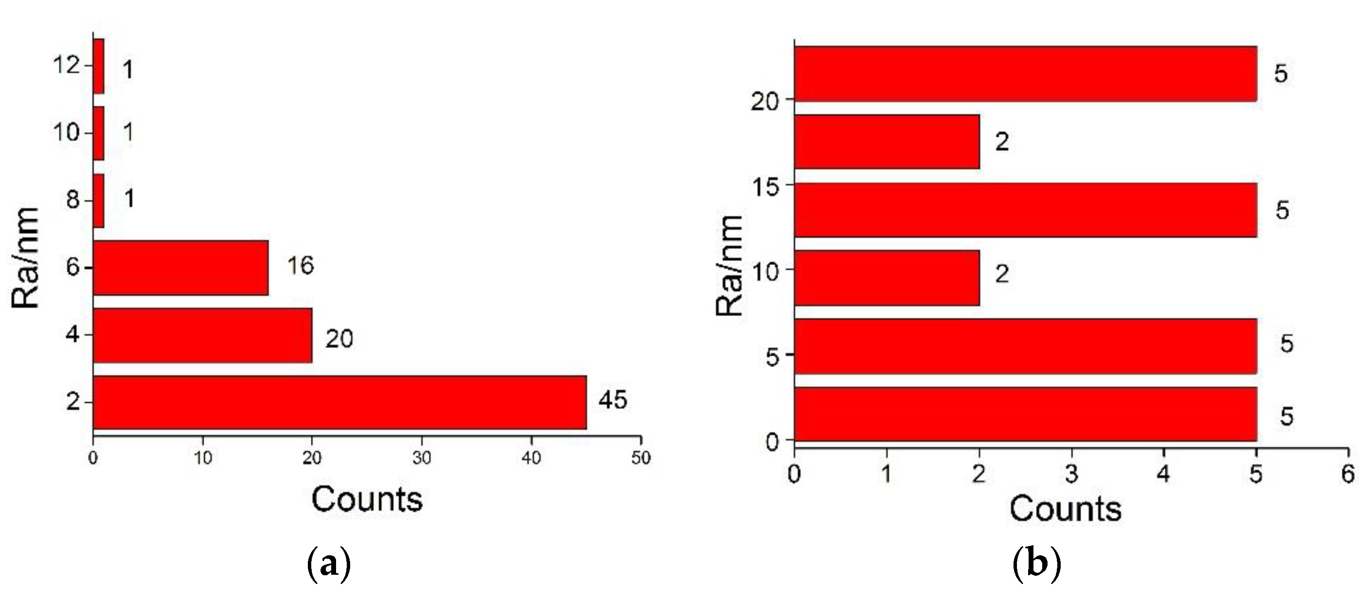
Figure 7.
3-D distribution of optimal surface morphology.

Figure 8.
Optimal surface morphology for each sample. (a) sample 1; (b) sample 2; (c) sample 3; and (d) sample 4.
Figure 8.
Optimal surface morphology for each sample. (a) sample 1; (b) sample 2; (c) sample 3; and (d) sample 4.

Figure 9.
Roughness distribution. (a) sample 1; (b) sample 2; (c) sample 3; and (d) sample 4.

Table 1.
Electron beam lithography and reactive ion etching process parameters.
| EBL Parameters | RIE Parameters | ||
|---|---|---|---|
| Sample dimension | 15 mm by 15 mm | RF power | 100 W |
| Photoresist | Thickness: 400 nm | SF6 flux | 36 sccm |
| Acceleration voltage | 50 keV | O2 flux | 6 sccm |
| Exposure dose | 300 μ C/cm2 | Gas pressure | 25 Pa |
| development | 4 methyl 2-pentanone soak for 100 s | Temperature | 25 °C |
| fixation | Isopropyl alcohol soak for 30 s | DC bias | 50 V |
Table 2.
Roughness parameters with 22 test groups of each sample.
| Roughness (nm) | ||||
|---|---|---|---|---|
| Average | Maximum | Minimum | Standard Deviation | |
| Sample 1 | 11.55 | 18 | 4 | 3.38 |
| Sample 2 | 3 | 5 | 2 | 0.69 |
| Sample 3 | 3.32 | 5 | 2 | 0.945 |
| Sample 4 | 16.18 | 19 | 12 | 2.3 |
© 2019 by the authors. Licensee MDPI, Basel, Switzerland. This article is an open access article distributed under the terms and conditions of the Creative Commons Attribution (CC BY) license (http://creativecommons.org/licenses/by/4.0/).
Share and Cite
MDPI and ACS Style
Zheng, Y.; Gao, P.; Jiang, L.; Kai, X.; Duan, J. Surface Morphology of Silicon Waveguide after Reactive Ion Etching (RIE). Coatings 2019, 9, 478. https://doi.org/10.3390/coatings9080478
AMA Style
Zheng Y, Gao P, Jiang L, Kai X, Duan J. Surface Morphology of Silicon Waveguide after Reactive Ion Etching (RIE). Coatings. 2019; 9(8):478. https://doi.org/10.3390/coatings9080478
Chicago/Turabian StyleZheng, Yu, Piaopiao Gao, Lianqiong Jiang, Xiaochao Kai, and Ji’an Duan. 2019. "Surface Morphology of Silicon Waveguide after Reactive Ion Etching (RIE)" Coatings 9, no. 8: 478. https://doi.org/10.3390/coatings9080478
Note that from the first issue of 2016, this journal uses article numbers instead of page numbers. See further details here.