Design and Manufacture of a Novel Sunlight Guiding Panel

Department of Mechanical Engineering, National United University, Miaoli 36003, Taiwan
*
Author to whom correspondence should be addressed.
Coatings 2019, 9(9), 562; https://doi.org/10.3390/coatings9090562
Submission received: 1 August 2019
/
Revised: 27 August 2019
/
Accepted: 28 August 2019
/
Published: 3 September 2019
(This article belongs to the Special Issue Design, Manufacturing and Measurement of Optical Film Coatings)
Abstract
:With technological advancement, energy consumption and lack of energy supply are inevitable. Approximately 20% of total energy consumption is used for artificial light in standard office buildings. To reduce energy consumption for illumination purposes, a sunlight guiding panel was used to increase the amount of sunlight available indoors. However, in most designs of a sunlight guiding panel, the panel has to be placed on the outdoor surface of a window glass. This type of design is inconvenient for assembling and cleaning. To enhance the practicality of a sunlight guiding panel, we attempted to place the sunlight guiding panel on the indoor surface of a window glass. The simulation results revealed that when the sunlight guiding panel was placed on the indoor surface of a window glass, the aspect ratio of the light-guiding structure of the sunlight guiding panel had to be increased for guiding the sunlight from outdoors so as to increase the amount of sunlight indoors. To fabricate the proposed sunlight guiding panel, UV nanoimprint lithography was applied to pattern the light-guiding structure of the sunlight guiding panel. Moreover, a mold with a high-precision light-guiding structure was used in UV nanoimprint lithography. The mold was fabricated using ultraprecision machining technology. Both analytical and experimental investigations were conducted to confirm the proposed design. The average light-guiding efficiency was 89.9% with a solar elevation angle range of 35° to 65°, and the experimental results agreed well with the simulation results. This study elucidates light-guiding efficiency when the sunlight guiding panel is placed on the indoor surface of a window glass, which can increase the usage convenience and application potential of sunlight guiding panels.
1. Introduction
With advancement in technology, energy consumption and lack in energy supply are inevitable. In 2015, the energy consumption for lighting in various types of buildings in Taiwan was 10%–30% of the total energy consumed, as shown in Figure 1 [1]. Figure 2 presents the statistical results of energy consumption by each electrical device in the buildings presented in Figure 1. We can clearly see that the energy used for artificial light is approximately 18.8% of the total energy consumed. In recent years, to reduce energy consumption and greenhouse gas emissions, various scholars have been striving to propose developments in two following directions: The development of energy-conserving light sources [2,3] and the effective use of sunlight for indoor lighting [4,5,6,7,8,9]. Sunlight is an essential resource for illumination and is unlikely to run out in the foreseeable future. Thus, sunlight guiding systems have the potential to be developed for conserving energy.
Conventional sunlight guiding systems include applying a flat panel [4,5,6], prismatic refractors [7], and a sunlight guiding panel [8,9]. The three systems are based on the properties of light refraction and reflection. Comparing the three systems, the sunlight guiding panel has the advantages of low cost and low volume. However, in the sunlight guiding panel device, a change in the path of sunlight is based on a microscale or nanoscale light guide structure. Thus, a reliable micromachining or nanomachining technique is required for manufacturing a sunlight guiding panel. Due to the difficulty in producing a sunlight guiding panel, a sunlight guiding panel has to be placed on the outdoor surface of a window glass in most designs of sunlight guiding panels [8,9]. This type of design is inconvenient for assembling and cleaning.
Among the conventional microprocessing or nanoprocessing technologies, nanoimprint lithography [10] has the advantages of high throughput and high-precision dimension control. Note that UV nanoimprint lithography has the excellent advantage of high-throughput efficiency because no heating and cooling processes are required and because of the minimal deformation of the imprint patterns realized using thermal expansion and contraction [11]. However, a mold with a pattern of the light-guiding structure has to be fabricated using nanoimprint lithography for manufacturing a light-guiding structure. To obtain a high-quality sunlight guiding panel, high-precision mold processing technology has to be considered for the fabrication of the patterns of the light-guiding structure. Moreover, various materials have been applied to fabricate the molds, such as silicon, silicon oxide, silicon nitride, nickel, and diamond [12].
The reliable technologies for fabricating the mold used in imprinting process that have been developed so far include e-beam lithography [10,13], LIGA (German Acronym for Lithografie, Galvanoformung, Abformung) and LIGA-like processes [14], and ultraprecision machining technology [15]. In ultraprecision machining technology, the machining profile of the ultraprecision machining technology is controlled via the relative motion of the cutting tool and the workpiece or the shape of a tool tip. As the ultraprecision machining technology advances, formability and product accuracy have greatly improved. The processing feature size and machining surface roughness in ultraprecision machining technology was confirmed to be better than 100 and 10 nm, respectively [16,17]. Based on the machinable features, dimensions, and precision of the ultraprecision machining technology, the technology is suitable for manufacturing light-guiding structures of a sunlight guiding panel. The aim of this study is to develop a novel sunlight guiding panel, which can be placed on the indoor surface of window glass. The production of the sunlight guiding panel will be implemented through nanoimprint technology and ultraprecision machining technology.
2. Principle and Method
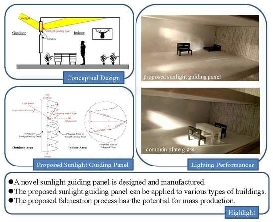
In this study, a novel sunlight guiding panel was proposed. Figure 3 displays the conceptual design of the proposed sunlight guiding panel. To enhance the practicality of the sunlight guiding panel, we attempted to place the panel on the indoor surface of a window glass. Figure 4 displays the feature of the proposed sunlight guiding panel and the predicted optical path of sunlight. Figure 4a illustrates the feature of the proposed sunlight guiding panel. The panel has four structural parameters that are denoted as L1, L2, R, and θ and are used to define the sunlight guiding panel’s polygonal prism shape. L1 is the period of the polygonal prism, L2 is the horizontal length of the polygonal prism, R is the radius of the arc that comprises the main and second slopes, and θ is the main slope’s angle of inclination. Figure 4b shows the predicted optical path of sunlight that is determined by the law of reflection (θi = θr, where θi and θr are the angles of incidence and reflection, respectively) and the law of refraction (Snell’s law, ni × sin θi = nr × sin θr, where ni and nr are the indices of refraction for the medium containing the incident ray and refracted ray, respectively, and θi and θr are the angles of incidence and refraction, respectively). Thus, the polygonal prism of the sunlight guiding panel has the potential to alter the direction of incoming sunlight toward the room’s ceiling. Moreover, when the sunlight is directed to a room’s ceiling, the brightness in the core area of the room can be increased.
The polygonal prism that is periodically arranged on the surface of the sunlight guiding panel is a key component for changing the path of sunlight. The effect of the geometrical dimensions of the polygonal prism on the light-guiding efficiency was simulated using a ray-tracing technique. In this study, the Advanced Systems Analysis Program software (version 2015, ASAP, Breault Research Organization, Inc., Tucson, AZ, USA), an optical simulation software, was used to simulate the path of sunlight through the proposed guiding panel and its light-guiding efficiency. The simulation model is as described in Figure 4a. The center wavelength of the sunlight spectrum was set to 550 nm for analysis. Four structural parameters—L1, L2, R, and θ—that are presented in Figure 4a were used to define the shape of the polygonal prism and optimize light-guiding efficiency. Moreover, the refractive indices of the substrate of the sunlight guiding panel and the polygonal prism were set to 1.5 and 1.47, respectively. The refractive indices of the outdoor and indoor areas were set to 1. Based on the optical properties of sunlight, the light source was assumed to comprise parallel rays in the simulation model. Moreover, ray tracing of 1,000,000 rays [18,19] was selected to obtain accurate analysis results. The effective light for indoor lighting was determined using the outgoing angle of light through the proposed guiding panel. Based on the description in Figure 4a, the outgoing light angles between 120° and 180° are effective for indoor lighting. Moreover, the solar elevation angle varies with the time of the day. To understand the performance of the sunlight guiding panel at different times, the angle of solar elevation was varied from 20° to 80° in the simulation model.
The fabrication of the sunlight guiding panel is conducted based on the simulation analysis results. The fabrication of the sunlight guiding panel can be divided into three procedures: Cutting the pattern of the polygonal prism on the surface of the electroless nickel mold, transferring the surface pattern of the electroless nickel mold to the polydimethylsiloxane mold (PDMS), and imprinting the sunlight guiding panel through the PDMS mold, as shown in Figure 5a–c, respectively. Figure 5a displays the schematic diagram of the processing procedure of the polygonal prism pattern. The structural shape and size optimization of the polygonal prism are conducted on the surface of an electroless nickel mold through the ultraprecision machining technology. A precision end-cutting machine was used to cut the polygonal prism pattern through a single crystal diamond tool. The angle formed by the adjacent polygonal prism is shaped according to the tip profile of the single crystal diamond tool. After cutting the angle formed by the adjacent triangles, the single crystal diamond tool turns to cut the profile of the second slope. To maintain the surface quality of the polygonal prism and avoid tool wear-associated damage, the cutting depth is controlled to be <10 µm. In our study case, the fabrication of the angle between adjacent polygonal prisms was performed using 10 repetitive cuts.
After completing the fabrication of the electroless nickel mold, the pattern of the electroless nickel mold was transferred to the PDMS mold, as shown in Figure 5b. The PDMS mold was fabricated by coating a 10:1 mixture of PDMS prepolymer and curing agent (Sylgard 184, Dow Corning, Midland, MI, USA) and then curing for 72 h at a temperature of 20–25 °C. After completing the fabrication of the PDMS mold, the sunlight guiding panel was fabricated using nanoimprint lithography, as shown in Figure 5c. The PDMS mold was used to form the polygonal prism pattern of the sunlight guiding panel. Here, the imprinted material was UV glue (FL060, Everwide Chemical Co., Ltd., Taiwan), and the substrate of the sunlight guiding panel was polyethylene terephthalate (PET) thin-film.
After the completion of the fabrication of the sunlight guiding panel, an experimental measurement was conducted for verifying the simulation results. Figure 6 illustrates the optical measurement system. The system comprises of a diode laser (650 nm) as a light source, two reflecting mirrors, a diaphragm, a polarizer, a 1/4 λ wave plate, a lens, two co-axial rotation stages (SGSP-60YAW, Sigma-Koki, Tokyo, Japan), and a power detector (PD300, Ophir Optronics Ltd., Jerusalem, Israel). Here, the flat mirrors were used to adjust the ray path for obtaining a proper optical path. The polarizer and 1/4 λ wave plate were used to make the light source characteristics similar to those of sunlight. The diaphragm and lens were used to control the beam size of the light beam and improve the divergence of the light beam, respectively.
To measure the intensity of the outgoing light at different angles of solar elevation, the sunlight guiding panel and detector were fixed on the inner and outer rotation stages, respectively. The penetration spectra at different solar elevation angles were obtained by rotating the two co-axial rotation stages. The rotation of the inner rotation stage represents the variation in the solar elevation angles, and the rotation of the outside rotation stage was used to collect light intensity data at different angles of the outgoing light.
3. Optical Analysis
The analysis results of the structural optimization of the polygonal prism are presented in Figure 7, in which the horizontal axis is the solar elevation angle and the vertical axis is the light-guiding efficiency. Figure 7a shows the influence of L1 on light-guiding efficiency of the sunlight guiding panel. L1 was varied from 50 to 60 μm. L2, R, and θ are fixed at 60, 160 μm, and 83°, respectively. The results revealed that L1 values of 50 and 55 μm exhibited a better light-guiding efficiency than L1 values of 60 μm. We attempted to further compare the cases with L1 values of 50 and 55 μm, although the L1 value of 55 μm had a better light-guiding efficiency in the solar elevation angle range of 50° to 60°, the L1 value of 50 μm had a relatively uniform light-guiding efficiency in the solar elevation angle range of 20° to 80°. Thus, a L1 value of approximately 50 µm was selected for the experimental study.
Figure 7b presents the influence of the L2 length of the sunlight guiding panel on light-guiding efficiency. The length of L2 varies from 50 to 70 µm. L1, R, and θ are fixed at 55, 160 μm, and 83°, respectively. The results revealed that an increase in L2 resulted in an increase in the light-guiding efficiency. Moreover, in this study, the pattern of the polygonal prism on the electroless nickel mold was manufactured using the ultraprecision machining technology. Based on the processing mechanism, an increase in the cutting depth may reduce the cutting accuracy and surface quality, and the aspect ratio of the cutting trench should not exceed 2. Thus, a L2 value of approximately 70 µm was selected for the experimental study.
Figure 7c presents the influence of R of the light guiding panel on light-guiding efficiency. R was varied from 140 to 180 μm. L1, L2, and θ are fixed at 55, 60 μm, and 83°, respectively. The cases with R values of 160 and 180 µm exhibited a similar spectra for the analyzed solar elevation angles, and the light-guiding efficiencies in these cases was better than that in the case with a R value of 140 µm. Moreover, by analyzing the different cases, it was found that the case with a R value of 180 µm exhibited the best light-guiding efficiency with solar elevation angles between 50° and 60°. Based on the above analysis results and discussion, a R value of approximately 180 µm was selected for the experimental study.
Figure 7d presents the influence of θ of the light-guiding panel’s light-guiding efficiency. θ was varied from 79 to 87°. L1, L2, and R are fixed at 55, 60, and 160 μm, respectively. A solar elevation angle that can cause the best light-guiding efficiency is highly affected by θ. A lower θ value results in a lower solar elevation angle with the best light-guiding efficiency. The best light-guiding efficiencies were 96%, 95%, and 89%, when θ was set to 79°, 83°, and 87°, respectively. However, in the solar elevation angle range of 20° to 80°, the overall light-guiding efficiency at 83° was slightly better than that at 79°. Thus, the θ value of 83° was proposed for experimental study.
Figure 8 shows the light-guiding efficiency of the proposed sunlight guiding panel after structural optimization. Here, L1, L2, R, and θ were 50, 70, 180 μm, and 83°, respectively. The proposed sunlight guiding panel can maintain a light-guiding efficiency >60% in a solar elevation angle range of 35° to 65°. The average light-guiding efficiency was 68% in a solar elevation angle range of 20° to 80°. The simulation results confirmed the feasibility of placing the sunlight panel on the indoor surface of a window glass. However, the aspect ratio of the polygonal prism of the sunlight guiding panel was 1.4, which is very higher than that of the sunlight guiding panel installed outdoors (e.g., the aspect ratio is 1 in reference [8]). The manufacturing of the proposed sunlight guiding panel is more difficult than previous designs.
4. Experimental Results and Discussion
4.1. Electroless Nickel Mold Fabrication
The picture and scanning electron microscope (SEM) images of the electroless nickel mold are shown in Figure 9. As shown in Figure 9a, the area of the machined surface was approximately 10 mm × 20 mm. Figure 9b displays the top view of the SEM image, whereas Figure 9c presents its cross-sectional view. According to SEM observation, the shape of each polygonal prism in the electroless nickel mold was extremely consistent, as shown in Figure 9b,c. L1, L2, R, and θ of the cut polygonal prism were approximately 49.4, 72.9, 316.5 µm, and 86.6°, respectively. The measured values of L1 and L2 agreed well with the results of the simulation’s optimization. However, a difference of approximately 3.6° was noted between the angles of θ in the experimentation and the simulation’s optimization. The difference was caused by the tip profile of the single crystal diamond tool. It must be mentioned that there was a significant difference between the size of R obtained from the experimentation and the simulation optimization. This difference was caused by the insufficient cutting depth and rotation angle of the diamond tool in the process of cutting the second slope. Based on the geometric definition of the polygonal prism, the cutting depth and rotation angle of a diamond tool were approximately 11 µm and 8° less than the expected design, respectively.
4.2. Fabrication of the PDMS Mold
Figure 10 displays the SEM image of the surface pattern of the PDMS mold. Figure 10a,b reveals the top view and cross-sectional view of PDMS mold, respectively. The surface of the PDMS mold almost completely replicated the pattern of the electroless nickel mold because PDMS is soft and flexible, thus enabling the mold to have intimate contact with the electroless nickel mold, providing a good pattern transfer property. The negative pattern of the PDMS mold had a period of 50.4 μm, a height of 72.0 μm, a tip angle of 32.3°, and the slope’s turning angle of 12.8°.
4.3. Fabrication of the Sunlight Guiding Panel
Figure 11 shows the fabrication results of the sunlight guiding panel. Figure 11a,b reveals the top view and cross-sectional view of the sunlight guiding panel, respectively. Figure 11a shows more than 20 structures of the polygonal prisms, which could be used to prove the homogeneity of the sunlight guiding panel. Comparing Figure 11b with Figure 10b, it can be seen that the surface structure of the PDMS mold was successfully transferred to the surface of the sunlight guiding panel. L1, L2, R, and θ of the imprinted polygonal prism were approximately 44.5, 72.5, 343.5 µm, and 86.5°, respectively. Table 1 lists the feature size of the surface pattern of the electroless nickel mold and sunlight guiding panel. There were some differences between the sizes of the electroless nickel mold and sunlight guiding panel. This slight difference can be attributed to polymer shrinkage. The percentage of the size differences between the surface patterns of the sunlight guiding panel and electroless nickel mold was approximately from 0.1% to 10%. This percentage was calculated based on the following equation: |Ssunlight guiding panel − Selectroless nickel mold|/Selectroless nickel mold, where Ssunlight guiding panel and Selectroless nickel mold are the same feature sizes in the sunlight guiding panel and the electroless nickel mold, respectively.
4.4. Experimental Measurement
Figure 12 shows the experimental penetration spectra and compares them with the simulation penetration spectra. Here, the feature sizes of the fabricated sunlight guiding panel were used as a reference for establishing the simulation model. According to the size of the polygonal prism of the sunlight guiding panel and machining surface roughness in ultraprecision machining technology [16,17], the optical responses of refraction and reflection are much greater than scattering. Thus, the surface roughness of the polygonal prism is ignored in the ray tracing analysis. Figure 12a,b presents the spectra at solar elevation angles of 55° and 60°, respectively. The red line pertains to the analysis result obtained using the actual feature size of the polygonal prism obtained from the SEM analysis, whereas the blue line pertains to the experimental results. The light angles of the peaks in the simulation and experimental results were determined to be similar. However, a difference of approximately 1°–7.3° was noted between the angles. Possible reasons for the difference may be attributed to the measurement error of SEM and positioning error of the sunlight guiding panel in the measurement system [20]. Furthermore, the differences in the refractive index between database and reality also slightly affect the difference between simulation and experiment [20]. In addition, the difference between the spectral profile obtained from experimentation and it being obtained from the simulation needs to be discussed. The distance between the sunlight guiding panel and detector is only approximately 100 mm in the measurement system (the ideal distance should be near infinity). Thus, in the spectral scanning process, the detector could receive the optical energy from the adjacent outgoing angle of light, thus resulting in larger full width at half maximum (FWHM) of spectral peaks. This problem is inevitable and can be found in published journal articles related to sunlight guiding panel [8].
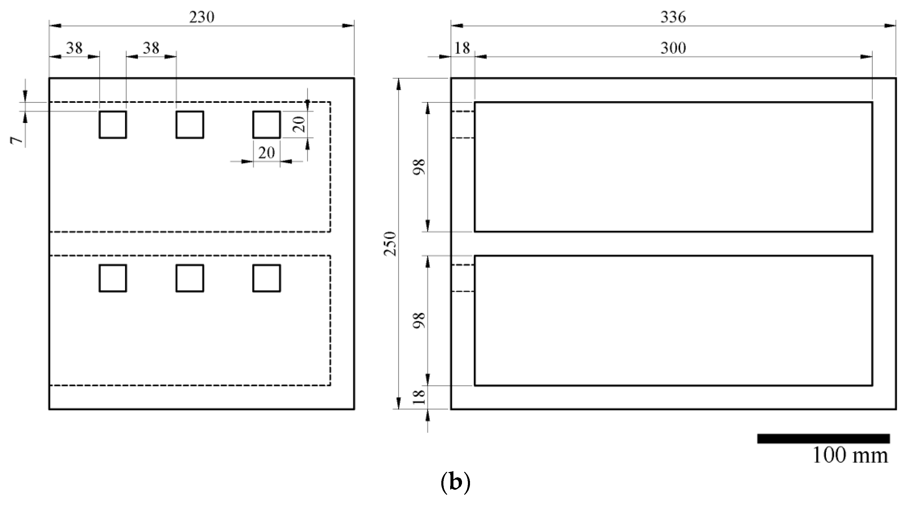
Figure 13 shows the actual use of the sunlight guiding panel in the model house. Figure 13a displays the overall appearance of the model house. Sunlight provided the light source used to confirm lighting performance. The style of the model furniture and the corresponding positions were the same in both rooms. The only difference was that the sunlight guiding panel was not used in the first-floor room and was used in the second-floor room. Figure 13b shows the floor plan of the model house used to describe the size of the model house and the position of the windows. The width, height, and depth of each room are 300, 98, and 112 mm, respectively. In addition, each room contains three windows of the same size (20 mm × 20 mm), and the distance between the windows and the room ceiling is 7 mm. Comparing the room brightness of both rooms, we can confirm that the proposed sunlight guiding panel greatly improved the brightness of the model house.
5. Conclusions
This study was dedicated to the development of a light-guiding panel that has the advantages of low production cost and an easy setting-up procedure. In design cases presented in previous studies, the sunlight guiding panel was often placed on the outdoor surface of a window glass to avoid difficulties with producing light-guiding structures. Thus, these past design are inconvenient while assembling and cleaning, and limited types of buildings can use the previously proposed designs of the sunlight guiding panel.
The simulation results revealed that the proposed light-guiding structure could maintain a light-guiding efficiency of >60% when the solar elevation angle was in the range of 35° to 65°. However, the aspect ratio of the proposed light-guiding structure was >1.4. To successfully produce the proposed light-guiding structure, ultraprecision machining technology was employed for generating the pattern of the light-guiding structure and UV namoimprint lithography was used to fabricate the sunlight guiding panel. SEM observation confirmed that the size difference between the patterns of the electroless nickel mold and replicated light-guiding structure could be <10%. Moreover, the experimental results agreed well with ASAP simulation results. This study successfully produced a novel sunlight guiding panel that could be placed on the indoor surface of a window glass. The proposed sunlight guiding panel can not only be applied to various types of buildings but also has the potential for mass production. In addition to its commercial value, the panel could effectively reduce the energy consumption of indoor lighting.
Author Contributions
Conceptualization, W.-H.H.; Methodology, W.-H.H.; Software, Y.-Z.X.; Validation, W.-H.H. and Y.-Z.X.; Formal Analysis, W.-H.H. and Y.-Z.X.; Investigation, W.-H.H. and Y.-Z.X.; Resources, W.-H.H.; Data Curation, W.-H.H.; Writing—Original Draft Preparation, W.-H.H.; Writing—Review and Editing, W.-H.H.; Visualization, W.-H.H.; Supervision, W.-H.H.; Project Administration, W.-H.H.; Funding Acquisition, W.-H.H.
Funding
This research received no external funding.
Acknowledgments
The authors are grateful to Pei-Jen Wang from National Tsing Hua University for the simulation software, ASAP. The authors also thank Hung-Yin Tsai from National Tsing Hua University for the SEM observations.
Conflicts of Interest
The authors declare no conflict of interest.
References
- Taiwan Green Productivity Foundation. Energy Audit Annual Report for Non-productive Industries 2015; Taiwan Green Productivity Foundation: Taipei, Taiwan, 2016; p. 19. [Google Scholar]
- Park, D.H.; Oh, S.T.; Lim, J.H. Development of UVB LED lighting system based on UV dose calculation algorithm to meet individual daily UV dose. Appl. Sci. 2019, 9, 2479. [Google Scholar] [CrossRef]
- Poppe, A.; Farkas, G.; Gaál, L.; Hantos, G.; Hegedüs, J.; Rencz, M. Multi-domain modelling of LEDs for supporting virtual prototyping of luminaires. Energies 2019, 12, 1909. [Google Scholar] [CrossRef]
- Edmonds, I.R.; Pearce, D.J. Enhancement of crop illuminance in high latitude greenhouses with laser-cut panel glazing. Sol. Energy 1999, 66, 255–265. [Google Scholar] [CrossRef]
- Ho, M.C.; Chiang, C.M.; Chou, P.C.; Chang, K.F.; Lee, C.Y. Optimal sun-shading design for enhanced daylight illumination of subtropical classrooms. Energy Build. 2008, 40, 1844–1855. [Google Scholar] [CrossRef]
- Park, D.; Kim, P.; Alvarenga, J.; Jin, K.; Aizenberg, J.; Bechthold, M. Dynamic daylight control system implementing thin cast arrays of polydimethylsiloxane-based millimeter-scale transparent louvers. Build. Environ. 2014, 82, 87–96. [Google Scholar] [CrossRef] [Green Version]
- Vlachokostas, A.; Madamopoulos, N. Liquid filled prismatic louver façade for enhanced daylighting in high-rise commercial buildings. Opt. Express 2015, 23, A805–A818. [Google Scholar] [CrossRef] [PubMed]
- Hocheng, H.; Huang, T.Y.; Chou, T.H.; Yang, W.H. Microstructural fabrication and design of sunlight guide panels of inorganic-organic hybrid material. Energy Build. 2011, 43, 1011–1019. [Google Scholar] [CrossRef]
- Klammt, S.; Neyer, A.; Müller, H.F.O. Redirection of sunlight by microstructured components—Simulation, fabrication and experimental results. Sol. Energy 2012, 86, 1660–1666. [Google Scholar] [CrossRef]
- Chou, S.Y.; Krauss, P.R.; Rmstrom, P.J. Imprint of sub-25 nm vias and trenches in polymers. Appl. Phys. Lett. 1995, 67, 3114–3116. [Google Scholar] [CrossRef]
- Tanabe, A.; Uehara, T.; Nagase, K.; Ikedo, H.; Hiroshiba, N.; Nakamura, T.; Nakagawa, M. Discharge of viscous UV-curable resin droplets by screen printing for UV nanoimprint lithography. Jpn. J. Appl. Phys. 2016, 55, 06GM01. [Google Scholar] [CrossRef]
- Guo, L.J. Nanoimprint lithography: Methods and material requirements. Adv. Mater. 2007, 19, 495–513. [Google Scholar] [CrossRef]
- Hsu, W.H. A method for estimating the filling rate of the mold cavity in nanoimprint lithography. J. Nanosci. Nanotechnol. 2018, 18, 4600–4606. [Google Scholar] [CrossRef] [PubMed]
- Shizuno, M.; Taniguchi, J.; Ogino, K.; Ishikawa, K. Effect of post exposure bake in inorganic electron beam resist and utilizing for nanoimprint mold. J. Nanosci. Nanotechnol. 2009, 9, 562–566. [Google Scholar] [CrossRef] [PubMed]
- Yin, S.; Jia, H.; Zhang, G.; Chen, F.; Zhu, K. Review of small aspheric glass lens molding technologies. Front. Mech. Eng. 2017, 12, 66–76. [Google Scholar] [CrossRef]
- Yuan, J.; Lyu, B.; Hang, W.; Deng, Q. Review on the progress of ultra-precision machining technologies. Front. Mech. Eng. 2017, 12, 158–180. [Google Scholar] [CrossRef]
- Zhang, Q.; Zhao, Q.; To, S.; Guo, B.; Rao, Z. Precision machining of ‘water-drop’ surface by single point diamond grinding. Precis. Eng. 2018, 51, 190–197. [Google Scholar] [CrossRef]
- Liu, Z.Y.; Liu, S.; Wang, K.; Luo, X.B. Studies on optical consistency of white LEDs affected by phosphor thickness and concentration using optical simulation. IEEE Trans. Compon. Packag. Technol. 2010, 33, 680–687. [Google Scholar] [CrossRef]
- Jung, S.M.; Kang, I.B. Three-dimensional modeling of light rays on the surface of a slanted lenticular array for autostereoscopic displays. Appl. Opt. 2013, 52, 5591–5599. [Google Scholar] [CrossRef] [PubMed]
- Hsu, W.H.; Hocheng, H.; Shy, J.T. A method for in situ measurement of residual layer thickness in nano-imprint lithography. Microelectron. Eng. 2013, 110, 132–140. [Google Scholar] [CrossRef]
Figure 1.
Analysis of the proportion of energy consumed in various types of buildings in Taiwan [1].
Figure 1.
Analysis of the proportion of energy consumed in various types of buildings in Taiwan [1].

Figure 2.
Statistical results of the energy consumption by various electrical devices in buildings.

Figure 3.
Conceptual design of the proposed sunlight guiding panel.

Figure 4.
Feature of the proposed sunlight guiding panel. (a) Structure definition method. (b) Predicted optical path for indoor lighting.
Figure 4.
Feature of the proposed sunlight guiding panel. (a) Structure definition method. (b) Predicted optical path for indoor lighting.

Figure 5.
Fabrication process of the sunlight guiding panel that include: (a) Cutting the pattern of the polygonal prism, (b) transferring the pattern to a polydimethylsiloxane (PDMS) mold, and (c) imprinting the polygonal prism of the sunlight guiding panel.
Figure 5.
Fabrication process of the sunlight guiding panel that include: (a) Cutting the pattern of the polygonal prism, (b) transferring the pattern to a polydimethylsiloxane (PDMS) mold, and (c) imprinting the polygonal prism of the sunlight guiding panel.

Figure 6.
Schematic of the measurement system.

Figure 7.
Analysis results of the structural optimization of the polygonal prism. Influence of (a) L1, (b) L2, (c) R, and (d) θ on the light-guiding efficiency of the sunlight guiding panel.
Figure 7.
Analysis results of the structural optimization of the polygonal prism. Influence of (a) L1, (b) L2, (c) R, and (d) θ on the light-guiding efficiency of the sunlight guiding panel.

Figure 8.
Light-guiding efficiency of the proposed sunlight guiding panel after structural optimization.
Figure 8.
Light-guiding efficiency of the proposed sunlight guiding panel after structural optimization.

Figure 9.
Fabrication result of the electroless nickel mold. (a) Photograph of the mold. (b) Top and (c) cross-sectional SEM views.
Figure 9.
Fabrication result of the electroless nickel mold. (a) Photograph of the mold. (b) Top and (c) cross-sectional SEM views.


Figure 10.
Fabrication result of the PDMS mold. (a) Top and (b) cross-sectional SEM views.

Figure 11.
Fabrication result of sunlight guiding panel. (a) Top and (b) cross-sectional SEM views.

Figure 12.
Comparison between the experimental and simulation results at outgoing angles of (a) 55° and (b) 60°.
Figure 12.
Comparison between the experimental and simulation results at outgoing angles of (a) 55° and (b) 60°.

Figure 13.
Model house used to confirm lighting performance: (a) Overall appearance of the model house. Here, sunlight guiding panel was not used in the first-floor room and was used in the second-floor room, and (b) floor plan of the model house.
Figure 13.
Model house used to confirm lighting performance: (a) Overall appearance of the model house. Here, sunlight guiding panel was not used in the first-floor room and was used in the second-floor room, and (b) floor plan of the model house.


Table 1.
Comparing the feature sizes of the electroless nickel mold and sunlight guiding panel.
| Features | L1 (µm) | L2 (µm) | R (µm) | θ (°) |
|---|---|---|---|---|
| Electroless Nickel Mold | 49.4 | 72.9 | 316.5 | 86.6 |
| Sunlight Guiding Panel | 44.5 | 72.5 | 343.5 | 86.5 |
| Size Differences (%) | 9.92 | 0.55 | 8.53 | 0.12 |
© 2019 by the authors. Licensee MDPI, Basel, Switzerland. This article is an open access article distributed under the terms and conditions of the Creative Commons Attribution (CC BY) license (http://creativecommons.org/licenses/by/4.0/).
Share and Cite
MDPI and ACS Style
Hsu, W.-H.; Xie, Y.-Z. Design and Manufacture of a Novel Sunlight Guiding Panel. Coatings 2019, 9, 562. https://doi.org/10.3390/coatings9090562
AMA Style
Hsu W-H, Xie Y-Z. Design and Manufacture of a Novel Sunlight Guiding Panel. Coatings. 2019; 9(9):562. https://doi.org/10.3390/coatings9090562
Chicago/Turabian StyleHsu, Wei-Hsuan, and Yi-Zhang Xie. 2019. "Design and Manufacture of a Novel Sunlight Guiding Panel" Coatings 9, no. 9: 562. https://doi.org/10.3390/coatings9090562
Note that from the first issue of 2016, this journal uses article numbers instead of page numbers. See further details here.