1. Introduction
The dynamic power consumption is represented as P ≒ αCVdd2F, where α is the probability of an output transition, C is the load capacitance, Vdd is the supply voltage, and F is the frequency of output transition. Since dynamic power is proportional to supplied voltage, lowering the Vdd voltage on selected blocks helps to significantly reduce power. Unfortunately, lowering the Vdd also increases the delay of the gates in the design.
There has been continuing development in low power technology with respect to voltage scaling. At present, many methods have been implemented, and one of the most well-known is the multi-voltage technique. Using multi-voltage circuits is an effective way to reduce power consumption. High voltage is applied to the critical function blocks or paths, while low voltage is applied to non-critical function blocks or paths. This method not only reduces power but also maintains circuit performance. The multi-voltage designed target is focused on lower power consumption under a certain performance requirement.
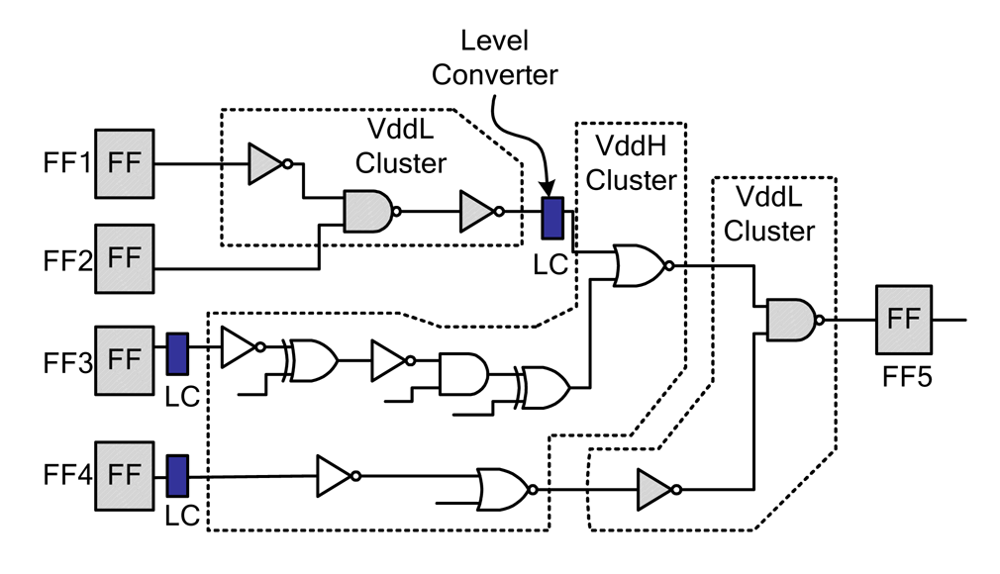
Figure 1 shows the Extended Cluster Voltage Scaling technique (ECVS) [
1]. In order not to violate the circuit delay time, the logic gates on the critical paths are assigned a higher voltage (VddH), while the logic gates on the non-critical paths are assigned a lower voltage (VddL), simultaneously. A level converter (LC) needs to be inserted into logic gates from the VddL area fanin to the logic gates in the VddH area. The voltage cluster (
VC) is a cluster of logic cell that use the same voltage; the LC is used for the low VC cells to drive the high VC cells.
The CLUSTVAR technique is an improvement from the ECVS technique. The CLUSTVAR [
2] technique combines voltage assignment with threshold voltage adjustment and gate resizing techniques to achieve significant power savings while maintaining circuit performance. It effectively utilizes the time slack to achieve the best voltage assignment to the logic gates. The ECVS and CLUSTVAR techniques are based on the voltage cluster technique and satisfy circuit performance requirements.
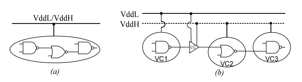
Generic low-voltage designs use one fixed voltage supply,
i.e., single Voltage Domain (VD), as shown in
Figure 2a. For ECVS cluster voltage design techniques, VddH and VddL voltage domains (
VDs) are used in the design to obtain lower power consumption. In this design, either domain can use VddH or VddL voltages.
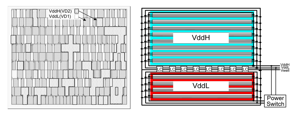
In the physical implementation of the ECVS and CLVSTVAR, both with two VD design, separate power rings are used to isolate the different supply voltage levels. The two VDs isolation design has a larger area than the single VD design. After the design phase, the LC interconnections are similarly fixed, such that the assignment of the logic gates' VDs cannot be altered, for preventing incorrect transformation of voltage levels.
The VD design of a cluster voltage technique requires that the logic cells be rearranged for grouping the same voltage gates together.
Figure 3a shows a physical placement example using the ECVS or CLUSTER technique. As in a conventional cell-based design, a different voltage level cannot apply to each logic gate in the same row. Hence, there is a concern when designing two VDs by adopting cell-based methodology. The concern is that a cell movement operation is required, which needs to collect the same VD cells together, as shown in
Figure 3b. This operation will impact the interconnection delay optimization, thereby decreasing circuit performance.
Traditional low-power design VDs are fixed when the assignment is decided after the design phase. The supplied voltage of each logic gate cannot be altered. For the proposed cell-based Voltage Domain Programmable (VDP) technique, a design method is proposed in order to reassign the voltage domains of the circuit. The whole chip VD can be flexibly programmed, for an example of two VD designs, the assignment of (VD1, VD2) can be (VddL, VddH), (VddL, VddH), (VddL, VddH), or (VddH, VddL). The assignment is based on a tradeoff of circuit power and performance. The VDP technique is different from the conventional VD technique; by using VDP, the circuit VDs are not fixed, and the assignment of logic gates can be dynamically rearranged to accommodate different voltage sources after chip fabrication.
The proposed VDP design uses multiple voltages in order to decrease power consumption while providing a power-performance tradeoff mechanism. In this VDP technique, by programming the voltage of the logic gate, designers can select different performance levels in the same design. The potential of this VDP design circuit is that the voltage domain can be switched to either a high or low voltage based on the different circuit operational modes. VDP manages power and circuit performance by using the VD reassignment technique without adjusting the clock and outer supplied voltage level.
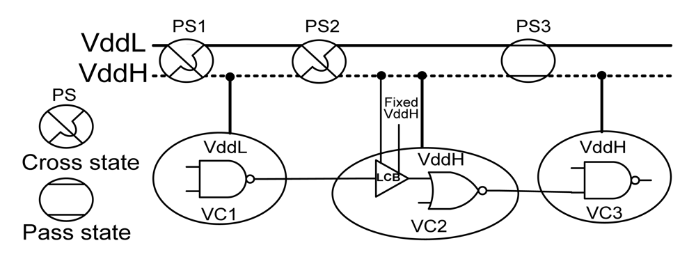
The proposed reassignment of the voltage domains of the circuit is shown in
Figure 4. In the VDP circuit, there are two power rails for each logic cell. The power switch (PS) operation is divided into two states: the cross state (
i.e., power rail cross connection) and pass state (
i.e., power rail forward connection). The level converter-buffer (LCB) is attached to the fanin logic cell to be used for the VddL gate connection to VddH gate. The PS supplies the desired voltage to each voltage cluster. For example, in
Figure 4, VC1 and VC3 use VddH, and VC2 uses VddL. As each VC can be assigned either to use VddH or VddL, the supply voltage level can be flexibly assigned. Power-performance optimization can be achieved by assigning different voltage levels to the logic gates grouped under various circuit delay time constraints. The VDP technique follows the delay time planning to increase the low-Vdd gate number count and decrease the high-Vdd logic gate number count. Hence, circuit performance and power consumption can achieve the optimal assignment.
The proposed dual suppliers VD programmable design is shown in
Figure 5. High (VddH) and low (VddL) voltage (e.g., 1.5 V and 1.2) is used simultaneously. In the conventional low-Vdd technique, the VD size is fixed, several performance-power management modes are adopted for adjusting the voltage level from two different power supplies.
The system's power consumption needs to contain the power dissipations from the design circuits and the voltage supplier (adaptor). Traditional low-power design techniques do not consider power consumption from the power supply. Only designed circuits are low power consumption and can not minimize system power utilization. Multi-Vdd is an efficient low power design technique and power sources are shared by all designed circuits. Hence, power-balance issues are becoming important for multi-Vdd complex designs. Power-balance means power utilizations from outer power suppliers are nearly equal. This can prevent the designed circuit from consuming current from one single power source, which leads to a voltage drop, degrading the circuit's performance and reliability. In this condition, the system power utilization is efficient. For example, if designed circuits A and B are both adopting VddH and VddL then low power consumptions can be achieved. The VDP provides system level power management ability to manage the logic gate quantity in A and B which utilize VddH and VddL respectively. Then, the power-balance of VddH and VddL suppliers is also achieved.
In the VDP design, the VD sizes of VddH and VddL are adjustable when the circuit changes to different operational modes. If a few gates located on the critical paths use VddH and most gates use VddL, there is lower power consumption in this VDP design. For an application example, when the VddH power source is enough (above a certain voltage level), the system operates in performance mode. When performance operational circuit quantities increase, the VddH voltage level degrades is detected by the sensor. The internal power management mechanism switches deigned circuit to low-power mode, allowing fewer gates to use VddH and more gates to use VddL, which increases the utilization balance of these two power supplies. The system level power management mechanism follows the voltage level, as measured by a built in voltage management circuit, to arrange a suitable operational mode which keeps the designed circuits functioning in the best performance-power situation.
The main idea of VDP technique is a fine-grain dual voltage scheme, in which partial gates can function at one of two different supply voltages, under operation state control signals.The contribution of this paper is broad; the VDP technique includes circuit design, CAD algorithm, and has a physical design of chip implementation and measured results. The practical application of this work is use in the power-performance manageable design. The internal voltage domain reassignment technique can replace the traditional voltage adjustment design using the voltage adaptor, and save on cost.
2. The Comparison with Voltage Scaling Techniques
Low-Vdd is an efficient technique which regulates outer supplied voltage levels to make deign circuit achieves low power consumption. As whole logic gates adopt lower voltage, the system performance is degraded.
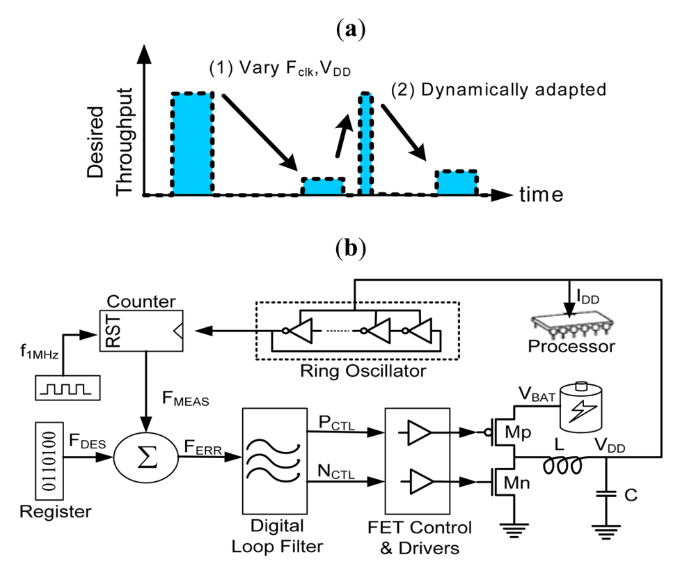
The Dynamic Voltage Frequency Scaling (DVFS) technique [
3] is an efficient low power management mechanism shown in
Figure 6, which provides for voltage and frequency adjustment that is external to the chip. This technique adjusts clock frequency and voltage in order to balance performance and power. DVFS lowers clock rates and voltages to fit the performance required by the application software. The DVFS scaling technique is based on a processor that senses its own performance level and requires a complicated voltage regulator and a frequency adaptor to control its supply voltage level and clock frequency.
As there is only one VD in the low-Vdd and DVFS design techniques, all of the logic cells in the circuit operate at the same voltage level. The supplied voltage adjusting method is applied to all of the logic gates in conventional low-Vdd and DVFS techniques. These techniques do not consider the different voltage level requirements of the logic gates within the circuit under certain delay time constraints. Hence, significant power consumption saving capability can be enhanced.
Both low-Vdd and DVFS techniques need a voltage regulator to adjust the supplied voltage level. For the power-performance management requirement, the DVFS technique is followed by the circuit performance and power consumption constraint. There are large design costs that need to be considered in order to adjust the supplied voltage and frequency to all logic gates. For a generic design, the circuit performance does not need much free adjustment. Therefore, the performance management mechanism does not require the DVFS for using a wide-range flexible adjustment voltage.
A ULS (Universal Level Shifter) circuit [
4] is presented for the static as well as dynamic power management in multi-Vdd based SoC architecture. For the requirement of dynamic power management for different voltage levels, the ULS performs three types of level converting operations (up-shifting, down-shifting, and blocking) for the input signal.
The incorporation of dual-voltage and dual-frequency for an image Discrete Cosine Transformer (DCT) is presented in [
5]. The designed architecture developed under the clock signal designed for non-DCT modules is four times faster than the clock signal for the DCT module. The DCT core modules use a lower voltage and frequency for reducing the power consumption while exploiting pipelining operations to achieve high performance.
VDP does not use an external voltage regulator, and thus requires less overhead cost. The presetting technique is simple when compared with the complex control mechanism of the DVFS. This design technique is more suitable for generic designs that do not require large flexibility in the adjustment of its circuit performance.
Compared to conventional low-Vdd and DVFS techniques, the VDP has lower power consumption than the low-Vdd technique, with more efficient power management capabilities than the DVFS technique for complex system designs (e.g., multi-core and 3D stacking designs). However, VDP follows the embedded pre-set operational modes. The adjustment flexibility is not as good as that of the low-Vdd and DVFS techniques. By using VDP technique, the two battery structure has a long operation time with low area overhead, does not require additional power management chips, and thereby decrease the total cost.
3. Voltage Domain Programming (VDP) Technique
Multi-Vdd (e.g., ECVS voltage cluster techniques) only fulfill low power consumption requirement, without considering the power management requirement. The proposed VDP technique is based on the ECVS technique. During the voltage domain programming stage, the designed circuit uses the voltage domain assignment mechanism to manage the circuit. The proposed VDP technique combines the functionalities of low-power and power-management techniques. After chip manufacturing, the VDP circuits can still be easily controlled to adjust circuit power consumption and performance according to the user/application requirement.
The VDP technique is proposed to reassign the VDs during circuit change operation mode. VddH and VddL voltages applied to logic gates are programmable, and logic gates can be specified as belonging to VddH or VddL according to the delay time constraint settings. The different VDs allow the chip performance and power consumption to be flexibly adjusted. In this VDP technique, by programming the voltage of the logic gate, designers can select different performance modes in the same design. Thus, VDP technique significantly lowers power consumption while providing dynamic power-performance management ability.
VDP switch logic gates utilize VddH or VddL dynamically during circuit operation. Hence, from adjusting the supplied voltages to the designed circuits, the complex designs can obtain good power-balance with power utilization. This system level method allows better management of power and performance of the designed system.
VDP has a quick manageable response time, and is suitable for performance adjustable design. In this paper, the design has three different implementations of the same circuit at three performance requirements, and the adjustment mechanism can be made off-line or dynamically at run-time.
The VDP technique allows VDs to be programmable in cell-based design methodology. Hence, the mixed VDs design shown in
Figure 3(a) becomes feasible. In the VDP technique, the circuit is divided into several VDs, and each VD is managed by VddH and VddL power switches. When the chip is set to different delay time constraints (operation modes), the power switches can be switched to suitable voltage sources through regulation of the VDs of VddH and VddL.
3.1. Logic Gate Voltage Domain Assignment
With the VDP technique, the circuit operation can be divided into several modes. The modes are adopted to manage the circuit operation's speed and power expenditures. Based on the multiple delay time constraints (for different operation modes), the voltage scaling technique selects the logic gates in non-critical paths using lower voltage.
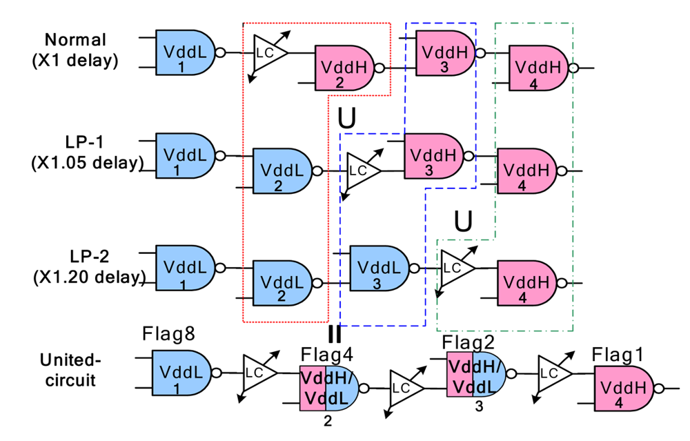
In the following circuit example shown in
Figure 7, the gates with symbols VddH and VddL denote gates that use high voltage and low voltage, respectively. In this example, the performance ×1.0 refers to the circuit's original delay time (Normal mode). ×1.05 (LP-1 mode) and ×1.2 (LP-2 mode) represent circuit delay time increases of 5% and 20%, respectively.
In the Normal (performance) mode, more gates require higher levels of supply voltage and more current consumption from the VddH. When the chip selects the LP (low-power) mode, current consumption of VddH power supplier is decreased from the few gates using the VddH, but the current consumption of VddL power supplier is increased. The VddH current values are degraded when the operation mode is switched from Normal mode to LP-1 and LP-2. However, the VddL current values are increased.
As the designed circuit has three operation modes, eight flags are assigned to logic gates after the united operation, as shown in
Table 1.For example, Flag2 (of gate-3) means that the gate connects to VddH, VddH, and VddL under the original circuit delay time multiplied by 1.0, 1.05, and 1.2, respectively. Flag4 (of gate-2) means that the gate connects to VddH, VddL, and VddL under the original circuit delay time multiplied by 1.0, 1.05, and 1.2, respectively.
By assigning the logic gates with different supply voltages, then the circuit delay time versus power consumption is manageable. For example, in the VDP circuit of
Figure 7, in the Normal mode, gate-1 uses VddL and gates-2, -3, -4 use VddH. In LP-1 mode, gate-1, and gate-2 use VddL and gate-3, and gate-4 use VddH. In LP-2 mode, gates-1, -2, -3 use VddL and gate-4 uses VddH. Hence, the VddL logic cell numbers increase when the circuit operates at lower power consumption conditions. After such assignments, gate-1 uses VddL and gate-4 uses VddH only, while gate-2, and gate-3 may use VddH or VddL, depending on operation mode.
A new level-converter-buffer (LCB) is attached to the fanin logic cell for use in the VddL gate connection to VddH gate. If the Flag assigned for a logic gate is not Flag1, this means the logic gate can be assigned to VddH or VddL, depending on the operational mode, and then LCB needs to be added to this gate output. The LCB has both level conversion and buffer functionalities, as LCB output voltage fixed VddH, the PS state change does not impact the LCB output voltage level. In each mode, different numbers of LCB and PS are required. After the circuit mode united operation, due to the need to union the LCB and PS of the three modes, the largest numbers of LCB and PS are adopted for the United-circuit. The United-circuit then unites the above three assignments and increases the three LCBs in the circuit.
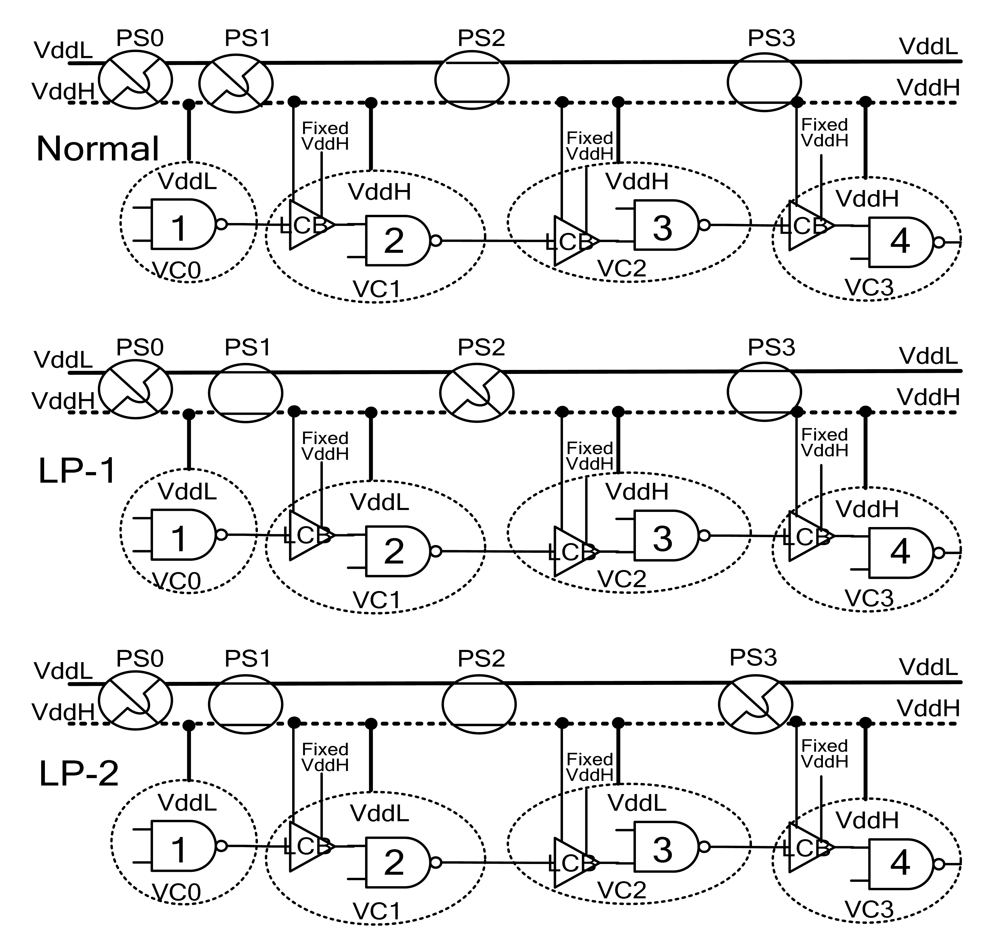
3.2. Power Switch Control State Programming
Figure 8 shows the proposed power rail circuit diagram for the United-circuit in
Figure 7. In the VDP circuit, there are two power rails for each logic cell. The PS need to provide the correct voltage level through these two power rails. The PS operation is divided into two states: the cross state (
i.e., power rail cross connection) and pass state (
i.e., power rail forward connection). The PS are well controlled to supply the desired voltage to each Voltage Cluster (VC). For example, in
Figure 8 Normal mode, VC0 uses VddL the VC1, VC2, and VC3 use VddH. The supply voltage level can be flexibly assigned.
Figure 8 shows the example of gates in the same row in three operation modes after the cell merging process. Among the three operation modes (Normal, LP-1, and LP-2), the VC1 logic cells work in the Flag4 case, and VC2 logic cells work in the Flag2 case. VC0 and VC3 logic cells work in Flag8 and Flag1 cases, respectively.
In
Figure 8, the gate flag of (gate-1, gate-2, gate-3, gate-4) equals (Flag8, Flag4, Flag2, Flag1) of the United-circuit. The Flag-4 map to PS control state 100 of gate-2 represents the supply voltages of VddH, VddL, and VddL when operating in Normal, LP-1, and LP-2 modes, respectively.
Figure 8 shows the PS states working in 3 modes. In the Flag map to PS control state, Flag = 0 denotes a PS forward-connection, and Flag = 1 denotes a PS cross connection. When the United-circuit works in LP-1 mode, the control flag of (Flag8, Flag4, Flag2, Flag1) is assigned for the (VddL, VddL, VddH, VddH) voltage to cluster (VC0, VC1, VC2, VC3). The power switch state of (PS0, PS1, PS2, PS3) equals (1, 0, 1, 0), and the power switch state equals (Cross, Pass, Cross, Pass). Then, (VC0, VC1, VC2, VC3) equals (VddL, VddL, VddH, VddH).
5. The Design Comparisons and Test Chip Validations
5.1. Comparisons with Other Multi-Vdd and Low-Vdd Techniques
Detailed comparisons between two conventional fixed voltage domain techniques are shown in
Table 2. For an 8-bit ALU test circuit,
Table 2a shows Single/Dual VD results;
Table 2b shows the results of using VDP technique. In
Table 2a,
normal refers to fixed VD by using a single supplied voltage (1.8 V or 1.2 V only).
Multi-Vdd refers to the use of two supplied voltages (1.8 V and 1.2 V both) by using a multiple voltage design tool proposed by [
2]. ×1.0, ×1.05, and ×1.2 refers to the voltage domains assigned by these related delay time constraints, which are longer circuit delay times than those of the originally designed circuit by 0%, 5% and 20%, respectively. This VDP design has 79 LCB and 63 PS. After the physical implementation, the area overhead is 5%.
Compared to the original (Normal) circuit, the ×1.0, ×1.05, and ×1.2 are extensions of the original circuit delay time for the same circuit. Three programmable voltage domains have been defined under preplan extended circuit delay times. The average power and delay time in this table uses the Normal (1.8 V) as the basis of comparison, e.g., ×1.0, ×1.05, and ×1.2 circuits resulted in 6%, 25% and 34% power reductions, respectively. The circuit delay times increase 0%,22%, and 57%, respectively.
The following experiment demonstrates the VDP design details of performance-power management ability. The delay time and power consumption are partitioned into four modes in
Figure 17. The voltage assignments are VddH = 1.8 V, and VddL = 1.8 V for the All-high mode, VddH = 1.8 V, and VddL = 1.2 V for the high performance (fast) mode and the low power modes, and VddH = 1.2 V, VddL = 1.2 V for the All-low mode. With the VDP technique, the low-power mode uses a greater number of VddL gates than does the high performance mode. From the postlayout simulation comparisons, the VDP power consumption and delay time can be graded. The simulation results show the test circuit delay time and power consumption can be clearly classified. This means that the VDP is an effective power-performance management technique.
From the power consumption and delay time comparisons, the conventional multi-Vdd technique has the lowest power-delay product. The conventional technique requires an external voltage regulator to adjust the voltage level to manage power-performance. However, the VDP technique is a single chip design, that adopts voltage domain rearrangement to manage circuit performance and power consumption with less additional area.
The VDP design technique was validated by a MPEG VLD (Variable Length Decoder) test chip.
Figure 18 shows the MPEG VLD circuit structure. The test chip has three operation modes: normal (Normal) and two low-power (LP-1, LP-2) modes. The chip's power-performance management mechanism can be implemented by controlling the circuit operation in three modes.
For the power consumption comparisons, consumed current comparisons for VddH and VddL are required. The current amount shows that the LP-2 mode uses more VddL gates than do Normal and LP-1 modes.
The current comparisons show the VddH and VddL measurement results, compared with normal mode in
Figure 19. The LP-2 mode uses fewer VddH gates and more VddL gates. There is 58.1% I
VddH reduction, and 53.2% I
VddL increase.
After the test chip physical implementation, the
output4 waveforms of the post layout simulations are shown in
Figure 20. Comparisons of the circuit delay times of the three modes were carried out. From the longest output signal (
output4), the LP-1 mode circuit delay time is 6.9% larger than that of the Normal mode. The LP-2 mode delay time is 10.7% larger than that of the Normal mode.
5.2. VLD Test Chip Implementation
The test chip has three operation modes, i.e., normal (Normal) and two low-power modes, i.e., LP-1 and LP-2. The chip's power-performance management can be implemented by controlling the circuit operation in its three modes. The three operation modes in conjunction with the external system clock are adapted synchronously in the VDP test chip. For the power consumption comparisons, the consumed currents for VddH and VddL are separately measured. In this VDP test chip, the clock tree buffers and Flip-Flops use fixed VddH.
Figure 21 shows the die photo and specifications of the MPEG VLD test chip that uses TSMC 0.18 μm CMOS technology. The chip function proof of this novel methodology to show significant decreases in power consumption and is successful in power-performance tradeoff applications.
After measurement, the observations prove that most of the logic gates use VddL in the circuit. The VddL is the dominant source of circuit power consumption and VddH is the major factor in circuit performance. When the VddL voltage level degrades, there are large power saving gains. Adjusting the VD size of VddL can play a major role in the management of circuit power consumption. However, fewer gates use VddH, which determines the circuit performance (i.e., highest operation frequency).
5.3. Chip Measurement Results
Figure 22 shows the power consumption with respect to Single-Vdd and Double-Vdd. Single-Vdd uses single voltage source (
i.e., VddH = VddL = 2.2 V). Double-Vdd uses two voltage sources (
i.e., VddH = 2.2 V and VddL = 1.6 V). The VddH and VddL connect to individual outer power supplies. Test chip power consumption is computed by (VddH × I
VddH) + (VddL × I
VddL), where I
VddH and I
VddlL are the average currents of VddH and VddL outer power supplies, respectively. The power consumption of Double-Vdd technique is reduced 55% compared to that of Single-Vdd technique. However, the highest operation frequency in Double-Vdd technique is a little lower than that of Single-Vdd technique.
Figure 23 shows the power consumptions with respect to VddH and VddL, respectively. The 蜐 symbol line shows the total power consumption for summation of the VddL and VddH power consumptions. The VddH power consumption follows the operation frequency increase. Of special note is that the power consumption of the VddL is stable and increases slowly. The circuit performance is dependent on the VddH. Most of the gates use VddL. Even at low operation frequency, the power consumption is dominated by gates using VddL. At low operation frequency, VddH consumes less current than VddL power source. When the circuit works at 70MHz, the power consumptions are nearly the same for VddH and VddL.
Figure 24 shows the performance-power management comparisons of different modes. The VddH and VddL power consumption curves of LP-2 envelop the VddH and VddL curves of LP-1. For a certain working frequency requirement, both LP-1 and LP-2 modes can be adopted (e.g., 40MHz). From the system level power management view point, the operational mode can be arranged to LP-1 or LP-2 that based on the outer supply voltage level (which power source is sufficient). As the LP-2 mode uses more VddL gates than Normal and LP-1 modes, VddL current is higher than VddH current. In LP-1 mode, the VLD circuit has higher operation frequency than in LP-2 mode. The VddH source has higher power consumption in LP-1 mode than in LP-2 mode. However, the VddL source has lower power consumption in LP-1 mode than in LP-2 mode. The power summations of VddH and VddL voltage sources are nearly the same as those of LP-1 and LP-2 modes. In the system level power management, if the VddL power loading is lighter than VddH, then the LP-2 can be adopted. The power source balance can achieve the best power utilization efficiency.
Figure 25 shows the comparisons of the test chip using different VddL in different modes. When VddH = 2.2 V is fixed and the VddL decreases from 1.7 V to 1.6 V, compare to Normal mode, the highest working frequency of LP-2 mode is lower than 9.7%, the current consumption is lower than 13.5% at 65 MHz, the performance and power consumption can be clearly differentiated. For Normal mode, fewer gates use VddL, and there is no difference in performance. The current consumption for LP-2 mode shows a reduction of 17.2%. Hence the VDP and supply voltage shrinking mechanisms can be joined together, utilized by changing operational mode to obtain lower power consumption without performance lost.
When designed circuit uses the VDP technique, the circuit performance is dependent on the VddH voltage level. High VddH allows the test chip to work at higher frequency than low VddH. Regulating VddL voltage level can play a major role in the management of the circuit power consumption. The circuit power consumption is easily degraded by lowering VddL voltage level. The circuit performances of the three operation modes can be easily classified when adjusting the VddH voltage level.
When degraded the supply voltage levels, by adapting the outer supply voltage level uses VddH = 1.8 V, VddL = 1.8 V, there is an 80% power reduction for the chip using VddH = 1.8 V, VddL = 1.2 V, shown in
Figure 26. The three modes can be easily used to manage the power consumption and performance. In
Figure 26, the LP-1 mode is taken as the comparison basis The Normal mode has 5.71% higher power consumption than LP-1 mode and LP-2 mode has 5.25% lower power consumption than LP-1 mode at VddH = 1.8 V, VddL = 1.2 V. There is an 11% power consumption interval within Normal and LP-2 modes.
In
Figure 27, in comparing maximum circuit working frequencies, Normal mode has a 15% higher working frequency than LP-1 mode, and LP-2 mode has 30% lower working frequency than LP-1 mode at VddH = 1.8 V, VddL = 1.2 V. There is 45% circuit performance interval within Normal and LP-2 modes. This figure shows circuit performance is dependent on the VddH voltage level. When degrade the VddH voltage level to 0.05 V, the performance degraded by 57% at Normal mode. Higher VddH allows the test chip to work at higher frequency than using Higher VddL.
Compared with low voltage technique at the same operation clock frequency (35MHZ), the supply voltage of VddH = VddL = 1.8 and VddH = VddL = 2.2, the low-voltage technique obtain 20% power reduction, while VDP technique has 61% power reduction.
Combining the above observations, one can elevate voltage to logic gates in the VddH voltage domain and lower the voltage to the logic gates in VddL domain. This method can achieve lowest power consumption without performance loss. This technique differs from other low voltage techniques, as it is possible to lower the supply voltage without degrading the circuit performance. Both performance and power consumption are targeted simultaneously. The process is first to choose the suitable VddH voltage for maintaining the circuit performance under specific constraints, then to degrade the VddL voltage level to achieve best performance and power saving tradeoff.
The die area is 645 × 645 um
2 for the regular VLD design without VDP technique (single voltage domain) [
6]. Compared to the single-Vdd VLD chip circuit performance, that VDP-VLD chip has no performance penalty, but requires a 46.2% large area and increased power consumption. Although from the single-chip view, there are area, power increases and PS reliability penalties. However, from the system view, manageable-power and power-balance abilities still offer greater power saving gains. Compared to the outer voltage regulation for low-Vdd and DVFS techniques, the VDP technique can be easily integrated into a single chip with less overhead.
The VDP focuses on the new embedded voltage management mechanism, which is different to the conventional techniques need to use external chip voltage adaptor. As without physical implement, the VLD chip uses conventional low-Vdd and DVFS techniques, the detailed comparisons are not taken. From the coarse comparisons, the low-Vdd and DVFS need an additional voltage adaptor to adjust the supplied voltage level, there is large cost overhead. In addition, most applications don't need dynamic and fine-scale working circuit performance. The VDP technique only changes to another operational mode with differential circuit performance and power consumption. Hence, the VDP technique is an easy method to implement a power adjustment mechanism based on the performance constraints.
There is a need to integrate the power management methods in advanced CMOS technology. Using a lower voltage is efficient method to reduce static power consumption from gate-oxide and sub-threshold leakage. As the VDP technique allows most of gate to use lower-Vdd, it can efficiently reduce static power dissipation.


