Article

Design and Analysis of Double-Gate MOSFETs for Ultra-Low Power Radio Frequency Identification (RFID): Device and Circuit Co-Design

1
VIRTUS, School of Electrical and Electronic Engineering, Nanyang Technological University, 50 Nanyang Avenue, Singapore 639798, Singapore
2
Shobhit University, Meerut 250110, Uttarpradesh, India
3
Micro Electronics and VLSI Group, Department of Electronics and Computer Engineering Indian Institute of Technology Roorkee, Roorkee 247667, Uttarakhand, India
*
Author to whom correspondence should be addressed.
J. Low Power Electron. Appl. 2011, 1(2), 277-302; https://doi.org/10.3390/jlpea1020277
Submission received: 16 May 2011 / Revised: 29 June 2011 / Accepted: 30 June 2011 / Published: 8 July 2011
(This article belongs to the Special Issue Low Power Design Methodologies and Applications)

Abstract

:
Recently, double-gate MOSFETs (DGMOSFETs) have been shown to be more optimal for ultra-low power circuit design due to the improved subthreshold slope and the reduced leakage current compared to bulk CMOS. However, DGMOSFETs for subthreshold circuit design have not been much explored in comparison to those for strong inversion-based design. In this paper, various configurations of DGMOSFETs, such as tied/independent gates and symmetric/asymmetric gate oxide thickness are explored for ultra-low power and high efficient radio frequency identification (RFID) design. Comparison of bulk CMOS with DGMOSFETs has been conducted in ultra-low power subthreshold digital logic design and rectifier design, emphasizing the scope of the nano-scale DGMOSFET technology for future ultra-low power systems. The DGMOSFET-based subthreshold logic improves energy efficiency by more than 40% compared to the bulk CMOS-based logic at 32 nm. Among the various DGMOSFET configurations for RFID rectifiers, symmetric tied-gate DGMOSFET has the best power conversion efficiency and the lowest power consumption.

1. Introduction

One of the primary motivations behind switching technology from bipolar transistors to MOSFETs is that the low power consumption of CMOS circuits along with small size makes integration possible. MOSFETs combined with technology scaling made the IC industry successful because of the reduced power, reduced area, increased speed, and low cost per chip. As the number of transistors that are integrated per chip increases, problems like leakage current, power dissipation, heat removal, cooling techniques, and reliability have been raised. These have increased the demand for power-constrained or energy-constrained design for modern VLSI systems in contrast to previous clock speed driven systems. In addition, there is an increasing class of applications like portable electronics, micro sensors, radio frequency identification (RFID), and implantable biomedical devices, which demand ultra-low power consumption and prolonged battery lifetime. All of these concerns on power reduction motivated the designers to come up with power reduction methods such as supply voltage scaling [1,2], switching activity reduction [3,4], architectural techniques of pipelining and parallelism, computer aided design (CAD) techniques for device sizing and interconnect [5,6], logic optimization [7,8], etc. Among these techniques, the most successfully proven method is the supply voltage scaling, which significantly reduces both active and static components of power. An extreme case in supply voltage scaling is the subthreshold operation where the supply voltage is less than the threshold voltage of devices. It has been proved that minimum energy per operation is achieved by operating circuits in the subthreshold region [918]. Sub-threshold circuits operate with a supply voltage that is less than the threshold of the transistors—far below traditional levels and consequently the transistors operate essentially on subthreshold current. While traditional digital logic has relied on running transistors either in the ON state (strong-inversion) or OFF state (subthreshold), sub-threshold circuits are either in an OFF state or a weak-OFF state (still in sub-threshold regime but with weak inversion). Even though subthreshold operation is limited in performance, it remains acceptable for low to medium performance and energy efficient constrained applications such as RFID, wireless micro sensors, biomedical implants, etc.
RFID tags operate in several bands—high-frequency (HF), ultra-high-frequency (UHF) and microwave bands. Transponders that operate at 125 kHz [19] and 13.56 MHz [20] have been deployed for a number of years. Their disadvantage is limited range. Passive transponders that operate in the UHF band have ranges of 7.5–9 m [21,22], and transponders that operate in the microwave band have ranges under 2 m. Karthaus et al. reported a low power RFID chip for UHF with low power consumption. This is achieved by the combination of pulse width modulation on the forward link (base-station to tag) with low RF-off times (no excess voltage droop on the on-chip power capacitor) and phase-shift keying (PSK) on the return link (tag to base-station) [22]. A high level description of a passive RFID chip that implements the EPC Class 0 protocol is provided in Glidden et al. [23]. De Vita et al. provide design criteria for the front-end of passive RFID tags [24]. While the range for passive RFID tags at UHF and microwave is adequate for some applications, greater range is strongly required. Active transponders provide greater range, but they require a battery and accordingly have a limited lifetime. Furthermore the battery should have a small form factor so that it can be seamlessly used in the assembly process for large volume production. The long lifetime (usually in excess of 10 years) and the small battery capacity require ultra-low power consumption on the active transponder to work throughout the full life of the tag.
Various research about CMOS front-ends and CMOS technology for RFID has been published [2529]. However, very few have considered double-gate MOSFETs (DGMOSFETs) for the ultra low power RFID tag design. While digital system design has continually pushed for the increased speed of minimum size devices, analog designers have often employed longer channels to avoid short channel effects (SCEs) and achieve higher voltage gain. As analog devices are scaled into the nanometer regime, CMOS technologies will require innovative device architectures and design techniques to achieve excellent analog metrics. The usefulness of nonclassical underlap channel architecture to enhance both gain and bandwidth of an OTA, alleviating gain-bandwidth trade-off associated with analog design, has been demonstrated in [30]. Kumar et al. [31] explore applications of independently driven DGMOSFETs (IDGMOSFETs) for low-power and low-voltage analog integrated circuit design. In back-gate configuration, the second gate of DGMOSFET can be used to tune the threshold voltage of the device. A simple and cascode current mirror based on bulk-driven transistor is redesigned with DGMOSFETs and shown to have smaller input voltage drop and lower power consumption. Capability of dynamic threshold tuning is exploited to design an adaptive two-stage operational amplifier (op amp) which can operate at voltages as low as 0.5 V without sacrificing performance parameters.
Freitas et al. [32] explored new capabilities brought on by IDGMOSFETs for analog baseband design. Since the two gates are disconnected, the corresponding channels are coupled resulting in a dynamic threshold voltage tuning. This operation mode is exploited to create new analog functions and low-voltage circuits. A current mirror is redesigned using IDGMOSFETs and it is shown that this structure performs an efficient differential function relating to the potentials applied to the back gates. Being adapted to low-voltage operation and self compensated from input common-mode variations, the differential current mirror is employed for the active loading of a low-voltage fully balanced OTA. Mohankumar et al. investigate the influence of both channel and gate engineering on the analog and RF performances of DGMOSFETs for system-on-chip applications [33]. The gate engineering technique used here is the dual metal gate technology, and the channel engineering technique is the conventional halo doping process.
Much work has also been done to investigate the scope of various multi-gate MOSFET structures. Several implementations of multi-gate structures include Depleted Lean-channel TrAnsistor (DELTA) [34,35], Gate-All Around device (GAA) [36], Silicon-On-Nothing (SON) MOSFET [3739], Multi-Fin XMOS (MFXMOS) [40], triangular-wire SOI MOSFET [41], n-channel SOI MOSFET [42], quadruple-gate or surrounding-gate devices having a width-to-height ratio much closer to unity [4346], quantum-wire SOI MOSFET [47,48] trigate MOSFET [49,50], CYNTHIA device (circular-section device) [51,52], pillar surrounding-gate MOSFET (square-section device) [53], planar surrounding-gate devices with square or circular cross sections [5458]. Although, theoretically surrounding gate MOSFETs might be better suited for subthreshold logic, but at the present stage of research, as per ITRS long term goals, DGMOSFETs probably will replace the existing bulk CMOS in the near future and bulk CMOS scaling trends are not even further included in the ITRS long term goals. With this view, this work focuses on DGMOSFETs for optimal ultra-low power subthreshold circuit design.
In this paper, we will explore the scope of tied/independent gates and symmetric/asymmetric gates of DGMOSFETs with circuit co-design for robust ultra-low power RFIDs. The remainder of this paper is organized as follows. Section 2 presents the background of ultra-low power RFIDs. DGMOSFETs for robust and ultra-low power subthreshold circuit design and comparison with nano-scale bulk CMOS are described in Section 3. Various DGMOSFET configurations with circuit co-design for ultra-low power subthreshold logic design are presented in Section 4. Section 5 describes the implementation of energy-efficient ultra-low power RFID rectifier circuits with various DGMOSFET configurations. Finally, conclusions are offered in Section 6.

2. Background of Ultra-Low Power RFID Design

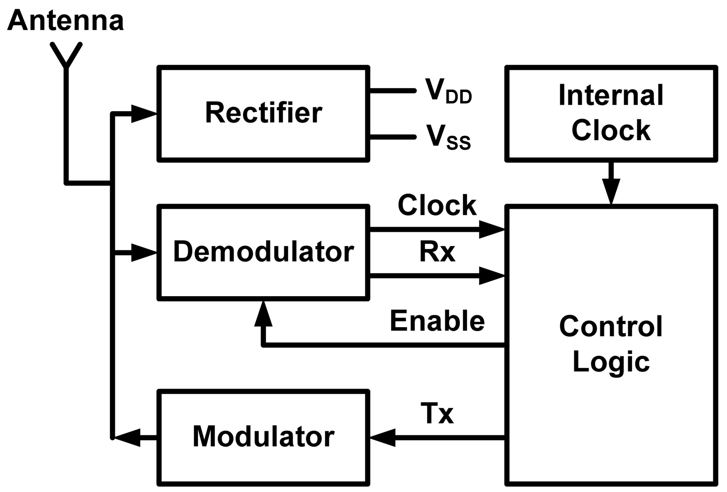
2.1. General Architecture of RFID Tag

A RFID tag is simply a transceiver (transmitter + receiver). The main difference between the RFID tag and the traditional transceivers is the passive operation, i.e., there is no battery to supply DC voltage to the chip. For this reason, a rectifier for supplying DC voltage is required. A block diagram of a RFID tag is shown in Figure 1. The rectifier block rectifies the input RF signal and generates the needed DC voltage to power the other blocks of the system. The demodulator block acts as a receiver that detects commands sent by a RFID reader. It also extracts the clock from the received RF signal, which is needed to synchronize the RFID with the RFID reader. The control logic block is the digital part of the system which controls all other blocks of the system. It determines when to receive, when to transmit and when to remain idle. It also stores the ID of the tag which is sent to the RFID reader by the modulator. The Internal clock block supplies an internally generated clock to the digital part. The modulator block acts as the transmitter of the system which sends the tag ID to the RFID reader. Decreasing the power consumption of the RFID tag is achieved generally through three ways: (a) Increasing the conversion efficiency of the rectifier, (b) Reducing the power consumption of the RFID tag blocks, and (c) Choosing a suitable communication scheme between the RFID reader and the RFID tag.

2.2. Scope of Weak or Moderate Inversion for RFID Design

The key metrics for RFID design include the transit frequency, the maximum frequency of oscillation, and the minimum noise figure. Moderate inversion or weak inversion operation offers a good trade-off between power consumption, low-voltage operation, noise, and linearity, all being of major importance for designing RFIDs. Several advantages to bias the transistor in moderate or weak inversion [18] for RFIC design are as follows.
  • Increase of the current efficiency (measured by the Gm/ID ratio) which results in a further reduction of the power consumption.
  • Decrease of the bias voltages results in lower electrical fields within the device. This avoids velocity saturation and hot electron effects. Having no velocity saturation results in transit frequency scaling as 1/L2 compared to only 1/L when velocity saturation is present. This means that scaling is more effective for devices biased in the weak and moderate inversion region than in strong inversion.
  • Having no hot electron effects avoids the increase of the noise excess factor.
  • The reduction of the bias voltages better accommodates the use of low supply voltages that are imposed by the scaling of UDSM technologies.

3. Double-Gate MOSFETs (DGMOSFETs) for Ultra-Low Power Subthreshold Circuit Design

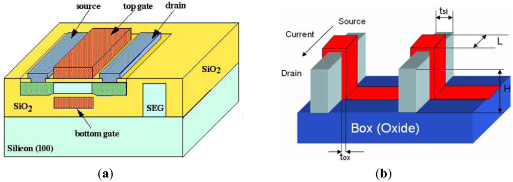
3.1. Introduction of Double-Gate MOSFETs (DGMOSFETs)

Better scalability can be achieved by introduction of a second gate at the other side of the body of each transistor resulting in a double-gate SOI structure (Figure 2a). Due to the excellent control of the short channel effects, double-gate SOI devices have emerged as the device of choice for circuit design in sub-50 nm regime [59]. Low subthreshold leakage and higher ON-current in the double-gate devices make them suitable for circuit design in sub-50 nm regime [60,61]. One of the promising structures in the double-gate technology is FinFET [62] due to the simple fabrication process (Figure 2b). Double-gate devices with isolated gates (independent gates) are being developed [63,64]. The independent gate option can be useful for low power and mixed signal applications [6469]. Such developments at the device level provide opportunities for new ways of circuit design for low power and high performance. ITRS reports also show the inevitable inclusion of DGMOSFETs in upcoming VLSI applications [69].
DGMOSFETs for optimal subthreshold operations have also been considered recently [7076]. DGMOSFETs are suitable for the sub-threshold operation due to their near ideal subthreshold slope and negligible junction capacitance. Due to the thin, fully depleted silicon body sandwiched between two gates, these devices have an excellent gate control over the channel. Furthermore, the undoped thin silicon body provides negligible source/drain p-n junction capacitance, which largely enhances the circuit performance. In general, DGMOSFETs have the following advantages over bulk CMOS technology:
  • Nearly ideal subthreshold slope.
  • Small intrinsic gate capacitance.
  • Smaller junction capacitances.
  • Better immunity to SCEs, although negligible for subthreshold operation.
  • Reduced Random dopant fluctuations (RDF) due to undoped or lightly doped body and reduced carrier mobility degradation.
  • Higher ION/IOFF ratio.
  • Design flexibility at circuit level by symmetric/asymmetric with tied and independent gate options.

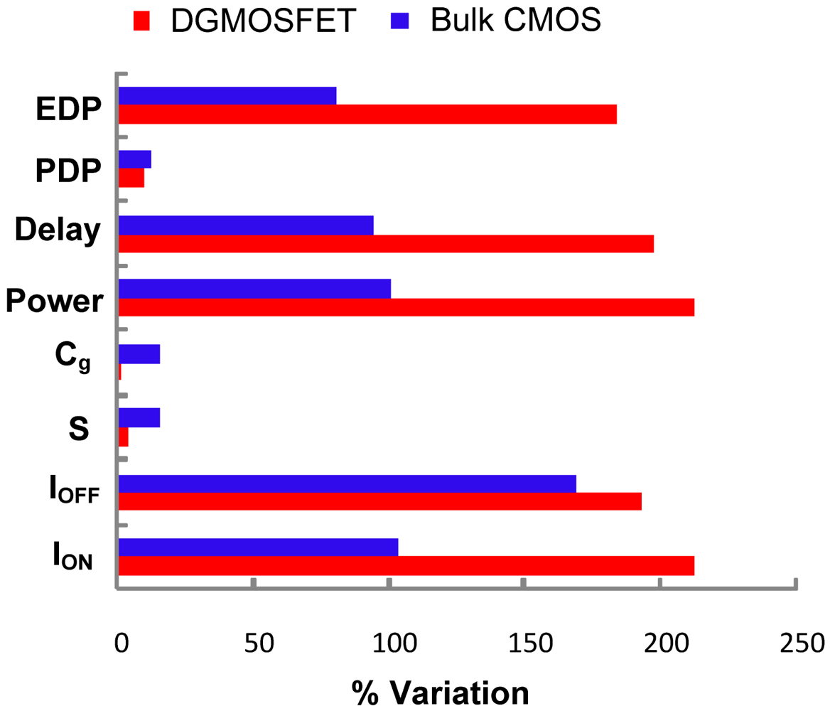
3.2. Comparison of Bulk CMOS and DGMOSFETs for Ultra-Low Power Subthreshold Circuit Design

3.2.1. Bulk CMOS and DGMOSFET Device Model Parameters

The international technology roadmap for semiconductors (ITRS), which maps out near- and long-term goals for the semiconductor industry, describes three different devices with different power delay tradeoffs: high performance, low operating power (LOP), and low standby power (LSTP). The LOP and LSTP devices are optimized in a similar manner, although the LSTP device has more stringent leakage constraints. We take bulk CMOS device parameters following [77], in which the authors follow the scaling strategy similar to that of the LSTP device. The scaling strategy is briefly described as follows: The device model has four key scaling parameters: physical gate length (Lpoly), gate-oxide thickness (Tox), substrate doping (Nsub), and peak halo doping (Np,halo). These parameters are most important when determining key device characteristics like Vth, on- current, off- current, and gate capacitance. In addition to these four parameters, Vdd is also used as an additional knob for adjusting performance. All physical dimensions other than Tox (source/drain junction depth, lateral source/drain diffusion, halo dimensions, etc.) scale in proportion to Lpoly. Lpoly is reduced by 30% per generation, which agrees well with recent Lpoly scaling trends. A survey of recent industrial publications shows that Tox has been reduced by ∼10% per generation below the 130 nm technology node [77]. In this strategy, simple assumption that Tox reduces by 10% per generation has been made. With Lpoly and Tox fixed for each generation, the remaining three parameters (Nsub, Np,halo, Vdd) may be tuned to match delay and leakage requirements. The optimization procedure uses delay (τ) as an objective and leakage (Ileak,max) as a constraint (it allows leakage to grow by 25% each generation, reduces Vdd regularly at each generation to control dynamic energy, and optimizes the device for minimum delay under the leakage constraint).
The parameter values for the NFET model at 32-nm node obtained are shown in Table 1. We have considered these device values for our simulations as they are more suitable for low power applications. As for subthreshold operation, since high performance is of secondary importance and low power is of primary concern, we considered the above-mentioned device values given in [77] at 32 nm and generated different SPICE model files for parameter variations from a specific tool called “Nano CMOS” [78] for carrying out simulations. HSPICE simulations have been carried out by setting the above device parameters for 32 nm technology in the Berkeley Predictive technology model [78] by varying different parameters and generating different SPICE model files for each set of parameters.
A compact model for DGMOSFET, akin to the BSIM model for a bulk CMOS and BSIM SOI for a SOI transistor, is not available for the purpose of circuit simulation and technology prediction. Currently, early designs with DGMOSFETs have to resort to the TCAD simulators (MEDICI, Sentaurus, ATLAS, etc.), which are computationally expensive and limit design flexibility. To overcome these barriers, an equivalent subcircuit model for a DGMOSFET device has been proposed in [79]. This circuit model consists of two fully depleted SOI devices for the front and back transistors, respectively. BSIM SOI is used as the model for each device such that this subcircuit is compatible with standard circuit simulators (e.g., SPICE). Two single-gate transistors are used to capture the current conduction controlled by the front and back gate in a DGMOSFET transistor. Each subtransistor has its own definitions of gate voltage (VG), Vth, and Tox. Their sources and drains are electrically connected to form a four-node circuit. Thus, the drain voltage (VD) and the source voltage (VS) are shared. Both subtransistors have the same gate length and width. Since the bottom of a DGMOSFET structure sits on top of a layer of SiO2, the DGMOSFET is inherently an SOI transistor. Furthermore, in the typical process range of a DGMOSFET, Tsi is so thin that the silicon body is fully depleted. Therefore, the fully depleted SOI model of BSIM (BSIM FD SOI) is used as the model basis for each subtransistor. More information about the DGFinFET device model can be found in [79].
To verify the accuracy and flexibility of predictive technology model (PTM), more than thirty sets of IV data at room temperature are collected from publications in [79]. Using the published values for technology specifications (i.e., Leff, Tox, Vth, Rdsw, and Vdd), process and physical parameters are calculated to generate corresponding PTM model files. Predicted I-V characteristics are compared to published data for verification. Even though the DGMOSFET technology is still at an early stage of technology development and thus, shows large divergence in the technology definitions, PTM is flexible enough to capture these process uncertainties. The excellent predictions prove the physicality and scalability of new PTM. HSPICE simulations have been carried out for DGSOI circuits constructed with these devices and compared with bulk CMOS circuits for subthreshold logic.

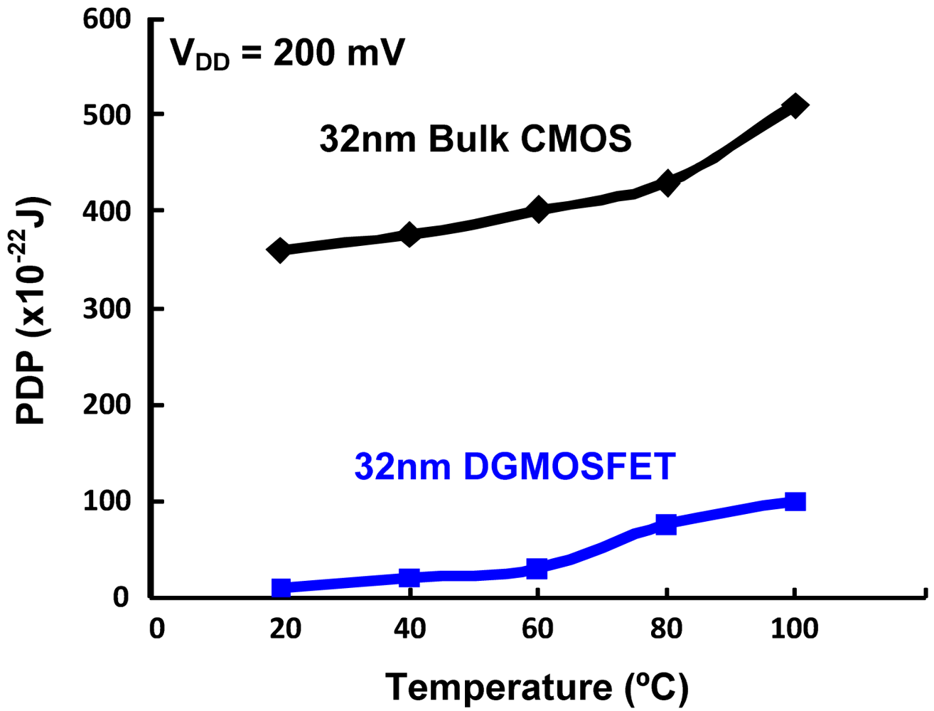
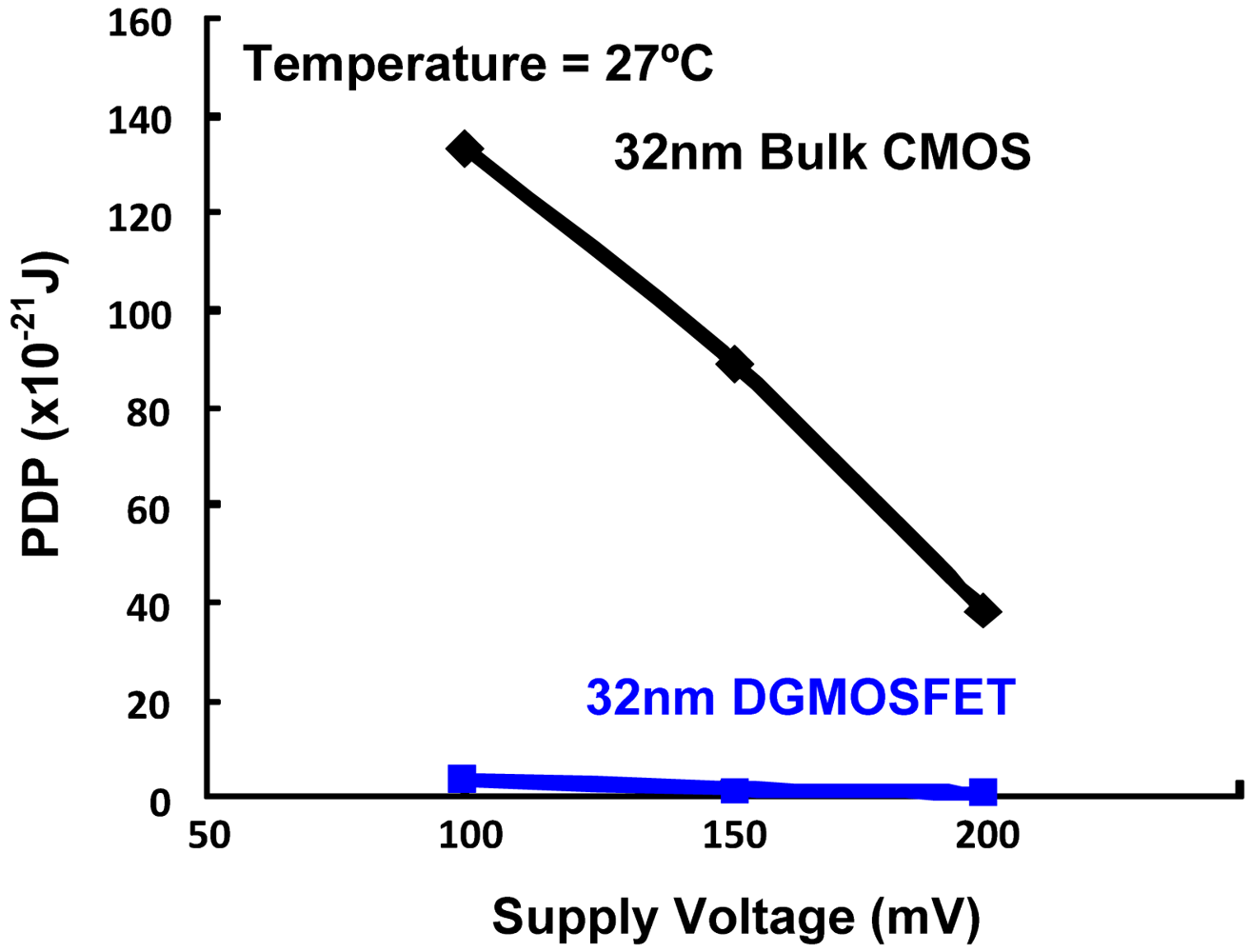
3.2.2. Comparison of Bulk CMOS and DGMOSFETs

Table 2 summarizes the performance comparisons of DGMOSFET and bulk CMOS circuits for subthreshold logic [14]. We observe that the DGMOSFET inverter power-delay-product (PDP) is approximately 70% lower than the bulk CMOS inverter and 65% lower than the pseudo NMOS inverter. Other logic gates based upon DGMOSFETs have 30–40% better energy efficiency (lower PDP) than equivalent bulk CMOS logic gates in the subthreshold operation, due to the advantages of DGMOSFETs summarized in Section 3.1. Figure 3 compares the variation in the PDP of the DGMOSFET and bulk CMOS circuits with regard to temperature, where better performance and robustness of DGMOSFET subthreshold circuits can be seen. The variation in the PDP of the DGMOSFET and bulk CMOS circuits with respect to supply voltage within the subthreshold region is illustrated in Figure 4 [14]. We also observed that a bulk MOS inverter has relatively poorer robustness in terms of noise margins and functionality compared to the equivalent DGMOSFET inverter as supply voltage scales down. It can be inferred that the suitability of DGMOSFETs for subthreshold logic compared to the bulk CMOS technology shows the possibility of scaling down of supply voltages within subthreshold region without threatening the functionality of circuits for supply voltage as low as 75–100 mV. Figure 5 summarizes the device and circuit level implications of the threshold voltage fluctuations on the bulk CMOS and DGMOSFET technologies. It can be seen that DGMOSFET is the better option for most performance metrics (almost 50% better robustness).

4. Comparison of Various DGMOSFET Configurations for Ultra-Low Power Subthreshold Circuit Design

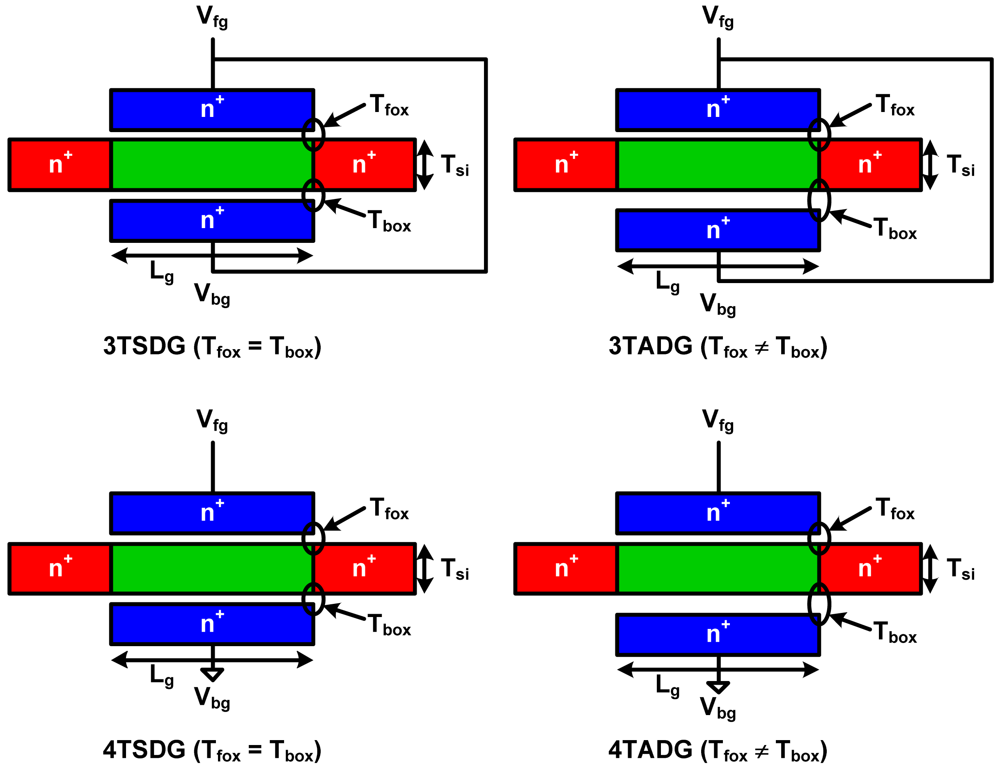
4.1. Introduction of Various DGMOSFET Configurations

DGMOSFETs can either have a three-terminal (3T) configuration, where both the gates are shorted, or a four-terminal (4T) configuration, where the back-gate bias is fixed and the front gate acts as a control electrode. If the two gates in the DGMOSFETs are tied (3T), an identical voltage can be applied to both gates. Conversely, when the two gates are independent (4T), different voltages can be applied. The asymmetry in the double gate MOSFET can be brought about by a number of ways. It can be done by applying different gate voltages to front and back gates, by assigning variation in oxide thickness to front and back gates. It can also be brought by varying gate material work functions. Independent gate technology offers an extra terminal in DGMOSFET devices at the cost of extra fabrication steps or masks. The extra feature of biasing back and front gates separately offers more flexibility and freedom to circuit designers using DGMOSFET technology. The 4T DGMOSFETs show reduced on-current along with reduced gate capacitance compared to the 3T counterparts. Moreover, 4T DGMOSFETs allow independent biasing of the two gates and offer dynamic threshold-voltage control (DTC) in circuits. Consequently, independent gate technology can be employed to help tradeoff between switching capacitance and leakage with circuit delay. Independent-gate operation benefits in circuits such as schmitt triggers, dynamic logic circuits, and sense amplifiers, and static random-access memory (SRAM) bit-cells as demonstrated recently [6972].
In this work, we will investigate four types of DGMOSFETs: tied-gate symmetric DGMOSFETs (3TSDG), tied-gate asymmetric DGMOSFETs (3TADG), independent-gate symmetric DGMOSFETs (4TSDG) and independent-gate asymmetric DGMOSFETs (4TADG) as shown in Figure 6.

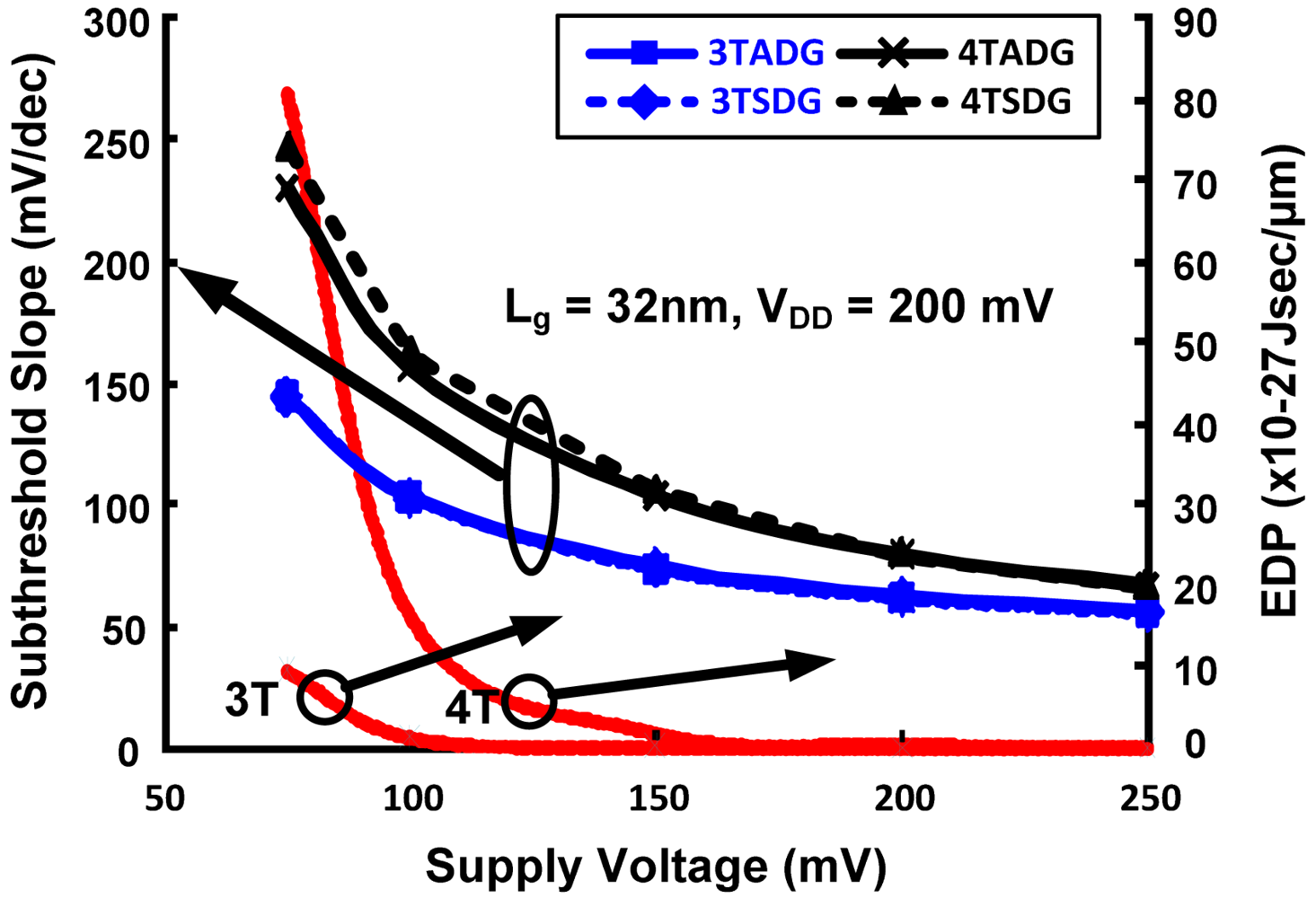
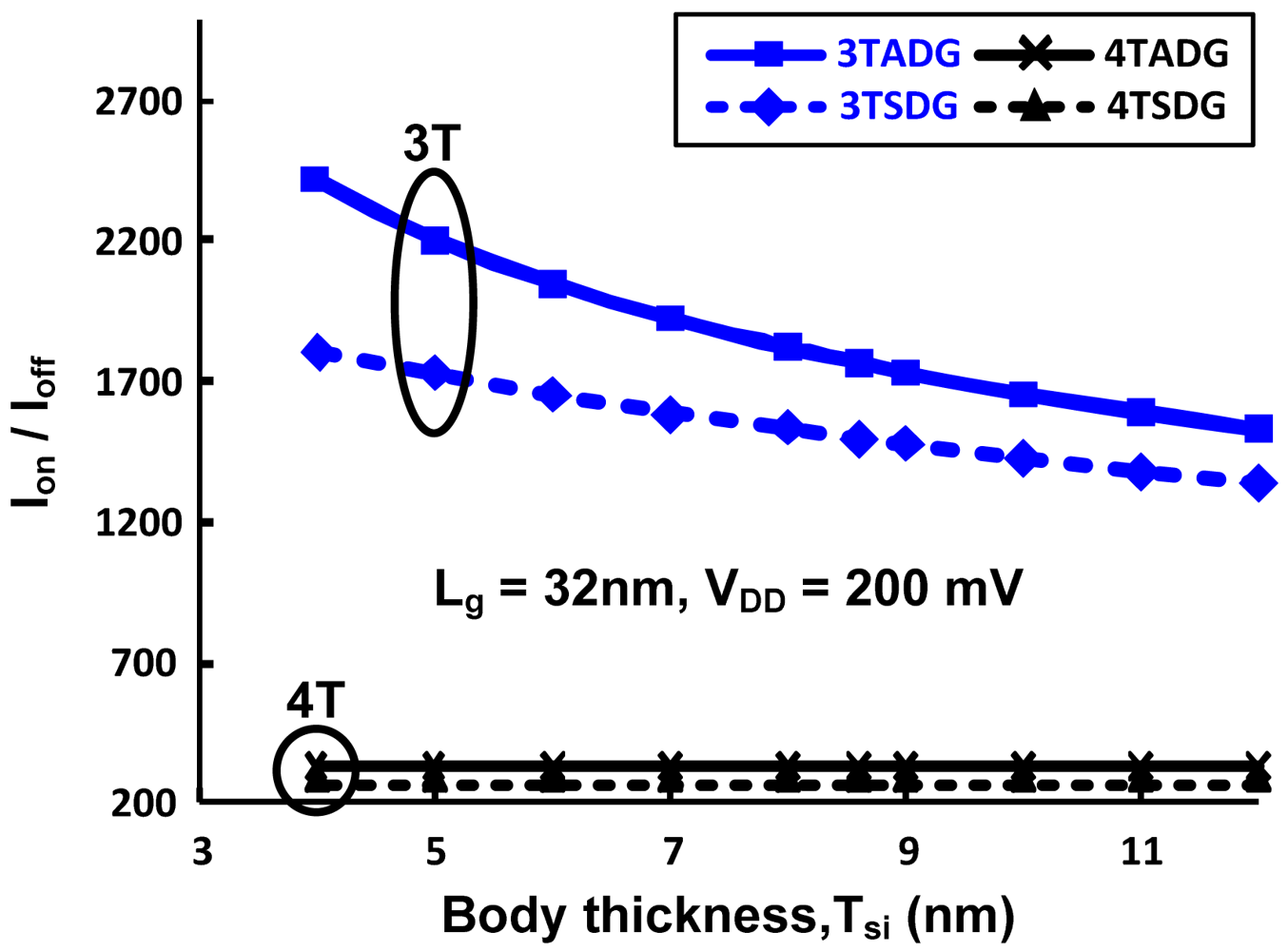
4.2. Comparison of Various DGMOSFET Configurations

HSPICE simulations have been carried out using Berkeley Predictive Technology Model (BPTM) for 32 nm DGMOSFET to study the symmetric DGMOSFETs (SDG) and asymmetric DGMOSFETs (ADG) devices and circuit performance with tied- and independent-gate options for subthreshold operation. In the following studies, we have primarily considered 4 cases: 3TSDG device (Vfg = Vbg = Vdd & Tfox = Tbox = 1.4 nm), 3TADG device (Vfg = Vbg = Vdd & TfoxTbox), 4TSDG device (Vfg = Vdd, Vbg = 0 & Tfox = Tbox = 1.4 nm), and 4TADG device (Vfg = Vdd, Vbg = 0 & TfoxTbox). The asymmetric nature of the device is being brought by taking the variation in oxide thickness for front and back gates. 3T implies that a front gate (fg) and a back gate (bg) are tied together to give the same potential while 4T implies front and back gates are applied different potentials. Device parameters extracted from the simulations are summarized in Table 3 [71]. 3TDG have better energy-delay product (EDP) performance metrics than 4TDG feature, due to the larger ION/IOFF ratio values. Asymmetric feature further enhances performance in the 3T option than in the 4T option.
Table 4 shows the comparison of 3TSDG and 3TADG performance for all basic gates and some simple combinational circuits [73]. We observe from the table that 3TADG circuits have approximately 13–14% better power consumption than 3TSDG, 4–5% better speed and 16–18.3% better PDP than 3TSDG based circuits. Table 5 shows the comparison of 4TSDG and 4TADG performance for all basic gates and some simple combinational circuits [73]. We observe from the table that 4TADG circuits only have approximately 0–0.5% better power consumption than 4TSDG, 0–1% better speed and 0.5–1% better PDP than 4TSDG based circuits. Comparison of Table 2 and 3 shows very poor power, delay and PDP performance of 4T option than 3T option for subthreshold logic, particularly as complexity of circuit increases.
Figure 7 shows the variation of ION/IOFF with body thickness for n- DG-MOSFET with different configurations in the subthreshold region of operation. From the figure it can be clearly observed that, in terms of having the highest driving capability, 3TADG is the best and 4TSDG is the worst. It is further observed that 4TSDG and 4TADG have similar pattern and better tolerance for the entire range, where as 3TSDG and 3TADG deviate more as body thickness is varied. Figure 8 shows the variation of subthreshold slope and EDP with varying supply voltage. We find 3T option having better subthreshold slope and EDP values as compared to 4T option in the entire range. Figure 9 compares the PDP variation of 3TSDG, 3TADG, 4TSDG and 4TADG devices with varying temperature in the subthreshold region of operation. Again, better robustness of 4TDG option as compared to 3TSDG and 3TADG option is observed.

4.3. Comparisons of Various DGMOSFET-Based Logic Families

In this section, we study the suitability of various logic families other than static CMOS for energy efficient subthreshold logic. NAND gates were designed with minimum sizing for functionality with various logic families and power, delay, and power delay product comparisons are done.
Table 6 summarizes the suitability of various circuit topologies for ultra-low power subthreshold operation with various configuration of DGMOSFETs [73]. For 3TSDG and 3TADG options, pseudo NMOS logic style shows to be worst in terms of power consumption and sub-CPL(complementary pass transistor logic) and sub-DCVSPG (differential cascode voltage switch pass gate) logic styles are worst in terms of delay. In terms of overall PDP, sub-CMOS shows to be the best option and sub-CPL, sub-domino and sub-DCVSL (differential cascode voltage switch logic) styles almost have a similar energy consumption. For 4TSDG option, in terms of power consumption, sub-CPL and sub-Domino logic styles shows to be better and all others have almost similar power consumption. In terms of overall PDP, sub-CMOS, sub-Domino and sub-SCVSL logic styles have almost similar and minimum energy consumption and sub-CPL and sub-DCVSPG shows to be extremely poor for 4TDG option for subthreshold logic.

5. Ultra-Low Power RFID Rectifiers with Various DGMOSFET Configurations

As the RFID tag is a passive system, DC voltage must be generated to bias the circuits of the tag, which is done by a rectifier. The rectifier converts a received RF signal into DC voltage. The main challenge in designing the RFID rectifier is to generate the required DC power using the low voltage amplitude of the RF signal with acceptable power conversion efficiency.

5.1. Various Rectifier Topologies Implemented with DGMOSFETs

5.1.1. Simple Rectifier

Power conversion efficiency (PCE) of a rectifier is defined by the output power divided by the input power. The PCE of the rectifier circuit is affected by circuit topology, diode-device parameters, input RF signal frequency and amplitude, and output loading conditions. Since the input RF signal of RFIDs in long-range operations is quite small, small turn-on voltage is the most important factor for the diode device. The Schottky diode has been utilized with a multi-stage configuration despite of the additional processing cost because of its small turn-on voltage. The rectifier circuit using the Schottky diode achieves a large PCE, but it is not compatible with the conventional CMOS technology and requires costly fabrication processing. Figure 10a shows a simple rectifier circuit implemented with 3T DGMOSFETs. Diode-connected n-channel and p-channel MOSFETs are connected in series and the internal node is connected to RF input terminal through the coupling capacitor (CC). The PCE is almost determined by the effective on-resistance of the diode-connected MOS transistor. The lower the threshold voltage of the MOS transistor is, the lower the effective on-resistance becomes. Therefore the higher PCE is obtained when the threshold voltage can be lowered. However, the threshold voltage cannot be lowered significantly since the PCE starts to be limited by the leakage current.

5.1.2. Self-Vth Cancellation (SVC) Rectifier

The PCE for a rectifier using a diode-connected MOSFET is generally worse than that of the Schottky diode due to its large threshold voltage (Vth), but when Vth cancellation techniques are utilized, the PCE can be increased dramatically. In order to reduce the effective turn-on voltage for achieving larger PCE, several Vth cancellation schemes have been proposed [8083]. One uses a switched-capacitor technique to generate DC gate bias voltage from an external power supply [80] and others generate DC gate bias voltage from the output voltage of the rectifiers themselves [8183]. Figure 10b shows self Vth cancellation (SVC) rectifier circuit implemented with 3T DGMOSFETs. It is the same as the conventional rectifier circuit described in the previous section except that gate electrodes of nMOS transistor and pMOS transistor are connected to the output terminal and ground terminal, respectively. This connection boosts gate-source voltages of nMOS and pMOS transistors as much as the output DC voltage. In other words, threshold voltages of MOS transistors are equivalently decreased by the same amount to the output DC voltage.

5.1.3. Differential Drive Rectifier

The PCE is roughly determined by the effective ON-resistance of the diode-connected MOS transistor and the minimization of the effective threshold voltage of MOS transistors results in a large PCE. However, when the effective threshold voltage of the MOS transistor is too small due to the excessive DC bias voltage, for instance, when it becomes negative, the MOS transistor is always ON and increased reverse leakage current cannot be ignored. If the reverse leakage current is not negligible, it directly results in energy loss since charges flowing in a reverse direction are simply wasted. Therefore, reverse diode loss rapidly increases. In addition, the forward current must be further increased to compensate the reverse leakage current, thus further increasing energy loss. As a result, it is concluded that we cannot achieve a small ON-resistance and a small reverse-leakage current at the same time by “static” Vth cancellation schemes. The differential drive rectifier is an “active” Vth cancellation scheme in which Vth can be minimized in a forward bias condition and be increased in a reverse bias condition automatically by a cross coupled differential circuit configuration [84]. Figure 10c shows the unit stage of the differential drive rectifier circuit with 4T DGMOSFETs and Figure 10d shows the differential drive rectifier circuit implemented with 3T DGMOSFETs.

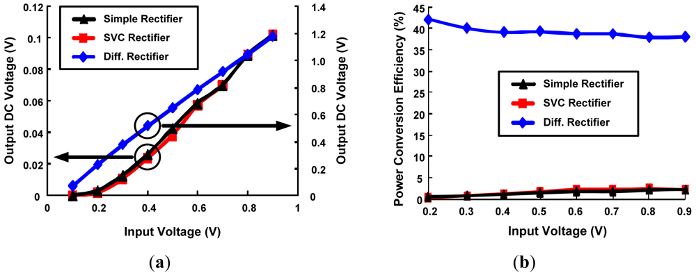
5.2. Comparison of Various RFID Rectifier Topologies Using DGMOSFETs

The above mentioned rectifier topologies are simulated using HSPICE to analyze the best topology for ultra low power RFID design with highest PCE using DGMOSFET technology. The circuit parameters are as follows: CC = CS = 10 pf and RL = 10 kΩ, W/L ratio for minimum sized devices is 2 and upsized devices is 10, Wp/Wn = 2, f = 100 MHz. Comparison of DC output voltages generated by various rectifier topologies implemented with minimum sized 3T DGMOSFETs with variation in input levels is shown in Figure 11a. Conventional and SVC rectifier topologies have almost similar and lower output voltages in comparison to higher output DC voltage generated by the differential drive rectifier. As the RF input signal amplitude change from 0.1 to 0.9 V (for a power change of 0.5–365 μw), DC output power change by 0.5–139 μw for differential drive rectifier and 1.6 pw–1 μw output power change for a SVC rectifier respectively. As a result, higher PCE values for differential drive rectifier can be seen in Figure 11b. For the same change in input voltage level, the PCE changes by 42–38% for differential drive, 0.04–2.1% for SVC and 0.2–2.1% for simple rectifier topologies. Power consumption comparison of the above rectifier topologies designed by minimum-sized 3T DGMOSFETs is described in Figure 12. SVC and conventional rectifier topologies consume lower power (0.01–36 μw for SVC, 0.01–14 μw for conventional and 0.5–515 μw for differential rectifier topologies.
RF MOS transistors are usually designed as large devices in order to achieve the desired transconductance required to meet the RF requirements. They are usually laid out as multi finger devices, because in deep submicron CMOS processes, the maximum finger length (corresponding to the unit transistor width Wf) is limited. Typical devices have up to 10 or more fingers. Here the above minimum sized devices are upsized (10 times) and simulations are carried out to see the effect of PCE and DC output power generated by the various rectifier topologies, which can be seen in Figure 13. It can be seen that for a differential drive rectifier, although the overall DC output voltage generated by upsized devices increase significantly (from 0.12–1.72 V), but the PCE will still be lower compared to minimum sized devices due to the significant increase in the input power drawn from the signal. However, for SVC and simple rectifier topologies, both the DC output power and PCE increase significantly due to the less number of devices and small input power in comparison to that of upsized differential drive rectifier topology. For SVC, DC output power rise by 91 pw–5.6μw and PCE by 0.2–4.7% and for conventional rectifier, DC output power increase by 296 pw–4.1 μw and PCE change by 1.2–2.2%. This concludes that upsizing is not beneficial for differential drive rectifier both in terms of PCE and power consumption. For SVC and simple rectifier topologies, the PCE increases in power consumption (0.04–66.4 μw for SVC and 0.03–21.2 μw for conventional rectifier).

5.3. Effect of 3T/4T, Symmetric/Asymmetric DGMOSFET Features on Differential Drive Rectifier Topology

In the previous section, various rectifier topologies comparison for 3T DGMOSFETs is done. In this section we explore more on differential drive rectifier topology. Compariosn of DC output voltages generated by differential drive rectifier topoplogy implemented with minimum and upsized 3T/4T DG MOSFETs with variation in RF input levels is presented in Figure 14a. It can be seen that DC output voltages and thus DC power generated by 4T DGMOSFET circuits are smaller in comparison to that of 3T DGMOSFET circuits for both min. size and upsize topologies. This is primarily due to the larger ION/IOFF values of 3T DGMOSFETs than 4T DGMOSFETs. From Table 7, the DC output power generated by the 4T min-size configuration is 96% lower at high input levels and 25% lower at small input power levels than the 3T min-sized configuration. Similarly, the 4T upsized configuration DC output power level is lower by 114% both at lower and higher levels of input power as compared to 3T upsized configuration. Power conversion efficiency (PCE) comparisons of the differential drive rectifier topoplogy implemented with the minimum and upsized 3T/4T DGMOSFETS with variations in RF input levels are demonstrated in Figure 14b. Overall, 4T configuration has lower PCE than 3T configuration, but at very small RF input power levels, we can see the increase in the PCE of the 4T configuration than the 3T one.
Figure 15 shows the DC output voltage and PCE of the differential drive rectifier implemented with 3T/4T, symmetric/asymmetric features of DGMOSFETs. Overall, 3TDG feature has larger DC output levels and PCE than 4T configuration. SDG and ADG have almost similar DC output level generation and PCE values.

6. Conclusions

This paper investigated the scope of various configurations of DGMOSFETs with circuit co-design for ultra-low power RFID. It demonstrated that DGMOSFETs are more promising for future ultra-low power systems in comparison to bulk CMOS. Power, delay, and power-delay-product comparison of DGMOSFET-based logic circuits with bulk CMOS-based ones show that the DGMOSFET-based circuits improve energy efficiency more than 40% in the subthreshold operation. The DGMOSFET-based circuits also have 50% less variation than the bulk CMOS circuits. From the device/circuit performance metrices comparisons between four different DGMOSFET configurations (3TSDG, 3TADG, 4TSDG, and 4TADG), it is observed that the energy-delay-product of the 4T configurations is substantially higher when compared to 3T configuration. This proves that for better overall subthreshold circuit performance, it is preferable to use the 3T configurations over the 4T configurations. The 3TSDG configuration has around 78% better EDP value than the 4TSDG configuration. The PDP comparison of 3T-4T DGMOSFET-based logic families for subthreshold operation reveals that sub-CMOS, sub-Domino and sub-DCVSL logic styles have nearby values and lower energy consumption than the rest logic families. Sub-CPL and sub-DCVSPG designed with 4TDGMOSFETs are extremely poor in terms of PDP in the subthreshold operation. Overall, the 3TDGMOSFET configuration is better suited to RFID rectifiers and digital building blocks operating in the subthreshold region than the 4T configuration.
Figure 1. General architecture of a passive radio frequency identification (RFID) tag.
Jlpea 01 00277f1
Figure 2. (a) Planar Double Gate MOSFET [76]; (b) FinFET Structure [74].
Jlpea 01 00277f2
Figure 3. Comparison of PDP variation with respect to Temperature for 32 nm Bulk CMOS and DGMOSFET Inverters for subthreshold operation (Vdd = 200 mV).
Jlpea 01 00277f3
Figure 4. Comparison of PDP variation with respect to Supply Voltage for 32 nm Bulk CMOS and DGMOSFET Inverters for subthreshold operation.
Jlpea 01 00277f4
Figure 5. Summary of robustness comparisons of DGMOSFET and Bulk CMOS subthreshold performance metrics with regard to ±10% Vth fluctuations.
Jlpea 01 00277f5
Figure 6. Schematic of various configurations of DGMOSFETs.
Jlpea 01 00277f6
Figure 7. The ION/IOFF variation of DG n- MOSFET for different configurations with Tsi for subthreshold operation.
Jlpea 01 00277f7
Figure 8. The subthreshold slope and EDP variation of DG n-MOSFET for different configurations with supply voltage for subthreshold operation.
Jlpea 01 00277f8
Figure 9. The PDP comparisons of DG n- MOSFET with 3T, 4T, symmetric asymmetric options with temperature for subthreshold operation.
Jlpea 01 00277f9
Figure 10. Conventional RFID rectifier implemenation with DGMOSFETs. (a) Simple rectifier with 3TDGMOSFET; (b) SVC rectifier with 3TDGMOSFET; (c) Differential drive rectifier with 4T DGMOSFET; (d) Differential drive rectifier with 3T DGMOSFET.
Jlpea 01 00277f10
Figure 11. Comparison of various rectifier topoligies with minimum sized 3T DGMOSFETs as a function of RF input voltage. (a) DC output voltage; (b) PCE.
Jlpea 01 00277f11
Figure 12. Comparison of power consumption of different rectifier topoligies with minimum sized 3T DGMOSFETs as a function of RF input voltage.
Jlpea 01 00277f12
Figure 13. Comparison of different rectifier topoligies with up-sized 3T DGMOSFETs as a function of RF input voltage. (a) DC output voltage; (b) Power conversion efficiency (PCE).
Jlpea 01 00277f13
Figure 14. Comparison of different rectifier topoligies with minimum and up-sized 3T/4T DGMOSFETs as a function of RF input voltage. (a) DC output voltage; (b) PCE.
Jlpea 01 00277f14
Figure 15. Comparison of Differential drive rectifier with 3T/4T and symmetric/asymmetric DGMOSFETs as a function of RF input voltage. (a) DC output voltage; (b) PCE.
Jlpea 01 00277f15
Table 1. Bulk CMOS and double-gate MOSFET (DGMOSFET) Device default parameter values used for simulations.
Parameter32 nm Bulk CMOS32 nm DGNMOSFET32 nm DGPMOSFET
Leff(nm)222222
Tox(nm)1.531.41.4
Nch(cm−3)3.3 × 10182 × 10162 × 1016
Vth(V)0.460.29−0.25
Vdd(V)0.20.2−0.2
Hfin(nm)NA1313
Tfin(nm)NA8.68.6
Table 2. Comparison of 32 nm Bulk CMOS and DGMOSFET subthreshold logic circuits.
VDD = 0.2 VBulk CMOSDGMOSFET

P × 10−11 (W)D × 10−9 (s)PDP × 10−20 (J)P × 10−9 (W)D × 10−12 (s)PDP × 10−20 (J)
CMOS Inv2.61.95.11.410.51.5
Pseudo NMOS Inv460.779281.027.3
2 I/p NAND8.37.562.21.23.743.7
2 I/p NOR8.98.575.32.02.345
2 I/p AND17.347.6823.51.99.7181.3
2 I/p OR19.752.21029.32.74.3117
2 I/p XOR28.4122.63481.82.67.2187.2
2 I/p XNOR32.82167095.63.311.9395.4
Table 3. Performance metric comparisons of n-DGMOSFET device with symmetric DGMOSFETs (SDG), asymmetric DGMOSFETs (ADG) and the three-terminal (3T) and four-terminal (4T) options under subthreshold operation.
Parameter3TSDG3TADG4TSDG4TADG
(Vfg = Vbg = Vdd, Tfox = Tbox = 1.4 nm)(Vfg = Vbg = Vdd, Tfox = 1.4 nm, Tbox = 2.8 nm)(Vfg = Vdd, Vbg = 0, Tfox = Tbox = 1.4 nm)(Vfg = Vdd, Vbg = 0, Tfox = 1.4 nm, Tbox = 2.8 nm)
ION (μA/μm)62.563.911.9511.95
IOFF (nA/μm)41.9836.241.9836.2
ION/IOFF14951763286329.74
gm (μS/μm)12891322308.6308.6
Cg (af/μm)769.5779.7683683
Power (μW/μm)12.9132.692.69
Delay factor (ps)2.532.5111.811.8
PDP factor(aJ/μm)32.6432.6331.731.7
EDP factor (aJ.ps/μm)82.681.9374374
Table 4. Performance comparison of tied-gate symmetric DGMOSFETs (3TSDG) and (tied-gate asymmetric DGMOSFETs) 3TADG subthreshold logic circuits.
3TSDG3TADG

P
10−9 (w)
D
10−12 (s)
PDP
10−21 (J)
P
10−9 (w)
D
10−12(s)
PDP
10−21 (J)
CMOS Inv0.721.6371.1780.6211.550.962
2 I/p NAND1.183.74.3661.023.263.325
2 I/p AND1.869.7518.1351.6914.4
2 I/p NOR1.972.284.51.72.23.74
2 I/p OR2.724.311.72.354.159.75
2 I/p XOR2.67.218.722.246.8515.34
2 I/p XNOR3.3211.9139.542.911.3732.97
Half adder6.59.159.25.648.749.1
Full adder312702184031269.621715
2 × 1 Mux0.882.82.50.762.62.0
4 × 1 Mux216.833.61.7415.927.7
Table 5. Performance comparison of independent-gate symmetric DGMOSFETs (4TSDG) and independent-gate asymmetric DGMOSFETs (4TADG) subthreshold logic circuits.
4TSDG4TADG

P
10−9 (w)
D
10−9 (s)
PDP
10−18 (J)
P
10−9 (w)
D
10−9 (s)
PDP
10−18 (J)
CMOS Inv68.232.2150.167.92.2149.38
2 I/p NAND1362.3312.8135.32.3311.2
2 I/p AND2068.31709.8205.88.271702
2 I/p NOR692.22153.268.52.2150.7
2 I/p OR1394.25841384.2579.6
2 I/p XOR1854.88881854.72873.2
2 I/p XNOR2759.52612.52759.42585
Half adder341108.336930341108.236896
Full adder10176606712201017655666135
2 × 1 Mux68.739.1268668.8392683
4 × 1 Mux1401552170014015221280
Table 6. 3T-4T DGMOSFET configurations with various circuit topologies for subthreshold regime.
Logic Style3TSDG3TADG4TSDG

P
(nW)
D
(ps)
PDP
(10−21 J)
P
(nW)
D
(ps)
PDP
(10−21 J)
P
(nW)
D
(ns)
PDP
(10−18 J)
Sub-static CMOS1.23.74.441.03.33.31362.3313
Sub-pseudo NMOS2531.13286.32581.16299.32421.7411.4
Sub-CPL1.7221.336.61.7622.439.415554.58447
Sub-Domino1.0610.210.80.9712.111.783.73251
Sub-DCVSL3.25.718.23.25.718.22820.9254
Sub-DCVSPG3.454.9186.72.954.9159.220247.69615
Table 7. Summary of DC output level and DC output power of 3T/4T minimum and upsized Differential drive rectifier topology.
RF Input (V)3T Min. Size3T Upsize4T Min. Size4T Upsize

DC Output Level (V)DC Power (μw)DC Output Level (V)DC Power (μw)DC Output Level (V)DC Power (μw)DC Output Level (V)DC Power (μw)
0.1 (small)0.070.50.121.50.0630.40.080.7
0.9 (large)1.18138.81.72295.70.8470.71.16138.4

References

  1. Chen, C.; Sarrafzadeh, M. Simultaneous voltage scaling and gate sizing for low-power design. IEEE Trans. Circuits Syst. 2002, 49, 400–408. [Google Scholar]
  2. Kim, C.H.; Roy, K. Dynamic VTH Scaling Scheme for Active Leakage Power Reduction. Proceedings of the Design, Automation Test Europe Conference and Exhibition, Paris, France, 4–8 March 2002; pp. 163–167.
  3. Agarwal, A.; Li, H.; Roy, K. A single V low-leakage gated- ground cache for deep submicron. IEEE J. Solid-State Circuits 2003, 38, 319–328. [Google Scholar]
  4. Palumbo, G.; Pappalardo, F.; Sannella, S. Evaluation on Power Reduction Applying Gated Clock Approaches. Proceedings of the 2002 IEEE International Symposium on Circuits and Systems, New York, NY, USA, 2002; 4, pp. 85–88.
  5. Cao, Y.; Hu, C.; Huang, X.; Kahng, A.B.; Muddu, S.; Stroobandt, D.; Sylvester, D. Effects of global Interconnect Optimizations on Performance Estimation of deep Submicron Design. Proceedings of the IEEE/ACM International Conference on Computer Aided Design (ICCAD2000), San Jose, CA, USA, 5–9 November 2000; pp. 56–61.
  6. Katkoori, S.; Alupoaei, S. RT-level Interconnect Optimization in DSM Regime. Proceedings of the IEEE Computer Society Workshop VLSI, 2000, Orlando, FL, USA, 27–28 April 2000; pp. 143–148.
  7. Entrena, L.; Lopez, C.; Olias, E.; Millan, E.S.; Espejo, J.A. Logic Optimization of Unidirectional Circuits with Structural Methods. Proceedings of the Seventh International on-Line Testing Workshop, Taormina, Italy, 9–11 July 2001; pp. 43–47.
  8. Millan, E.S.; Entrena, L.; Espejo, J.A. On the Optimization Power of Redundancy Addition and Removal for Sequential Logic Optimization. Proceedings of the Euromicro Symposium on Digital Systems, Design, Warszawa, Poland, 4–6 September 2001; pp. 292–299.
  9. Ramirez, R.J. Variability-aware design of subthreshold devices. Master Thesis, Electrical and Computer Engineering Department, University of Waterloo, Waterloo, Canada, 2007. [Google Scholar]
  10. Taur, Y.; Ning, T.H. Fundamentals of Modern VLSI Devices; Cambridge University Press: Cambridge, UK, 1998. [Google Scholar]
  11. Vittoz, E.; Fellrath, J. CMOS analog integrated circuits based on weak inversion operation. IEEE J. Solid-State Circuits 1977, 12, 224–231. [Google Scholar]
  12. Ramesh, V.; Dasgupta, S.; Agarwal, R.P. SDG vs. ADG with Tied and Independent gate Options in the Subthreshold Logic for Ultra Low Power Applications. Proceedings of the 2nd International Workshop on Electron Devices and Semiconductor Technology (IEDST '09), Bombay, India, 1–2 June 2009.
  13. Soeleman, H.; Roy, K. Digital CMOS Logic Operation in the Sub-Threshold Region. Proceedings of the Tenth Great Lakes Symposium on VLSI, Chicago, IL, USA, March 2000; pp. 107–112.
  14. Ramesh, V.; Dasgupta, S.; Agarwal, R.P. Device and Circuit Co-Design Robustness Studies in the Sub-Threshold Logic for Ultra Low Power Applications for 32 nm CMOS. IEEE Trans. Electron Devices 2010, 57, 654–664. [Google Scholar]
  15. Wang, A.; Chandrakasan, A. A 180-mv subthreshold FFT Processor Using a Minimum Energy Design Methodology. IEEE J. Solid-State Circuits 2005, 40, 310–319. [Google Scholar]
  16. Ramesh, V.; Dasgupta, S.; Agarwal, R.P. Investigation of Robustness and Performance Comparisons of DG-FinFETs with Symmetric, Asymmetric, Tied and Independent gate options for Optimal Subthreshold Logic. Proceedings of the IEEE 4th International Conference on Computers & Devices for Communication (CODEC), Calcutta, India, 14–16 December 2009.
  17. Zhai, B.; Nazhandali, L.; Olson, J.; Reeves, A.; Minuth, M.; Helfand, R.; Pant, S.; Blaauw, D.; Austin, T. A 2.60pj/inst Subthreshold Sensor Processor for Optimal Energy Efficiency. Proceedings of the 2006 Symposium on VLSI Circuits, Honolulu, HI, USA, June 2006; pp. 154–155.
  18. Lee, T.H. The Design of CMOS Radio-Frequency Integrated Circuits, 2nd ed.; Cambridge University Press: Cambridge, UK, 1998. [Google Scholar]
  19. Wu, S.M.; Yang, J.R.; Liu, T.Y. A Transponder IC for Wireless Identification Systems. Proceedings of the 7th International Symposium on Personal, Indoor, and Mobile Communications (PIMRC '96), Taipei, Taiwan, 15–18 October 1996; 1, pp. 238–241.
  20. Masui, S.; Ishii, E.; Iwawaki, T.; Sugawara, Y.; Sawada, K. A 13.56-MHz CMOS RF Identification Transponder Integrated Circuit with a Dedicated CPU. Proceedings of the 1999 IEEE International Solid-State Circuits Conference (ISSCC '99), San Francisco, CA, USA, 15–17 February 1999; pp. 162–163.
  21. Rao, K.V.S.; Heinrich, H.; Martinez, R. High Performance UHF RFID Tags. Proceedings of the 3rd Workshop on Automatic Identification Advanced Technologies, Tarrytown, NY, USA, March 2002.
  22. Karthaus, U.; Fischer, M. Fully integrated passive UHF RFID transponder with 16.7 mu-W minimum RF input power. IEEE J. Solid-State Circuits 2003, 38, 1602–1608. [Google Scholar]
  23. Glidden, R.; Bockorick, C.; Cooper, S.; Diorio, C.; Dressler, D.; Gutnik, V.; Hagen, C.; Hara, D.; Hass, T.; Humes, T.; et al. Design of ultra-low-cost UHF RFID tags for supply chain applications. IEEE Commun. Mag. 2004, 42, 140–151. [Google Scholar]
  24. Vita, G.D.; Lannaccone, G. Design Criteria for the RF Section of Long Range Passive RFID systems. Proceedings of the Norchip Conference, Oslo, Norway, 8–9 November 2004; pp. 107–110.
  25. Curty, J.P.; Joehl, N.; Dehollain, C.; Declercq, M.J. Remotely powered addressable UHF RFID integrated system. IEEE J. Solid-State Circuits 2005, 40, 2193–2202. [Google Scholar]
  26. Kocer, F.; Flynn, M.P. A Long-Range RFID IC with On-Chip ADC in 0.25 μm CMOS. Proceedings of the 2005 IEEE Radio Frequency Integrated Circuits (RFIC) Symposium, Long Beach, CA, USA, 12–14 June 2005; 12–14, pp. 361–364.
  27. Yeoh, W.G.; Choi, Y.B.; Tham, K.Y.; Diao, S.X.; Li, Y.S. A CMOS 2.45-GHz Radio Frequency Identification Tag IC with Read/Write Memory. Proceedings of the 2005 IEEE Radio Frequency integrated Circuits (RFIC) Symposium, Long Beach, CA, USA, 12–14 June 2005; pp. 365–368.
  28. Jamali, B.; Ranasinghe, D.C.; Cole, P.H. Analysis of UHF RFID CMOS rectifier structures and input impedance characteristics. Proc. SPIE 2005, 6035, 313–323. [Google Scholar]
  29. Umeda, T.; Yoshida, H.; Sekine, S.; Fujita, Y.; Suzuki, T.; Otaka, S. A 950-MHz rectifier circuit for sensor network tags with 10-m distance. IEEE J. Solid-State Circuits 2006, 40, 35–41. [Google Scholar]
  30. Kranti, A.; Armstrong, G.A. Nonclassical channel design in MOSFETs for improving OTA gain-bandwidth trade-off. IEEE Trans. Circuits Syst. I 2010, 57, 3048–3054. [Google Scholar]
  31. Kumar, A.; Tiwari, S. A Power-Performance Adaptive Low Voltage Analog Circuit Design Using Independently Controlled Double Gate CMOS Technology. Proceedings of the 2004 International Symposium on Circuits and Systems (ISCAS '04), Vancouver, Canada, 23–26 May 2004; pp. 197–200.
  32. Freitas, P.; Billio, G.; Lapuyade, H.; Begueret, J.B. Analog Design Considerations for Independently Driven Double Gate MOSfets and Their Application in a Low-Voltage OTA. Proceedings of the 14th IEEE International Conference on Electronics, Circuits and Systems, Marrakech, Morocco, 11–14 December 2007; pp. 198–201.
  33. Mohankumar, N.; Syamal, B.; Sarkar, C.K. Influence of channel and gate engineering on the analog and RF performance of DG MOSFETs. IEEE Trans. Electron Devices 2010, 57, 82–86. [Google Scholar]
  34. Sekigawa, T.; Hayashi, Y. Calculated threshold-voltage characteristics of an XMOS transistor having an additional bottom gate. Solid-State Electron. 1984, 27, 827–828. [Google Scholar]
  35. Hisamoto, D.; Kaga, T.; Kawamoto, Y.; Takeda, E. A fully depleted lean channel transistor (DELTA)-a novel vertical ultra thin SOI MOSFET. IEEE Electron Device Lett. 1990, 11, 36–38. [Google Scholar]
  36. Colinge, J.P.; Gao, M.H.; Romano, A.; Maes, H.; Claeys, C. Silicon-on Insulator Gate-all-around Device. Proceedings of the 1990 IEEE SOS/SOI Technology Conference, Key West, FL, USA, 2–4 October 1990; pp. 137–138.
  37. Jurczak, M.; Skotnicki, T.; Paoli, M.; Tormen, B.; Martins, J.; Regolini, J.L.; Dutartre, D.; Ribot, P.; Lenoble, D.; Pantel, R.; et al. Silicon-on-Nothing (SON)-an innovative process for advanced CMOS. IEEE Trans. Electron Devices 2000, 47, 2179–2187. [Google Scholar]
  38. Harrison, S.; Coronel, P.; Leverd, F.; Cerutti, R.; Palla, R.; Delille, D.; Borel, S.; Jullian, S.; Pantel, R.; Descombes, S.; et al. Highly Performant Double Gate MOSFET Realized with SON Process. Proceedings of the IEEE International Electron Devices Meeting (IEDM '03), Washington, DC, USA, 8–10 December 2003; pp. 18.6.1–18.6.4.
  39. Pretet, J.; Monfray, S.; Cristoloveanu, S.; Skotnicki, T. Silicon-on-nothing MOSFETs: Performance, short-channel effects, and backgate coupling. IEEE Trans. Electron Devices 2004, 51, 240–245. [Google Scholar]
  40. Liu, Y.; Ishii, K.; Tsutsumi, T.; Masahara, M.; Suzuki, E. Ideal rectangular cross-section Si-Fin channel double-gate MOSFETs fabricated using orientation-dependent wet etching. IEEE Electron Device Lett. 2003, 24, 484–486. [Google Scholar]
  41. Hiramoto, T. Nano-scale silicon MOSFET Towards non-traditional and quantum devices. Proceedings of the IEEE International SOI Conference, Maui, HI, USA, October 2001; pp. 8–10.
  42. Jiao, Z.; Salama, A.T. A fully depleted delta channel SOI NMOSFET. Proc. Electro chem. Soc. 2001, 3, 403. [Google Scholar]
  43. Singh, N.; Agarwal, A.; Bera, L.K.; Liow, T.Y.; Yang, R.; Rustagi, S.C.; Tung, C.H.; Kumar, R.; Lo, G.Q.; Balasubramanian, N.; et al. High performance fully depleted silicon nanowire (diameter < 5 nm) gate-allaround CMOS devices. IEEE Electron Device Lett. 2006, 27, 383–385. [Google Scholar]
  44. Moselund, K.E.; Dainesi, P.; Declercq, M.; Bopp, M.; Coronel, P.; Skotnicki, T.; Ionescu, A.M. Compact gate-all-around silicon light modulator for ultra high speed operation. Sens. Actuators A 2006, 130–131, 220–227. [Google Scholar]
  45. Castellani-Coulie, K.; Munteanu, D.; Autran, J.L.; Ferlet-Cavrois, V.; Paillet, P.; Baggio, J. Investigation of 30 nm gate-all-around MOSFET sensitivity to heavy ions: A 3-D simulation study. IEEE Trans. Nucl. Sci. 2006, 53, 1950–1954. [Google Scholar]
  46. Lemme, M.C.; Mollenhauer, T.; Henschel, W.; Wahlbrink, T.; Baus, M.; Winkler, O.; Granzner, R.; Schwierz, F.; Spangenberg, B.; Kurz, H. Subthreshold behavior of triple-gate MOSFETs on SOI Material. Solid State Electronics 2004, 48, 529–534. [Google Scholar]
  47. Baie, X.; Colinge, J.P.; Bayot, V.; Grivei, E. Quantum-wire effects in thin and narrow SOI MOSFETs. Proceedings of the IEEE International SOI Conference, Tucson, AZ, USA; 1995; pp. 66–67. [Google Scholar]
  48. Colinge, J.P.; Baie, X.; Bayot, V.; Grivei, E. A silicon-on-insulator quantum wire. Solid-State Electron. 1996, 39, 49–51. [Google Scholar]
  49. Chau, R.; Doyle, B.; Kavalieros, J.; Barlage, D.; Murthy, A.; Doczy, M.; Arghavani, R.; Datta, S. Advanced Depleted-Substrate Transistors: Single-gate, Double-Gate and Tri-Gate. Proceedings of the 2002 International Conference on Solid State Devices and Materials (SSDM 2002), Nagoya, Japan, 17–19 September 2002; pp. 68–69.
  50. Doyle, B.S.; Datta, S.; Doczy, M.; Jin, B.; Kavalieros, J.; Linton, T.; Murthy, A.; Rios, R.; Chau, R. High performance fully-depleted tri-gate CMOS transistors. IEEE Electron Device Lett. 2003, 24, 263–265. [Google Scholar]
  51. Miyano, S.; Hirose, M.; Masuoka, F. Numerical analysis of a cylindrical thin pillar transistor (CYNTHIA). IEEE Trans. Electron Devices 1992, 39, 1876–1881. [Google Scholar]
  52. Ohba, T.; Nakamura, H.; Sakuraba, H.; Masuoka, F. A novel tri-control gate surrounding gate transistor (TCG-SGT) nonvolatile memory cell for flash memory. Solid-State Electron. 2005, 50, 924–928. [Google Scholar]
  53. Nitayama, A.; Takato, H.; Okabe, N.; Sunouchi, K.; Hieda, K.; Horiguchi, F.; Masuoka, F. Multi-pillar surrounding gate transistor (M-SGT) for compact and high-speed circuits. IEEE Trans. Electron Devices 1991, 38, 579–583. [Google Scholar]
  54. Passi, V.; Olbrechts, B.; Raskin, J.P. Fabrication of a Quadruple Gate MOSFET in Silicon-on-Insulator Technology. Proceedings of the NATO Advanced Research Workshop on Nanoscaled Semiconductor-on-Insulator Structures and Devices, Big Yalta, Ukraine, 15–19 October 2006; pp. 11–12.
  55. Dufrene, B.; Akarvardar, K.; Cristoloveanu, S.; Blalock, B.J.; Gentil, P.; Kolawa, E.; Mojarradi, M.M. Investigation of the four-gate action in G4–FETs. IEEE Trans. Electron Devices 2004, 51, 1931–1935. [Google Scholar]
  56. Lee, H.; Yu, L.E.; Ryu, S.W.; Han, J.W.; Jeon, K.; Jang, D.Y.; Kim, K.H.; Lee, J.; Kim, J.H.; Jeon, S.C.; et al. Sub-5 nm All-Around Gate FinFET for Ultimate Scaling. Proceedings of the 2006 Symposium on VLSI Circuits, Honolulu, HI, USA, June 2006.
  57. Singh, N.; Lim, F.Y.; Fang, W.W.; Rustagi, S.C.; Bera, L.K.; Agarwal, A.; Tung, C.H.; Hoe, K.M.; Omampuliyur, S.R.; Tripathi, D.; et al. Ultra-narrow silicon nanowire gate-allaround CMOS device: Impact of diameter, channel-orientation and low temperature on device performance. Proceedings of the International Electron Devices Meeting (IEDM '06), San Francisco, CA, USA, 11–13 December 2006; pp. 1–4.
  58. Colinge, J.P.; Chandrakasan, A. FinFETs and Other Multi-Gate Transistors (Integrated Circuits and Systems); Springer: Berlin, Germany, 2008. [Google Scholar]
  59. Chang, L.; Choi, Y.K.; Ha, D.; Ranade, P.; Xiong, S.; Bokor, J.; Hu, C.; King, T.J. Extremely scaled silicon nano CMOS devices. Proc. IEEE 2003, 91, 1860–1873. [Google Scholar]
  60. Wong, H.S.P.; Frank, D.J.; Solomon, P.M. Device Design Considerations for Double-Gate, Ground-Plane, Single-Gated Ultra-Thin SOI MOSFET at the 25 nm Channel Length Generation. Proceedings of the International Electron Devices Meeting (IEDM '98), San Francisco, CA, USA, 6–9 December 1998; pp. 407–410.
  61. Nowak, E.J.; Aller, I.; Ludwig, T.; Kim, K.; Joshi, R.V.; Chuang, C.T.; Bernstein, K.; Puri, R. Turning silicon on its edge. IEEE Circuits Device Mag. 2004, 20, 20–31. [Google Scholar]
  62. Tang, S.H.; Chang, L.; Lindert, N.; Kyu, C.Y.; Lee, W.C.; Huang, X.; Subramanian, V.; Bokor, J.; King, T.J.; Hu, C. FinFET-a Quasi-Planar Double-Gate MOSFET. Proceedings of the IEEE International Solid-State Circuits Conference (ISSCC 2001), San Francisco, CA, USA, 5–7 February 2001; pp. 118–119.
  63. Fried, D.; Nowak, E.; Kedzierski, J.; Dusterr, J.; Kornegay, K. A Fin-Type Independent-Double-Gate NFET. Proceedings of the 61st Device Research Conference, Salt Lake, UT, USA, 23–25 June 2003; pp. 45–46.
  64. Mathew, L.; Du, Y.; Thean, A.V.Y.; Sadd, M.; Vandooren, A.; Parker, C.; Stephens, T.; Mora, R.; Rai, R.; Zavala, M.; et al. CMOS vertical multiple independent gate field effect transistors (MIGFET). 2004, 187–188. [Google Scholar]
  65. Mukhopadhyay, S.; Mahmoodi, H.; Roy, K. Design of High Performance Sense Amplifier Using Independent Gate Control in Sub-50 nm Double-Gate MOSFET. Proceedings of the 6th International Symposium on Quality Electronic Design (ISQED 2005), San Jose, CA, USA, 21–23 March 2005; pp. 490–495.
  66. Mahmoodi, H.; Mukhopadhyay, S.; Roy, K. High performance and low power domino logic using independent gate control in double-gate SOI MOSFETs. Proceedings of the IEEE International SOI Conference, Charleston, SC, USA; 2004; pp. 67–68. [Google Scholar]
  67. Cakici, T.; Mahmoodi, H.; Mukhopadhyay, S.; Roy, K. Independent Gate Skewed Logic in Double-Gate SOI Technology. Proceedings of the 2005 IEEE International SOI Conference, Honolulu, HI, USA, 3–6 October 2005; pp. 83–84.
  68. Cakici, T.; Bansal, A.; Roy, K. A low power four transistor Schmitt Trigger for asymmetric double gate fully depleted SOI devices. Proceedings of the IEEE International SOI Conference, Newport Beach, CA, USA; 2003; pp. 21–22. [Google Scholar]
  69. International Technology Roadmap for Semiconductors. Available online: http://public.itrs.net/ (accessed on 29 June 2011).
  70. Kim, J.J.; Roy, K. Double gate-MOSFET sub-threshold circuit for ultralow power applications. IEEE Trans. Electron Devices 2004, 51, 1468–1474. [Google Scholar]
  71. Ramesh, V.; Dasgupta, S.; Agarwal, R.P. Robustness comparison of DG-FinFETs with symmetric, asymmetric, tied and independent gate options with circuit co-design for ultra low power subthreshold logic. Microelectron. J. 2010, 41, 195–211. [Google Scholar]
  72. Paul, B.; Bansal, A.; Roy, K. Underlap DGMOS for digital sub-threshold operation. IEEE Trans. Electron Devices 2006, 53, 910–913. [Google Scholar]
  73. Ramesh, V.; Dasgupta, S.; Agarwal, R.P. Robust and ultra low power subthreshold logic circuits with symmetric, asymmetric, 3T, 4T DGFinFETs. J. Low Power Electron. 2010, 6, 103–114. [Google Scholar]
  74. Feng, X.W.; Xie, W.Y. Analysis of subthreshold FinFET Circuits for ultra low power design. Proceedings of the IEEE International SOI Conference, Niagara Falls, NY, USA, 2006; pp. 91–92.
  75. Ramesh, V.; Dasgupta, S.; Agarwal, R.P. PVT variation sensitivity comparisons of nano scale CMOS and 3T-4T double gate FinFETs for robust and ultra low power subthreshold logic. J. IET Circuits Devices Syst. 2010, 4, 548–560. [Google Scholar]
  76. Roy, K.; Mahmoodi, H.; Mukhopadhyay, S.; Ananthan, H.; Bansal, A.; Cakici, T. Double-Gate SOI Devices for Low-Power and High-Performance Applications. Proceedings of the 19th International Conference on VLSI Design (VLSID 2006), Hyderabad, India, January 2006.
  77. Hanson, S.; Seok, M.; Sylvester, D.; Blaauw, D. Nanometer device scaling in subthreshold logic and SRAM. IEEE Trans. Electron Devices 2008, 55, 175–185. [Google Scholar]
  78. Predictive Technology Model (PTM). Available online: http://ptm.asu.edu/ (accessed on 29 June 2011).
  79. Zhao, W.; Cao, Y. Predictive technology model for nano-CMOS design exploration. J. Emerg. Technol. Comput. Syst. 2007, 3, 1–17. [Google Scholar]
  80. Umeda, T.; Yoshida, H.; Sekine, S.; Fujita, Y.; Suzuki, T.; Otaka, S. A 950-MHz rectifier circuit for sensor network tags with 10-m distance. IEEE J. Solid-State Circuits 2006, 41, 35–41. [Google Scholar]
  81. Nakamoto, H.; Yamazaki, D.; Yamamoto, T.; Kurata, H.; Yamada, S.; Mukaida, K.; Ninomiya, T.; Ohkawa, T.; Masui, S.; Gotoh, K. A passive UHF RF identification CMOS tag IC using ferroelectric RAM in 0.35-μm technology. IEEE J. Solid-State Circuits 2007, 42, 101–110. [Google Scholar]
  82. Kotani, K.; Ito, T. High Efficiency CMOS Rectifier Circuit with Self-Vth-Cancellation and Power Regulation Functions for UHF RFIDs. Proceedings of the IEEE Asian Solid-State Circuits Conference (ASSCC '07), 12–14 November 2007; pp. 119–122.
  83. Kotani, K.; Ito, T. Self-Vth-cancellation high-efficiency CMOS rectifier circuit for UHF RFIDs. IEICE Trans. Electron. 2009, E92-C, 153–160. [Google Scholar]
  84. Sasaki, A.; Kotani, K.; Ito, T. Differential-Drive CMOS Rectifier for UHF RFIDs with 66% PCE at 12 dBm Input. Proceedings of the IEEE Asian Solid-State Circuits Conference (ASSCC '08), Fukuoka, Japan, 3–5 November 2008; pp. 105–108.

