
A Novel Standard-Cell-Based Implementation of the Digital OTA Suitable for Automatic Place and Route


1
Dipartimento di Ingegneria Elettrica Elettronica e Informatica (DIEEI), University of Catania, 95125 Catania, Italy
2
Dipartimento di Ingegneria dell’Informazione Elettronica e Telecomunicazioni (DIET), Sapienza University of Rome, 00184 Rome, Italy
*
Author to whom correspondence should be addressed.
J. Low Power Electron. Appl. 2021, 11(4), 42; https://doi.org/10.3390/jlpea11040042
Submission received: 12 October 2021
/
Revised: 25 October 2021
/
Accepted: 26 October 2021
/
Published: 28 October 2021
(This article belongs to the Special Issue Ultra-Low-Power ICs for the Internet of Things)
Abstract
:This paper presents a novel implementation of a digital-based Operational Transconductance Amplifier (OTA) which has been recently introduced in the technical literature as a fully digital alternative to the conventional differential pair to implement low voltage analog amplifiers and comparators. The proposed implementation does not make use of resistors, floating gate resistors nor C-Muller elements and is made up of only digital gates usually available in the standard cell libraries. The resulting analog circuit schematic can be described using structural VHDL or Verilog languages and is suitable to be integrated in an automatic synthesis and place and route flow for digital circuits. The proposed digital-based amplifier has been implemented in a commercial 130 nm CMOS process by using an automatic place and route flow for layout generation starting from the Verilog netlist. Post layout simulations are presented to show the performance of the proposed circuit and compare it against the state of the art.
1. Introduction
Battery-operated or energy harvested systems such as biomedical implantable devices or sensor nodes for Internet of Things (IoT) applications require the development of low voltage, low power CMOS Systems on Chip (SoCs) in which analog interface circuits are integrated together with the digital processing and communication cores [1].
In the conventional design flow of mixed-signal integrated circuits, the design and implementation of the analog building blocks is usually carried out manually by the analog designer who iterate several times each step of the design flow in order to optimize performance, power and area figures of merit.
Nowadays, due to the continuous scaling of MOS feature size in the nanometer regime, the analog designer has to cope with new challenges in the simulation and implementation steps of the design flow. In fact, the performance of nanometer MOS transistors from an analog designer perspective is worsening with technology scaling, and accurate simulation models are becoming more and more difficult to develop. These challenges often result in analog building blocks which require some form of calibration or programmability after production in order to achieve the required performance [2,3].
If we focus on the design flow of digital circuits, we see that the synthesis and place and route steps are carried out automatically by using CAD tools for the physical synthesis. The netlist of digital circuits is built by the synthesis tool and is made up only of digital gates taken from a standard cell library, which is usually provided by the IC manufacturer.
From a time to market perspective, since the standard cells commonly adopted for the digital design flow exhibits a DRC clean layout, their usage for the implementation of analog building blocks can drastically reduce the layout effort of the analog part and thus the overall time to market of mixed signal SoCs for IoT applications. In addition, for these reasons, recently, several architectures of mixed signal integrated circuits, suited for battery-operated or energy harvested systems that are mostly or completely based on digital standard cells, have been introduced in the technical literature [4,5,6,7,8].
The netlists of analog blocks, which are built using only digital standard cells, can be described using structural VHDL or Verilog languages and are suitable to be integrated in an automatic synthesis and place and route flow for digital circuits. This approach strongly reduces the design effort and brings the advantages of digital circuits, such as design and technology portability, low-voltage operation and effective area shrinkage at more advanced technology generations.
Since the standard cell libraries adopted in semi-custom digital flows allow the usage of a wide set of logic gates with different size ratios (and therefore driving capability), the analog designer can have significant design freedom for different application environments. In addition, the use of digital standard cells can heavily relax the design complexity of analog components, such as amplifiers and voltage comparators requiring ultra-low supply voltage, thus avoiding complex circuit topologies typically developed for ultra-low voltage conditions.
In this paper, we focus on the digital-in-concept approach for the design of analog differential circuits originally presented in [9] and recently exploited in [10,11,12], but only standard cell libraries are used. Indeed, the pioneering work in [9], which presents the first fully digital alternative to the conventional differential pair to implement low voltage analog amplifiers and comparators, still requires some passive components (resistors or floating-gate resistors). Meanwhile, the evolution of circuits in [9] presented in [10,11,12], despite not requiring any passive component, exploit the C-Muller element as a fundamental building block, which typically cannot be found among the digital standard cells.
The digital OTA implementation proposed in this paper does not make use of resistors, floating gate resistors nor C-Muller elements and is made up of only digital gates usually available in the standard cell libraries. Being fully standard cell-based, the proposed digital OTA implementation can be integrated in a semi-custom design flow of a mixed signal SoC, and its layout can be automatically generated as is usually done for digital blocks.
2. Proposed Standard Cell Implementation of Digital OTA
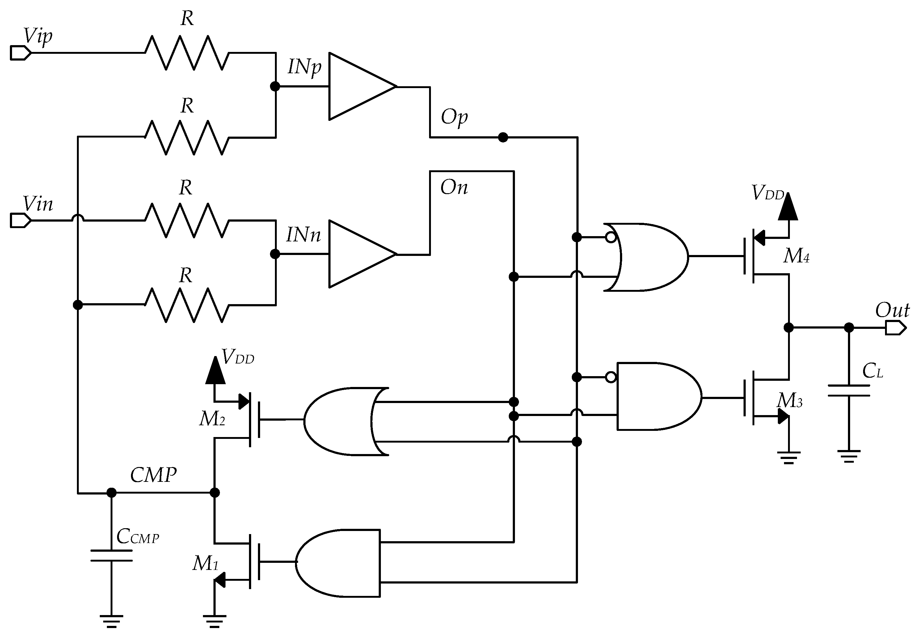
The implementation of the analog amplifier presented in [9] is reported in Figure 1. As explained in [9], the common mode (CM) extractor part in Figure 1 generates a common mode compensation analog signal to be added to the external inputs resulting in a common mode compensation method which is very similar to the common mode rejection mechanism of the conventional analog CMOS differential pair.
The CM compensation signal () is added to the external input signals by a summing network so that the actual input signals of the digital buffers can be expressed as:
and their differential mode (DM) and CM components are related to external DM () and CM () components as:
In Figure 1, a resistive summing network is included for the sake of simplicity, nonetheless, such a function can be conveniently implemented in CMOS technology by quasi-floating gate (QFG) techniques [9].
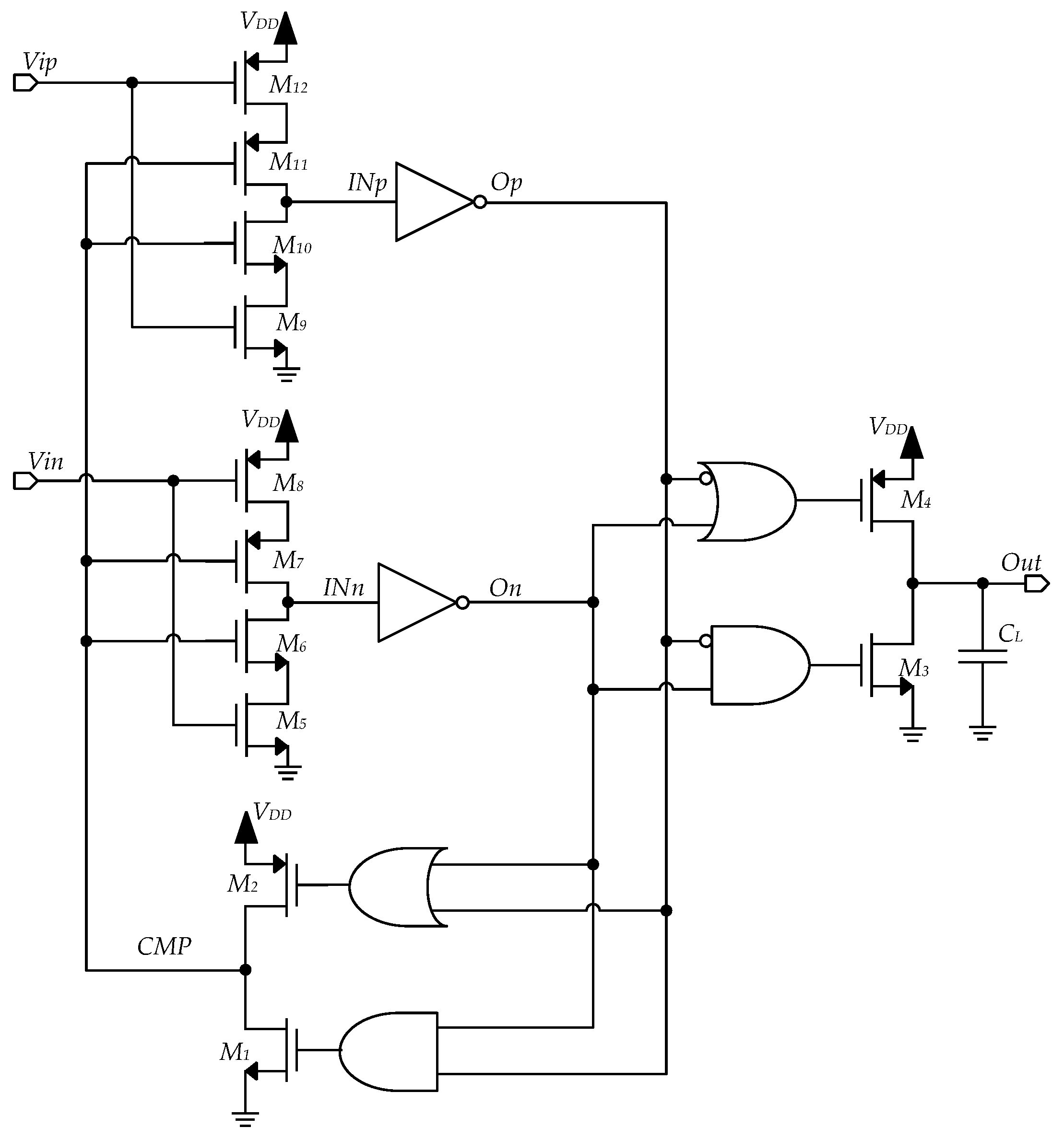
The evolution of the circuit in Figure 1, which avoids the passive components, but uses Muller C-elements reported in Figure 2. This idea was proposed in [10] and analyzed in detail in [12].
The Muller C-elements in Figure 2 implement, in a fully digital fashion, the compensation of the common-mode without requiring any calibration circuitry [10,11].
Even if QFG resistors and Muller C-elements can be implemented in CMOS processes, they are usually not available in the standard cell libraries provided by IC manufacturers, and all the previously reported digital OTA implementations are therefore not immediately suitable for automatic place and route within a semi-custom design flow.
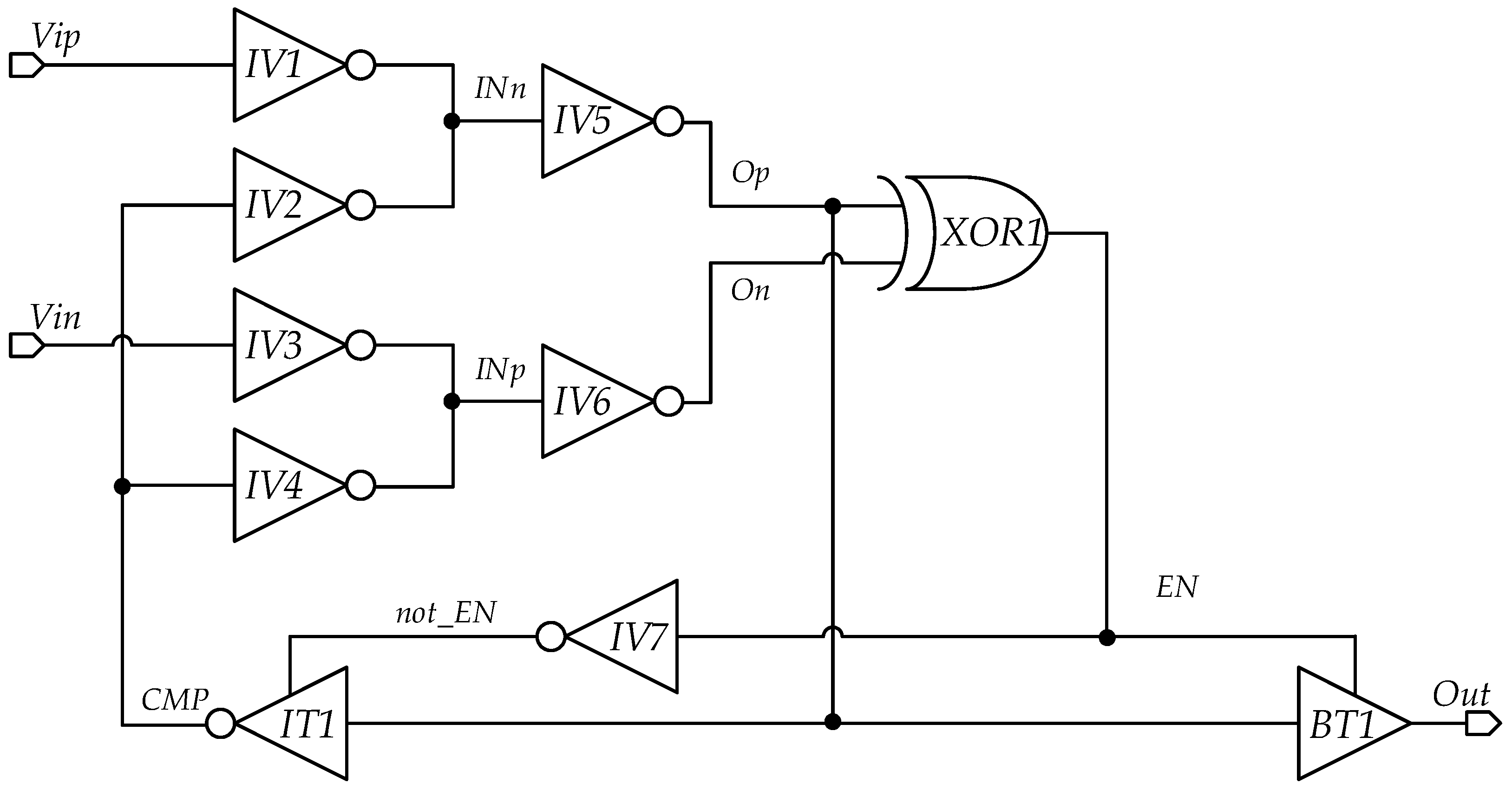
The schematic of the proposed pure standard cell implementation of the digital OTA is reported in Figure 3. In particular, the circuit in Figure 3 is based on the following types of logic gates:
- Inverter gates (IV);
- Exclusive OR gates (XOR);
- Three-state Buffer gates (BT);
- Three-state Inverter gates (IT).
Despite its pure standard cell implementation, the circuit operation is very similar to the one of the original implementations of the digital OTA in [9].
The CM extractor is implemented through the XOR1, the IV7 and the IT1 gates in Figure 3 and generates a common mode compensation signal () which is then added to the external inputs through the summing network implemented by inverter gates IV1, IV2, IV3 and IV4, thus compensating the common mode as happens in the conventional analog CMOS differential pair.
To explain the summing mechanism, it is sufficient to note that a CMOS inverter acts as a transconductor when its input voltage is close to the logic threshold, therefore, the output current of IV1 and IV2 (IV3 and IV4) are summed at their common output node and converted into a voltage through the equivalent resistance at node INn (INp).
3. Simulation Results
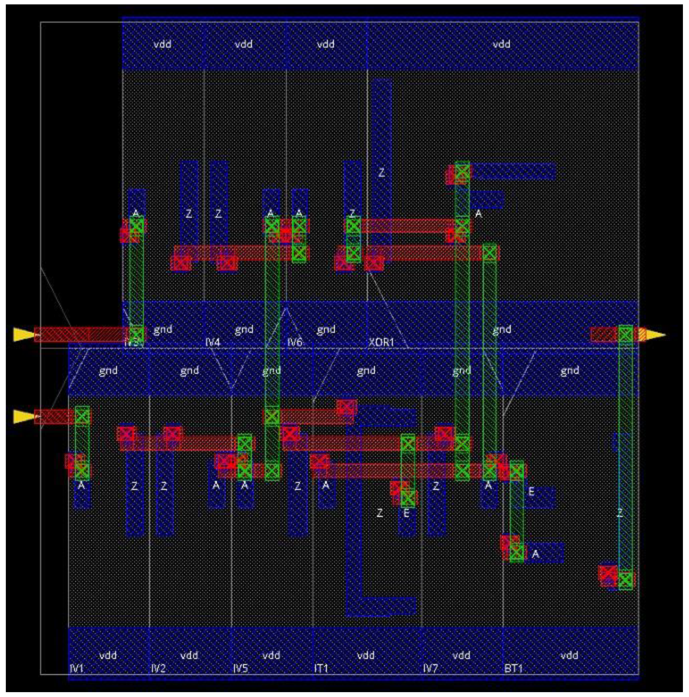
The proposed standard cell-based digital OTA (SC-DIGOTA) has been designed in the 130-nm STMicroelectronics CMOS technology adopting the standard cell library provided by the IC manufacturer. The circuit schematic has been described by using structural Verilog language (see Appendix A), and the layout has been automatically generated within the Cadence InnovusTM environment. Transistor level simulations on the post layout netlist have been carried out within the Cadence Virtuoso framework for analog design, exploiting AC and transient simulations. For AC simulations a bias point is established by applying the input signal on a DC level equal to about VDD/2 in order to have also the DC output voltage around VDD/2.
3.1. Automatic Place and Route
The automatically generated layout of the proposed digital OTA implementation is shown in Figure 4, showing an area footprint of 9.1 × 9.7.
3.2. Open Loop Simulations
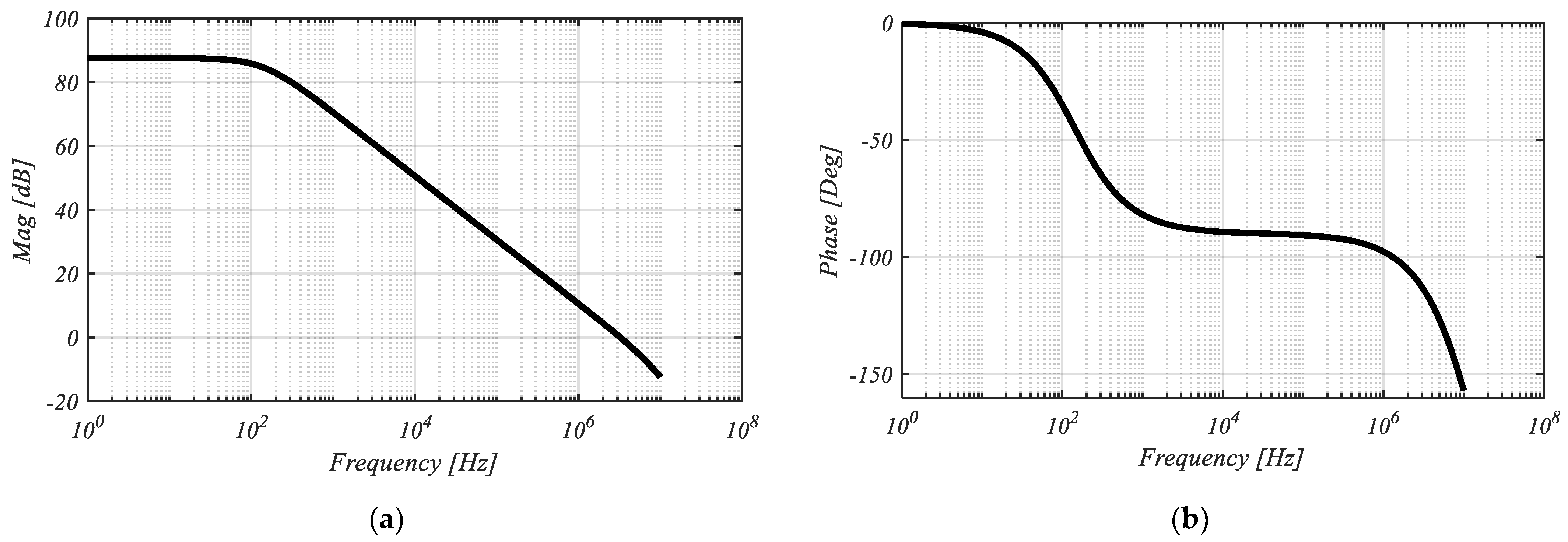
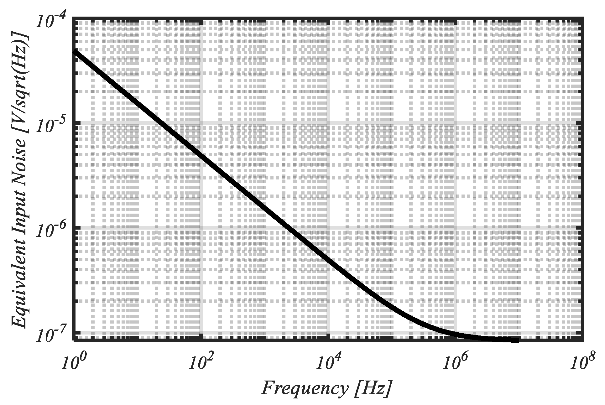
The amplifier has been simulated assuming a 0.55-V nominal supply voltage and a 250-pF load capacitance. The results of the open loop AC simulations of the proposed OTA are reported in Figure 5, showing that the digital OTA exhibits an overall DC gain and GBW of about 87 dB and 3.15 MHz, respectively. The phase margin of the amplifier results is higher than 65° with all the standard cells sized for minimum area. Figure 6 reports the input-referred noise plot of the proposed digital OTA showing an input-referred Flicker noise of about 4.82 @ 100 Hz and an input-referred white noise of about 175 @ 100 kHz.
3.3. Closed Loop Simulations
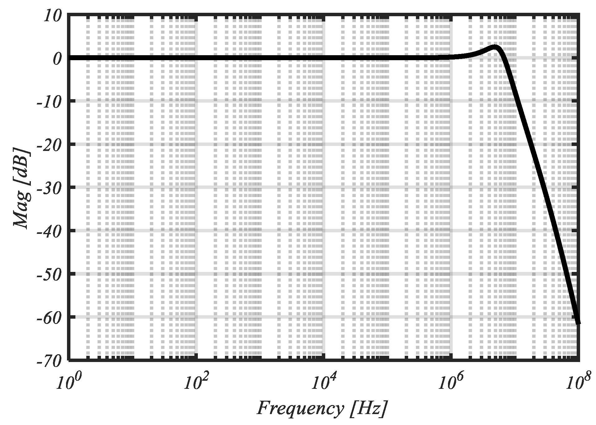
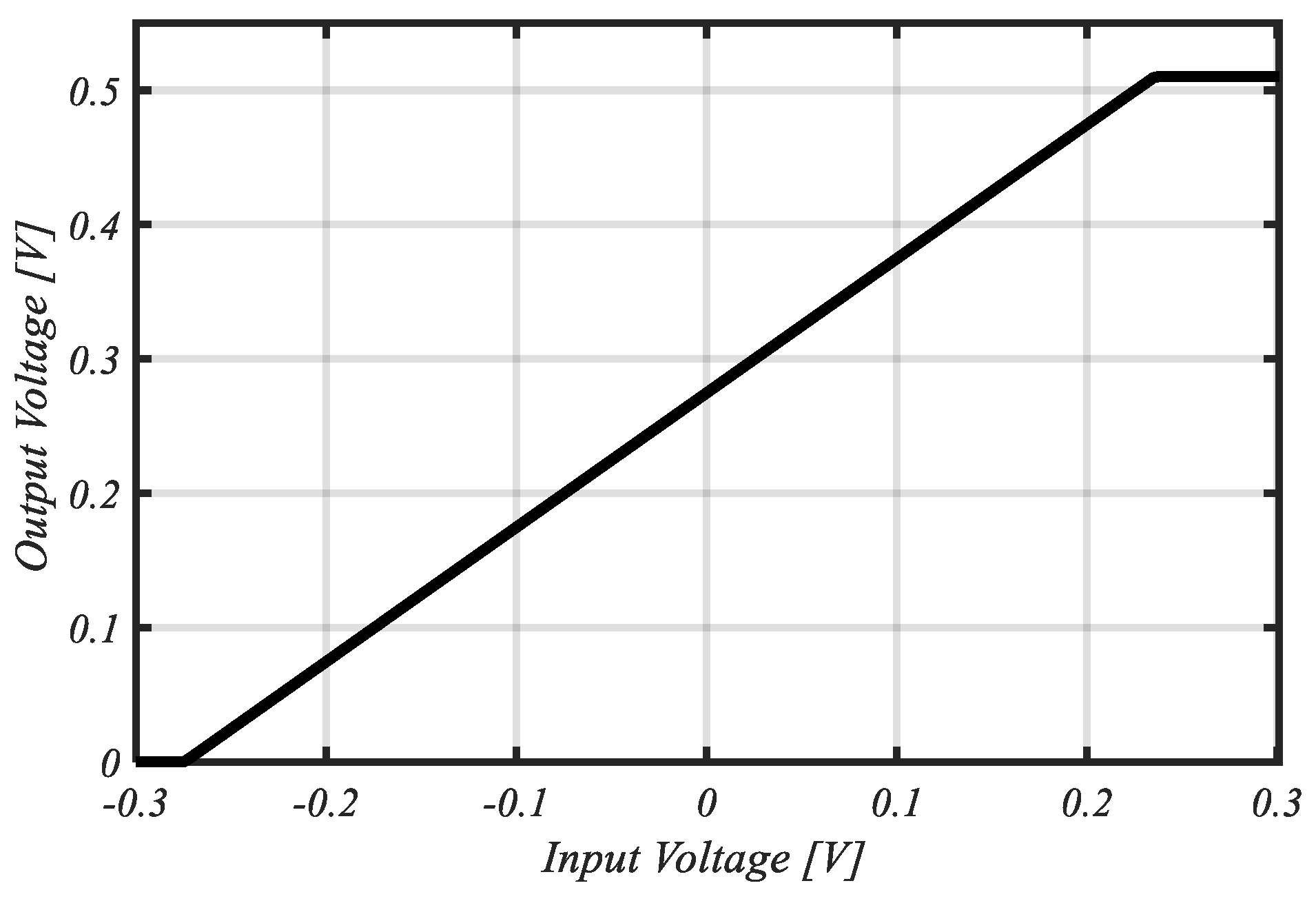
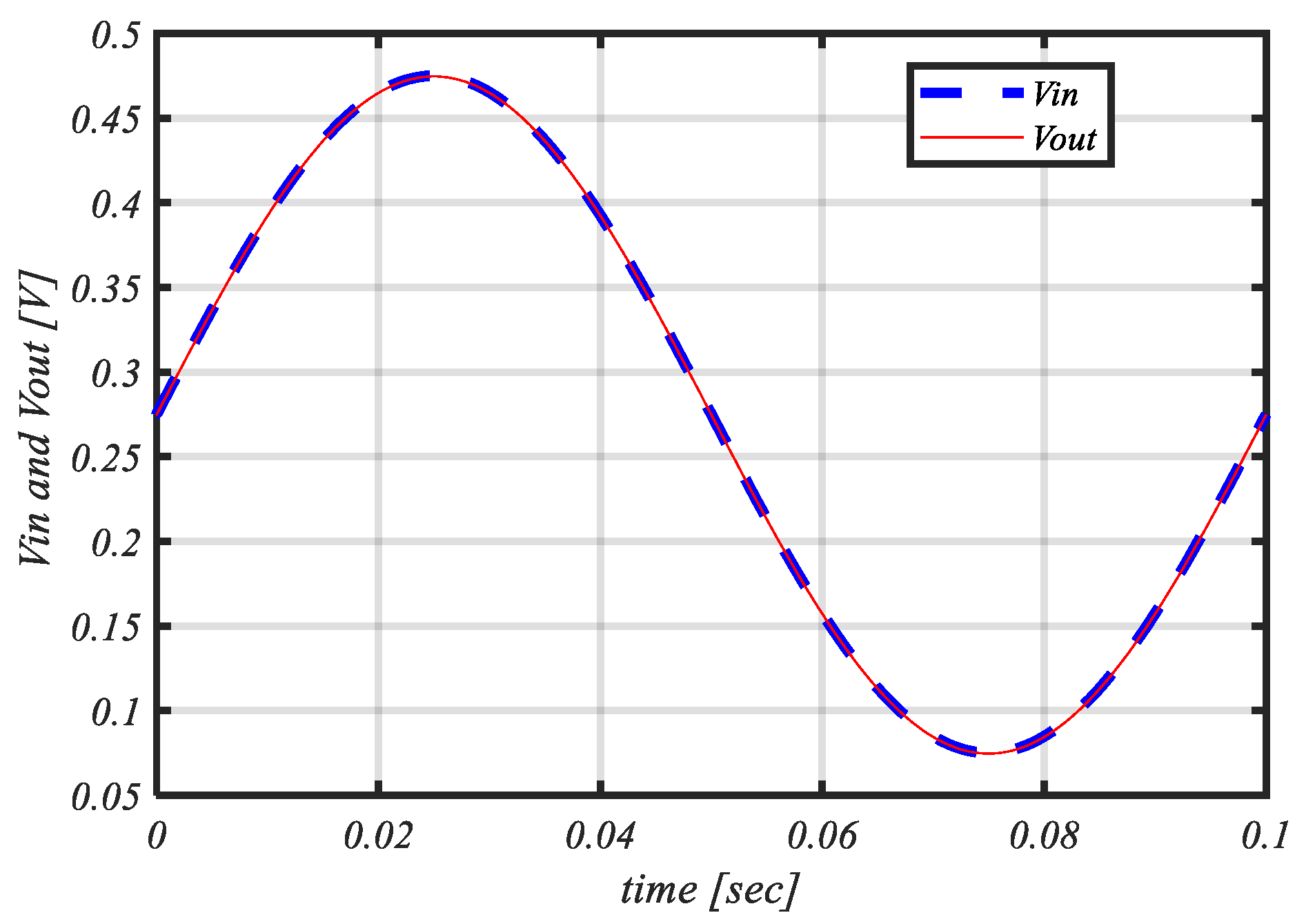
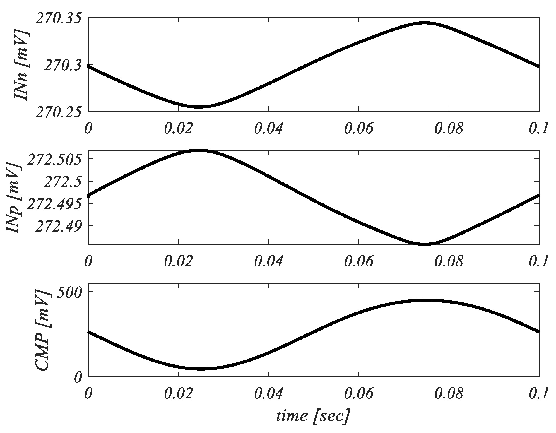
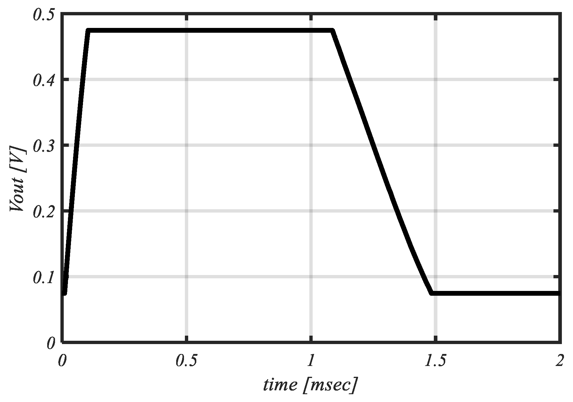
The OTA has then been simulated in a conventional non-inverting unity-gain configuration. The closed loop frequency response of the OTA is depicted in Figure 7, whereas the DC transfer characteristic is shown in Figure 8, highlighting an almost rail-to-rail behavior. Figure 9 shows the time domain response of the circuit to a sinusoidal waveform with a frequency of 10Hz and an amplitude of 200mV. The waveforms of the internal signals INn, INp and CMP of the SC-DIGOTA when processing the sinusoidal signal reported in Figure 9 are reported in Figure 10. Figure 11 shows the time domain response of the circuit to a square wave with a period of 2ms and an amplitude of 200mV. The positive and negative slew-rate have been found to be SR+ = 4.32 V/ms and SR− = 1.03 V/ms respectively.
4. Comparison with the Literature
To compare the proposed SC-DIGOTA against state-of-the-art low voltage amplifiers, we refer to the following Figures of Merit:
where is the gain bandwidth product, the load capacitance, is the average slew-rate, and is the power consumption. and in (3) and (4) denote small-signal and large-signal, respectively, while the and are normalized with respect to the layout area of the OTA.
Table 1 reports the comparison of the SC-DIGOTA against recently published low voltage OTAs taken from the literature, showing how the proposed circuit exhibits very good small signal performance and adequate large signal performance. Due to the very compact layout, the proposed OTA outperforms all other similar designs in terms of .
However, it has to be noted that, as pointed out in [16,17], the operation of Digital OTAs is typically strongly sensitive to PVT variations and mismatch, and often requires suitable calibration strategies to achieve high production yield. This also apply to the proposed implementation in which some sort of calibration [16,17] and/or VDD adjustment strategy is required to cope with variations.
5. Conclusions
In this paper, a digital OTA which, unless the others in literature, is realized with only digital gates of a standard cell library is proposed and demonstrated. The post layout circuit, resulting from a fully automatic design process, was simulated in open and closed loop conditions, which completely validate the idea.
In order to compare the performance of the proposed SC-DIGOTA with respect the previously DIGOTAs presented in literature, well-known figures of merits have been used. The comparison shows that added to main strength deriving by the fully standard cell realization, which gives significant advantages in the design step. The SG-DIGOTA results are also very competitive in the small signal domain, especially considering the very small silicon area required, while performing less in the large signal domain.
Author Contributions
Conceptualization, G.S.; methodology, G.S. and G.P.; software, G.S.; validation, G.S. and G.P.; writing—original draft preparation, G.S. and G.P.; writing—review and editing, G.S. and G.P. All authors have read and agreed to the published version of the manuscript.
Funding
This research received no external funding.
Data Availability Statement
The data presented in this study are available in article.
Conflicts of Interest
The authors declare no conflict of interest.
Appendix A
Verilog netlist of the SC-DIGOTA is as follows:
module SC-DIGOTA (input Vip, input Vin, output Out);
wire INn;
wire INp;
wire CM;
wire EN;
wire not_EN;
wire OP;
wire ON;
IVLL IV1(.A(Vip),.Z(INn));
IVLL IV2(.A(CM),.Z(INn));
IVLL IV3(.A(Vin),.Z(INp));
IVLL IV4(.A(CM),.Z(INp));
IVLL IV5(.A(INn),.Z(OP));
IVLL IV6(.A(INp),.Z(ON));
IVLL IV7(.A(EN),.Z(not_EN));
EOLL XOR1(.A(OP),.B(ON),.Z(EN));
BTSLL BT1(.A(OP),.E(EN),.Z(Out));
ITSLL IT1(.A(OP),.E(not_EN),.Z(CM));
endmodule
References
- Alioto, M. Enabling the Internet of Things: From Integrated Circuits to Integrated Systems; Springer: Berlin/Heidelberg, Germany, 2017. [Google Scholar]
- Liu, J.; Park, B.; Guzman, M.; Fahmy, A.; Kim, T.; Maghari, N. A Fully Synthesized 77-dB SFDR Reprogrammable SRMC Filter Using Digital Standard Cells. IEEE Trans. Very Large Scale Integr. (VLSI) Syst. 2018, 26, 1126–1138. [Google Scholar] [CrossRef]
- Aiello, O.; Crovetti, P.; Alioto, M. Standard Cell-Based Ultra-Compact DACs in 40-nm CMOS. IEEE Access 2019, 7, 126479–126488. [Google Scholar] [CrossRef]
- Fick, L.; Fick, D.; Alioto, M.; Blaauw, D.; Sylvester, D. A 346 μm 2 VCO-Based, Reference-Free, Self-Timed Sensor Interface for Cubic-Millimeter Sensor Nodes in 28 nm CMOS. IEEE J. Solid-State Circuits 2014, 49, 2462–2473. [Google Scholar] [CrossRef]
- Richmond, J.; John, M.; Alarcon, L.; Zhou, W.; Li, W.; Liu, T.T.; Alioto, M.; Sanders, S.R.; Rabaey, J.M. Active RFID: Perpetual wireless communications platform for sensors. In Proceedings of the 2012 ESSCIRC (ESSCIRC), Bordeaux, France, 17–21 September 2012; pp. 434–437. [Google Scholar]
- Paul, S.; Honkote, V.; Kim, R.G.; Majumder, T.; Aseron, P.A.; Grossnickle, V.; Sankman, R.; Mallik, D.; Wang, T.; Vangal, S.; et al. A Sub-cm3 Energy-Harvesting Stacked Wireless Sensor Node Featuring a Near-Threshold Voltage IA-32 Microcontroller in 14-nm Tri-Gate CMOS for Always-ON Always-Sensing Applications. IEEE J. Solid-State Circuits 2017, 52, 961–971. [Google Scholar] [CrossRef]
- Aiello, O.; Crovetti, P.; Alioto, M. Fully Synthesizable, Rail-to-Rail Dynamic Voltage Comparator for Operation down to 0.3 V. In Proceedings of the 2018 IEEE International Symposium on Circuits and Systems (ISCAS), Florence, Italy, 27–30 May 2018; pp. 1–5. [Google Scholar]
- Aiello, O.; Crovetti, P.; Lin, L.; Alioto, M. A pW-Power Hz-Range Oscillator Operating with a 0.3–1.8-V Unregulated Supply. IEEE J. Solid-State Circuits 2019, 54, 1487–1496. [Google Scholar] [CrossRef]
- Crovetti, P.S. A Digital-Based Analog Differential Circuit. IEEE Trans. Circuits Syst. I Regul. Pap. 2013, 60, 3107–3116. [Google Scholar] [CrossRef]
- Toledo, P.; Crovetti, P.; Aiello, O.; Alioto, M. Fully Digital Rail-to-Rail OTA with Sub-1000um2 Area, 250-mV Minimum Supply, and nW Power at 150-pF Load in 180 nm. IEEE Solid-State Circuits Lett. 2020, 3, 474–477. [Google Scholar] [CrossRef]
- Toledo, P.; Crovetti, P.; Klimach, H.; Bampi, S.; Aiello, O.; Alioto, M. A 300mV-Supply, Sub-nW-Power Digital-Based Operational Transconductance Amplifier. IEEE Trans. Circuits Syst. II Express Briefs 2021, 68, 3073–3077. [Google Scholar] [CrossRef]
- Toledo, P.; Crovetti, P.; Aiello, O.; Alioto, M. Design of Digital OTAs with Operation Down to 0.3 V and nW Power for Direct Harvesting. IEEE Trans. Circuits Syst. I Regul. Pap. 2021, 68, 3693–3706. [Google Scholar] [CrossRef]
- Chatterjee, S.; Tsividis, Y.; Kinget, P. 0.5-V analog circuit techniques and their application in OTA and filter design. IEEE J. Solid-State Circuits 2005, 40, 2373–2387. [Google Scholar] [CrossRef]
- Centurelli, F.; Della Sala, R.; Scotti, G.; Trifiletti, A. A 0.3 V, Rail-to-Rail, Ultralow-Power, Non-Tailed, Body-Driven, Sub-Threshold Amplifier. Appl. Sci. 2021, 11, 2528. [Google Scholar] [CrossRef]
- Centurelli, F.; Della Sala, R.; Monsurrò, P.; Scotti, G.; Trifiletti, A. A 0.3 V Rail-to-Rail Ultra-Low-Power OTA with Improved Bandwidth and Slew Rate. J. Low Power Electron. Appl. 2021, 11, 19. [Google Scholar] [CrossRef]
- Toledo, P.; Aiello, O.; Crovetti, P.S. A 300mV-Supply Standard-Cell-Based OTA with Digital PWM Offset Calibration. In Proceedings of the IEEE Nordic Circuits and Systems Conference (NORCAS): NORCHIP and International Symposium of System-on-Chip (SoC), Helsinki, Finland, 29–30 October 2019; pp. 1–5. [Google Scholar]
- Toledo, P.; Crovetti, P.; Klimach, H.; Bampi, S. Dynamic and static calibration of ultra-low-voltage, digital-based operational transconductance amplifiers. Electronics 2020, 9, 983. [Google Scholar] [CrossRef]
Figure 1.
Implementation of the digital-based analog amplifier presented in [9].
Figure 1.
Implementation of the digital-based analog amplifier presented in [9].

Figure 2.
Implementation of the DIGOTA presented in [10].
Figure 2.
Implementation of the DIGOTA presented in [10].

Figure 3.
Proposed fully standard cell Implementation of the digital OTA.

Figure 4.
Layout view of the SC-DIGOTA within the Cadence Innovus P&R tool.

Figure 5.
Frequency response of the SC-DIGOTA for CL = 250 pF, magnitude (a), phase (b).

Figure 6.
Equivalent input noise of the SC-DIGOTA.

Figure 7.
Closed loop frequency response.

Figure 8.
Closed loop dc voltage transfer characteristic.

Figure 9.
Time domain response to a sinusoidal waveform (frequency = 10 Hz and amplitude = 200 mV) of the SC-DIGOTA in unity gain configuration.
Figure 9.
Time domain response to a sinusoidal waveform (frequency = 10 Hz and amplitude = 200 mV) of the SC-DIGOTA in unity gain configuration.

Figure 10.
Internal waveforms of the SC-DIGOTA in unity gain configuration in response to a sinusoidal waveform (frequency = 10 Hz and amplitude = 200 mV).
Figure 10.
Internal waveforms of the SC-DIGOTA in unity gain configuration in response to a sinusoidal waveform (frequency = 10 Hz and amplitude = 200 mV).

Figure 11.
Time domain response to a square wave (period = 2 ms and amplitude = 200 mV) of the SC-DIGOTA in unity gain configuration.
Figure 11.
Time domain response to a square wave (period = 2 ms and amplitude = 200 mV) of the SC-DIGOTA in unity gain configuration.


Table 1.
Comparison against the state of the art.
| [13] | [14] | [15] | [12] | [12] | This Work | |
|---|---|---|---|---|---|---|
| supply voltage [V] | 0.5 | 0.3 | 0.3 | 0.3 | 0.5 | 0.55 |
| OTA architecture | bulk-driven | bulk-driven | bulk-driven | digital | digital | digital |
| technology [nm] | 180 | 130 | 130 | 180 | 180 | 130 |
| area (μm2) | 26,000 | 6400 | 3600 | 982 | 982 | 88.3 |
| cap load CL [pF] | 20 | 50 | 40 | 150 | 150 | 250 |
| power [μW] | 110 | 0.0114 | 0.073 | 0.0024 | 0.1075 | 8.2 |
| DC gain [dB] | 52 | 64.6 | 41 | 30 | 73 | 87 |
| GBW [kHz] | 2500 | 3.58 | 18.65 | 0.250 | 57.5 | 3150 |
| average slew rate SR [V/μs] | 2.89 | 0.00093 | 0.0216 | 0.000085 | 0.019 | 0.0027 |
| in-band input noise [μV] | 442.7 | - | - | 21 | 122 | 253 |
| CMRR [dB] | 78 | 61 | 67.4 | 41 | 65 | 46 |
| PSRR [dB] | 76 | 28 | 45 | 30 | 50 | 39 |
| FOMS [MHz∙pF/μW] | 0.45 | 15.7 | 10.2 | 15.6 | 80.2 | 96.6 |
| FOML [(V/μs)·pF/μW] | 0.52 | 4.07 | 11.8 | 5.3 | 26.5 | 0.58 |
| FOMS,A [MHz∙pFμW·mm2] | 17.3 | 2453 | 2833 | 15,885 | 81,724 | 1,094,000 |
| FOML,A [V/μs·pFμW·mm2] | 20.2 | 635.9 | 3277 | 5397 | 27,000 | 6568 |
Publisher’s Note: MDPI stays neutral with regard to jurisdictional claims in published maps and institutional affiliations. |
© 2021 by the authors. Licensee MDPI, Basel, Switzerland. This article is an open access article distributed under the terms and conditions of the Creative Commons Attribution (CC BY) license (https://creativecommons.org/licenses/by/4.0/).
Share and Cite
MDPI and ACS Style
Palumbo, G.; Scotti, G. A Novel Standard-Cell-Based Implementation of the Digital OTA Suitable for Automatic Place and Route. J. Low Power Electron. Appl. 2021, 11, 42. https://doi.org/10.3390/jlpea11040042
AMA Style
Palumbo G, Scotti G. A Novel Standard-Cell-Based Implementation of the Digital OTA Suitable for Automatic Place and Route. Journal of Low Power Electronics and Applications. 2021; 11(4):42. https://doi.org/10.3390/jlpea11040042
Chicago/Turabian StylePalumbo, Gaetano, and Giuseppe Scotti. 2021. "A Novel Standard-Cell-Based Implementation of the Digital OTA Suitable for Automatic Place and Route" Journal of Low Power Electronics and Applications 11, no. 4: 42. https://doi.org/10.3390/jlpea11040042
Note that from the first issue of 2016, this journal uses article numbers instead of page numbers. See further details here.