1. Introduction and Motivation
As edge computing on resource-constrained edge devices is gaining momentum, the need for a low-cost cryptosystem for these devices is also increasing. For public-key cryptography, elliptic curve cryptography (ECC) is regarded as a better solution in terms of security per bit, computation, and memory/storage requirements as compared to other public-key cryptographic approaches, such as RSA [
1]. This is mainly due to ECC’s shorter key length as compared to RSA under comparable security levels. The ECC’s shorter key length also leads to a reduction in computing complexity and storage cost. These characteristics make ECC more attractive to resource-constrained systems (e.g., edge devices), which require acceptably high security levels with performance and resource constraints [
2].
Although cracking ECC has proven to be a mathematically difficult problem, the advent of cryptanalytic attacks on implementations, also known as side-channel attacks (SCAs), has overturned this traditional concept through a fine-grained analysis of sensitive leakages, such as timing, power, visible light, electromagnetic emanations, and acoustic side-channel information [
3]. Various hardware-based countermeasures to resist SCAs have been proposed in [
4,
5]. In [
4], Liao et al. applied binary randomized montgomery operation (RMO) to modular arithmetic to design an ECC coprocessor that is resistant to non-invasive SCAs. In [
5], Lee et al. proposed a power-analysis-resistant dual-field ECC processor using heterogeneous dual-processing-element architecture. The authors implemented priority-oriented scheduling of right-to-left double-and-add-always elliptic curve scalar multiplication with a randomized processing technique to achieve a power-analysis-resistant dual-field ECC processor.
Many of the existing ECC processors are based on sequential circuits (or synchronous circuits) (e.g., [
4,
5]). This is mainly because of the ease of design and verification of synchronous sequential circuits as compared to asynchronous circuits. However, from a security perspective, the synchronous sequential circuits consume more power and energy (due to the increased clock rates and clock generation/distribution circuits), which in turn make these circuits more susceptible to power-/energy-analysis attacks. Furthermore, an attacker can easily isolate the operation time of a certain logic-switching activity by referring to the clock signals, making the side-channel analysis much easier than the asynchronous circuits. Additionally, almost all of the state-of-the-art SCAs are targeted for sequential circuits. These attack methodologies are, however, not always appropriate to attack combinational circuits. For example, hamming weight- and hamming distance-based power models used in differential power analysis (DPA) and correlated power analysis (CPA) attacks are only suitable for power characterization of registers and buses (note that here we focus only on hardware security attacks and not on the software/algorithmic vulnerabilities of ECC). Yet, neither of these models are suitable for large-scale, multi-input combinational circuits [
6,
7]. Hence, we propose to design an ECC processor as a pure asynchronous combinational circuit.
SCAs against combinational circuits have not been extensively explored but, from recent research works, we know that they are not immune to such attacks [
8,
9]. Zheng [
6] proposed an SCA called a power template match attack that is effective against combinational circuits. This attack is able to crack the S-box (implemented as a combinational circuit) of PRINTcipher. To mount this attack, first, the authors built a power model template based on the input transitions of the combinational circuit (i.e., S-box). Using this power model template, they estimated the average power consumption of the modeled combinational circuit. Then, they implemented the combinational circuit in hardware and measured the actual power consumption. By correlating the average power consumption values obtained from the power model template with the average values of actual power consumption, they were able to recover the secret key. This attack works on combinational circuits designed using the standard-cell libraries based on forward application-specific integrated circuit (ASIC) design flow with a synchronous design style. Therefore, it is apparent that security risks exist in the standard-cell-based design flow because it has no special consideration for protection of combinational circuit design.
To prevent SCAs against combinational circuits, it is necessary to migrate the design approach to non-conventional combinational logic. We leverage this principle in the design of our secure and robust ECC processor, wherein we employ a genetic algorithm (GA) to evolve a non-conventional combinational circuit. GA is a pseudo-random algorithm that can generate multiple, functionally equivalent circuits. We can randomly select a circuit from the pool of functionally equivalent circuits generated by our GA as our ECC processor. This makes power template match attacks (e.g., those illustrated in [
6]) inaccurate against our ECC processor because power template match attacks require an attacker to design the same circuit to generate the power model template. Moreover, Zheng [
6] was successful at mounting an attack on an S-box of PRINTcipher which has 5-bit input and 3-bit output. The small input length (5-bit) made the design of a power model template feasible because the circuit has only
possible input transitions. However, our elliptic curve cryptosystem will have a 160-bit input, which will have
possible input transitions. It is apparent that it will be infeasible to take into account all of these input transitions to build an effective power model template to mount the power template match attack proposed in [
6]. Although GAs have been used for constructing the security components of cryptosystems, such as AES S-Boxes in [
10,
11], prior works have not applied GA for designing combinational circuits for ECC. Furthermore, our GA employs a multi-objective fitness function, which has not been used in prior works [
10,
11].
Apart from power-analysis, there are several other attack surfaces that can be employed for SCA in combinational circuits. An SCA on combinational circuits may be performed using information leaked through glitches, early propagation, unstable power traces, and dependencies of circuit delays on input data. Glitches in a combinational circuit (caused by toggling of gates before final values are settled) can potentially leak information through the side-channels [
12]. In addition, the early propagation phenomenon, in which logic gates evaluate their outputs before all inputs have settled, can also leak important information via side-channels [
13]. As a countermeasure for these attack surfaces, we transform the non-conventional combinational circuit design of our ECC processor to a multi-threshold dual-spacer dual-rail delay-insensitive logic (
) paradigm [
14] (see
Section 5). This work is an extension of our earlier work [
15], in which we used a GA to address the vulnerability of ECC to SCAs by evolving combinational logic circuits that correctly implemented ECC hardware that was resistant to timing and power analysis attacks. However, our earlier work [
15] did not utilize
for GA-based evolving combinational circuits. Furthermore, our earlier work [
15] did not propose a secure and dependable ECC processor that utilized the proposed GA-based evolving combinational circuits.
In this work, we transform the GA-based evolving combinational circuits to the
paradigm to provide stronger resilience against SCAs, as compared to prior works.
removes the dependency on clock signals and implements a delay-insensitive hand-shake protocol to perform operations asynchronously within the circuit. This allows designers to mask the start times and end times of operations of different sub-blocks of the circuit or instruction-processing, thus providing flatter power traces and more constant energy consumption. Additionally,
circuits possess benefits of delay-insensitive asynchronous circuits, such as having no clock tree, high energy efficiency, robust circuit operation under process/voltage/temperature variations, and low noise/electromagnetic emission. These characteristics enhance the robustness of the
circuits against SCAs [
13,
14,
16].
In summary, we make the following contributions.
We propose the design of a side-channel attack-resistant asynchronous circuit for scalar multiplication in an elliptic curve over the prime field. We leverage the genetic algorithm with a multi-objective fitness function to generate a standard Boolean logic-based combinational circuit for scalar multiplication. We transform this circuit into a circuit by replacing the standard Boolean logic gates of the combinational circuit with gates and adding a register interface and early completion detection logic. We then design point-addition and point-doubling circuits using the same procedure.
We integrate scalar multiplication, point-addition, and point-doubling circuits to design a secure, dependable, and robust ECC processor using a system-on-chip field-programmable gate array (SoC FPGA). Dependability is provided by using our novel fault tolerance using self-reconfiguration in dual modular redundant system (FT-SR-DMR) scheme.
We perform functional verification of the proposed circuit using Xilinx ISE and implement it on a Xilinx Kintex-7 FPGA.
We analyze the resilience of our proposed circuit against timing analysis, power analysis, and fault analysis attacks.
The remainder of this article is organized as follows.
Section 2 describes the security threat model assumed for this work.
Section 3 presents the SCA vulnerabilities of ECC and existing countermeasures.
Section 4 illustrates the generation of combinational circuits for scalar multiplication in ECC using a genetic algorithm.
Section 5 elaborates the conversion of combinational circuit for scalar multiplication generated by our proposed genetic algorithm into an
-based design that is resilient to both power- and timing-based SCAs. The high-level architecture of our proposed secure and dependable ECC processor is described in
Section 6.
Section 7 analyzes the security of the proposed elliptic curve cryptosystem against various types of attacks mentioned in our threat model. Experimental results and analyses are presented in
Section 8. Finally,
Section 9 concludes this work.
3. SCA Vulnerability of ECC Scalar Multiplication and Existing Countermeasures
SCAs have proven to be extremely effective as a practical means for attacking implementations of cryptographic algorithms, especially in constrained devices, such as chip-cards, where straightforward implementations of cryptographic algorithms can be broken with minimal units. In this section, we provide a digest of existing attacks and countermeasures.
Timing and simple power analysis SCAs: Timing attacks can be mounted by exploiting the timing variance for different input values [
18]. Timing variations can be caused by cache (e.g., time for instruction execution in case of cache hit and miss are different) or conditional branches. Simple power analysis attacks on cryptographic implementations can be performed if the power traces show distinctive key-dependent patterns [
18]. For example, difference in power consumption of point-doubling and point addition in double-and-add algorithms can reveal the value of secret keys.
Differential side-channel analysis attacks: Differential side-channel analysis attacks (DPA, short for differential power analysis, and DEMA, short for differential electromagnetic analysis) pry out secret information from measurements of power or electromagnetic emanations by using statistical techniques [
19]. Differential SCAs require leakage from side-channels to be larger than noise. Leakage is distinguished from noise by averaging samples of leaked data generated from a large number of same key operations.
Refined power analysis and zero-value analysis attack: Refined power analysis (RPA) attacks infer secret information by using search algorithms to find special points
on the elliptic curve, having one coordinate as zero (e.g.,
). The attacker assumes some specific bits of the secret key and uses an algorithm to search for
, by feeding guess points
P to the system. When the search algorithm succeeds in finding the special points, the intermediate results of the algorithm can be analyzed to speculate the correctness of the assumed bits of the secret key [
20]. Zero-value point attacks (ZPAs) are a special case of RPA. ZPAs work even if the search algorithm fails to find special points
on the elliptic curve. In ZPAs, the attacker can extract secret information from cases when the values in the auxiliary registers of elliptic curve point addition and point-doubling operations in Jacobian coordinates become zero [
21].
Template attack: Template attacks determine secret information through precise multivariate characterization of signals and noise of a target system by using detailed profiles of signals and noise of identical experimental systems [
22]. Template attacks are the strongest form of SCAs possible in an information theoretic sense because they utilize all possible information (both signal and noise) available in each sample of leaked information. Template attacks are thus in sharp contrast with other statistical methods (e.g., DPA, CPA, RPA, etc.) which consider noise as a hindrance and focus on eliminating noise by averaging over a large number of samples of leakage data.
Fault attacks: Fault attacks are carried out by actively disturbing the cryptographic devices by inducing faults and exploiting the abnormal behavior of the victim device to derive secret information [
23]. Faults can be injected using different methods, such as changing a bit in memory with laser, violating the setup time with glitches in the clock, or abnormally lowering the supply voltage. The precision of the time and location of fault injections has a significant impact on the success rate of fault attacks. Fault attacks can be classified into three categories: safe-error-based analysis, weak-curve-based analysis, and differential fault analysis. Differential fault analysis attacks analyze the difference between correct and erroneous outputs to retrieve the secret bit-by-bit [
24].
There are multiple possible methods proposed to thwart most of the attacks discussed above. The attacks and their existing countermeasures are listed in
Table 1. In this article, we propose a new cryptographic circuit design paradigm based on a genetic algorithm and
logic to thwart simple and differential side-channel analysis attacks.
4. Generation of Combinational Circuit for Scalar Multiplication Using Genetic Algorithm
GAs are widely used algorithms, which can be applied to various applications. For security and cryptography, GAs have been used to construct components for cryptographic algorithms (e.g., S-boxes in AES [
10,
11]). Other than these applications, the GAs can also be used as an engine to discover new designs of digital circuits because they allow one to explore a much larger space of possible designs [
33,
34,
35,
36]. In addition to digital circuit designs, designs generated by GA are often different from those created by top-down, human, rule-based design approaches (such as designing digital circuits using standard cell libraries based on forward ASIC design flow).
Figure 1a shows the design of a full adder circuit using the Boolean algebra, truth table, and K-map. The same full adder circuit is generated by using GA with
circuit configurations which has nine gates, connected as shown in
Figure 1b. In order to compute the propagation delay of the critical path of our evolved circuit, we represent the evolved combinational circuit as a directed acyclic graph, as shown in
Figure 1c. The potential advantage of using non-conventional combinational circuits designed using GA is that it can improve the resistance of the circuit against certain SCAs for which an attacker needs to build an exact prototype of the circuit. In addition, usually the evolved circuits are found to be more efficient (in terms of size and propagation delay) than those created using traditional design methods [
35]. In this work, we use a GA to generate combinational circuits that perform scalar multiplication in an elliptic curve over the prime field. We chose scalar multiplication because it is the most critical operation in ECC and there are numerous SCAs performed on scalar multiplication [
34]. In this work, we fix the size of a secret key to 6-bit, and base point to 5-bit. Our future plan is to design a full-sized combinational circuit that supports 160-bit key length.
In this section, we first delineate the fundamentals of ECC. Then, we describe the representation of a combinational circuit for scalar multiplication as a chromosome in our GA. Next, we elaborate on the multi-objective fitness function used in our GA. Finally, we explain the core genetic algorithm used to generate the combinational circuit for scalar multiplication.
Elliptic Curve Cryptosystem and Scalar Multiplication: ECC [
37] is based on the algebraic structure of elliptic curves over finite fields. For our work, we use an elliptic curve over prime field
, where the prime number
. Equation (
1) shows the elliptic curve we employ for our ECC. The coefficients
and
are set to 4 and 20, respectively.
Figure 2 shows the points in the elliptic curve of Equation (
1).
In the public key generation step of ECC, the scalar multiplication involving the base point on the elliptic curve is the critical operation. The base point is a point chosen from the points in
Figure 2. The scalar value used in the scalar multiplication operation is the secret key or private key. In this work, we used a secret key with 6-bit length. The security of elliptic curve-based security applications and protocols relies on an elliptic curve discrete logarithm problem—the inability to compute the secret scalar value given the base point and public key.
Scalar multiplication between a point
and a scalar
k is denoted by
and is computed using a Double-and-Add algorithm (Algorithm 1) [
18]. We implement the Double-and-Add algorithm for computing the functional correctness (one of the objectives in a multi-objective fitness function of our GA) of the evolved circuit.
| Algorithm 1 Double-and-Add algorithm for scalar multiplication in ECC [15]. |
| Input: Elliptic curve , an elliptic curve point N, and scalar k of bits. |
| Output:M = kN |
| t = number of bits of k |
| = prime number |
| Initialization: |
| |
| Core Algorithm: |
| for downto 0 do |
| |
| if then |
| |
| end if |
| return (M) |
| end for |
Encoding a Combinational Circuit as a Binary Chromosome: In GA, a solution is represented by a chromosome and a fitness value associated with the chromosome. A chromosome is usually represented as a string of binary values, 0’s and 1’s. In our digital circuit design problem, the solution is a combinational circuit. Thus, we use a 2D binary chromosome for encoding the combinational circuit into a genotype (
Figure 3). The 2D binary chromosome has a size N×M, where N is the number of vertical levels (numbered from 0 to N − 1) and M is the number of logic gates in each level. We use eight different types of Boolean logic gates which are shown in
Table 2. In that account, three bits are used to represent a gate in binary. Thus, the GATE_ID in
Figure 3 is three bits wide. The logic gates in Level 0 have two functions. First, these gates act as input interface which take input signals from external sources. Second, these gates group with gates in Level 1 to level N-1 to form a functional combinational circuit that performs scalar multiplication. The outputs from gates at level N produce the overall circuit output values which is the product of the scalar value and base point.
As shown in
Figure 3, each gate has two inputs and one output. The outputs of the gates at each level are indexed by numbers from 0 to M. These outputs are connected to inputs of the gates at the next level. Hence, the inputs of the gates at a level are also indexed by a number from 0 to M. Therefore,
bits are needed to encode an index (IP1_ID and IP2_ID in
Figure 3) in binary. The inputs to a gate at level
i can be the output from any gate at level
. Finally, the length of chromosome is given by M * (GATE_ID + (N − 1) * (IP1_ID + IP2_ID + GATE_ID)).
We used GA to design four different combinational circuits. These circuits differ in the number of base points they support. A
circuit can support points enclosed in rectangle A in
Figure 2 as a base point for scalar multiplication. In other words, a
circuit can perform correct multiplication of any six-bit secret key with any point in rectangle A in
Figure 2. Similarly,
,
, and
circuits can perform correct scalar multiplication of any six-bit secret key with any point enclosed in rectangle B, C, and D in
Figure 2, respectively.
Multi-objective Fitness Function: A primary operation involved in GA is the evaluation of adherence of evolved solutions to the imposed constraints. GA uses a fitness function to evaluate the competence of evolved solutions. We use a multi-objective fitness function for our GA which is based on aggregation by variable objective weighting [
38]. In aggregations by the variable objective weighting scheme, the fitness function is represented as the weighted sum of the objectives. Each objective is assigned a weight
such that
, and the scalar fitness value is calculated by summing up the weighted objective values
. In our case, there are three governing constraints (or objectives), viz., correctness in input/output behavior, minimization of propagation delay, and minimization of the size of the evolved circuit.
for correctness in input/output behavior is set to
and
for circuit size and propagation delay are set to
and
, respectively.
In order to quantify the correctness in input/output behavior, we incorporate the notion of expected output and observed output. A reward function
is defined, which counts the number of observed outputs that are equal to the expected outputs. The count is considered as reward value.
, where
represents the simulation inputs (refer
Figure 2) which are the points on the elliptic curve. We used these simulation points to check the correctness in input/output behavior of the evolved combinational circuit.
represents the expected output of the circuit with
as an input and
represents the observed output of the evolved combinational circuit. The expected output is computed by implementing the double-and-add scalar multiplication algorithm.
Our other design objective is the minimization of the size of the evolved circuit. We estimate the necessary area for an evolved circuit using the concept of gate equivalence [
39], which is a basic unit of measure for digital circuit complexity. This measure is more accurate than the simple number of the gates concept. We formulate a function,
, to represent the gate-equivalent value of an evolved circuit. Our final objective is minimization of the propagation delay of evolved circuit. The finite time that a circuit takes to reflect the change in input on its output values is known as propagation delay. Propagation delay is different for different gates. We measured the propagation delay using the path having the highest delay, called the worst-case delay path (or critical path). The
represents the delay function in our fitness function. We employ the representation of a combinational circuit as a directed acyclic graph to compute the critical path (as shown in
Figure 1). The gate-equivalent values and propagation delay values for the gates in our evolved circuit are shown in
Table 2. The following equation shows the fitness function we used for our GA.
Genetic Algorithm: For the genetic algorithm, we have employed a CHC-adaptive search algorithm [
40] with the parameter settings listed in
Table 3. The CHC algorithm is based on the elitist selection method that uses a high probability of crossover (
) and no mutation. In the following, we elaborate the working of our version of CHC GA. For initialization, we randomly select a group of individuals (combinational circuits), which are then set as the starting point of the algorithm. These individuals are represented by a data structure having a chromosome and a fitness value of chromosomes as components. These initial sets of individuals constitute a parent population, which we denote as
.
The GA solution advances by spawning a child population () from the parent population by using a reproduction operator called crossover operator. During the crossover, the GA selects two random individuals (i.e., parents) from . Before performing the crossover operations, one needs to check whether the hamming distance (HD) of the parents is greater than or equal to a certain threshold (denoted as ) or not. If the requirement is satisfied by the two individuals (parents), the crossover operation can be carried out. This mechanism is known as incest prevention in CHC GA. For crossover operation, a half of the bits from the random chromosome locations that are different in the two parents are exchanged. This type of crossover is referred to as half-uniform crossover. In case the requirement for is not satisfied, is decremented by one, and another parent (i.e., two individuals) is selected randomly for crossover. This process continues until the GA finds parents eligible for crossover/mating. However, in case of convergence in local maxima, will keep decreasing and hit zero value without finding any eligible parents for mating. At this point, the CHC GA is restarted with the initial population of elite individuals (i.e., individuals with the best fitness value) from the current parent population. The remaining population () (i.e., individuals) are generated by randomly flipping bits of the elite individuals.
The crossover operations in the CHC GA generate the child population. To produce the next generation of individuals, both the the child and parent population are merged into a single pool, and the individuals are sorted in the descending order of the fitness value. A total of individuals having the best fitness values are selected as parents for producing the next generation of child populations.
5. Converting Combinational Circuit into Asynchronous Circuit
The focus of digital design has primarily been on synchronous, clocked architectures over the last three decades. However, as clock rates have significantly increased while feature size has decreased, clock skew has become a major problem. To achieve acceptable skew, high-performance chips must dedicate increasingly larger portions of their area for clock drivers. This causes these chips to dissipate increasingly higher power. As these trends continue, the clock is becoming more and more difficult to manage, while clocked circuits’ inherent power inefficiencies are emerging as the dominant factor hindering increased performance. Furthermore, increased power consumption makes these circuits susceptible to power analysis SCAs. These issues have caused renewed interest in asynchronous digital design. Asynchronous, clockless circuits require less power, generate less noise, and produce less electromagnetic interference (EMI), compared to their synchronous counterparts. Furthermore, delay-insensitive asynchronous paradigms provide additional advantages, including substantially reduced crosstalk between analog and digital circuits, ease of integrating multi-rate circuits, and facilitation of component reuse. Currently, companies such as ARM, Phillips, Intel, and others are incorporating asynchronous logic into some of their products using their own proprietary tools.
In this section, we convert the non-conventional combinational circuit for scalar multiplication generated by our GA into a
-based design that is capable of mitigating both power- and timing-based SCAs [
34].
5.1. Multi-Threshold Dual-Spacer Dual-Rail Delay-Insensitive Logic
()
[
14] is a delay-insensitive asynchronous logic family. It is developed by combining the dual-spacer dual-rail delay-insensitive logic (
) [
13] with the multi-threshold NULL convention logic (MTNCL) [
16] paradigm. The logic gates and registers of
are the same as those of
. However, the input-incompleteness [
41] of
is rectified by incorporating the sleep signal concept of MTNCL.
represents a signal with three states: DATA0, DATA1, and NULL (or spacer) state as shown in
Table 4. These states are coded using two rails (or wires). Asserting a TRUE value on Rail0 represents DATA0 and asserting a TRUE value on Rail1 represents DATA1. There are two NULL (or spacer) states in
representation: all-zero-spacer, and all-one-spacer. The
dual-spacer protocol sequence is shown in
Figure 4g. As shown in the protocol, a
circuit must return to the spacer after one data cycle before starting a new data cycle. In other words, the data and spacer must alternate in a
circuit. This ensures that the number of times each dual-rail signal switches is independent from the input data. The only information that the switching reveals is the number of data values processed which makes power variation significantly smaller than synchronous designs. In addition, in
circuit, altering from an all-zero-spacer to all-one-spacer after every data set (as shown in
Figure 4g) allows both rails to have identical switching activity regardless of the data being processed. Therefore, the difference in switching activities between these two rails does not cause much difference in power consumption. Hence, it is hard for an attacker to decode which rail is switching based on the power consumption variation between two rails.
5.2. Gates, Registers, and Early Completion-Checking
Gates: The basic gates used in
logic family are the gates of
logic family. Here, we briefly describe the basic gates of
logic family.
logic family consists of 27 basic gates called threshold gates [
42]. These 27 gates constitute the set of all functions consisting of four or fewer variables. Each
gate has
n inputs and a threshold value
m, and the gate is denoted as
. For example, a
gate has A, B, and C as its inputs, and will only assert its output when two or more of its inputs have been asserted. All basic gates of standard Boolean logic can be converted into threshold gates.
Figure 4a–f shows the threshold gate version of the basic Boolean logic gates.
Registers: In , each combinational block should be bracketed by input and output register stages to alternate a DATA wavefront and NULL (or spacer) wavefront to achieve delay-insensitivity. Therefore, does not require a reference clocking signal because consecutive DATA wavefronts are separated by NULL wavefronts. Each register has a single bit request and acknowledge signal, and , respectively, through which two adjacent register stages interact. The acknowledge signals from registers are combined in completion detection circuitry to produce the request signal(s) to the previous register stage. and alternate between logic 0 and logic 1. The logic 0 is interpreted as a request for NULL (i.e., rfn), and logic 1 is interpreted as request for DATA (i.e., rfd). Timing is locally handled by this delay-insensitive handshaking protocol. There are three types of registers in , viz., basic register, spacer generator register, and filter register. A basic register is used to store dual-rail data. The spacer generator register generates all-one-spacers and all-zero-spacers alternatively to embed the spacer in the input data. A filter register is essential in certain situations in which a basic register cannot handle dual-spacer protocol (e.g., the ring registers used to store data).
Early completion-checking: An asynchronous circuit is delay-insensitive if it is input-complete. Input-completeness requires that all outputs of a combinational circuit may not transition from NULL to DATA until all inputs have transitioned from NULL to DATA, and vice-versa.
uses the notion of early completion-checking to provide input-completeness. Early completion utilizes the inputs of register at Stage J, along with the
request to register at Stage J to generate the request signal to register
(refer to
Figure 5). It ensures input-completeness through the sleep mechanism such that input-incomplete logic functions can be used to design the circuit, which decreases area and power and increases speed. The
combinational circuit is put to sleep only after all inputs are NULL. During sleep mode, all gates are simultaneously forced to logic 0. The circuit wakes up and performs computations when all of its input values become DATA (either DATA0 or DATA1).
Designing delay-insensitive asynchronous circuit for scalar multiplication: To design
-based delay-insensitive asynchronous circuits from the combinational circuit generated by our GA (
Section 4), we employ the following steps. First, the single-rail signals are converted into dual-rail signals. Second, the Boolean logic gates are substituted by threshold gates, shown in
Figure 4, to generate the
combinational circuit. Third, to achieve clock-free operation, delay-insensitive registers are added on each side of a
combinational circuit with local handshaking signals and early completion-checking logic.
Figure 5 shows the high-level architecture of our final
-based asynchronous circuit for elliptic curve scalar multiplication. The high-level architecture shows the basic signal connection setup for functional verification.
The detailed internal architecture of the
-based asynchronous circuit for elliptic curve scalar multiplication is shown in
Figure 6. The scalar multiplication circuit takes a secret key and a base point in the elliptic curve as input. The secret key is of 6-bit length, while the x- and y-value of the base point are of 5-bit lengths. The basic registers take the inputs from the input interface. The spacer generator registers, then, embeds the spacer (all-one-spacer and all-zero-spacer, alternatively) into the input data. Next, the output of the spacer generator register is fed to the
combinational circuit. Finally, the output of the combinational circuit is latched to the basic register.
7. Security Analysis of the Proposed Elliptic Curve Cryptosystem
In this section, we analyze the security of the proposed elliptic curve cryptosystem against various types of attacks mentioned in our threat model (
Section 2).
Power, Timing, and Electromagnetics Attacks: Delay-insensitive
circuits have no clock tree, so their noise and electromagnetic interference spectrum are significantly flatter across the entire frequency domain. Moreover, dual-spacer protocol of
not only decouples data from switching activity at the signal-level, but also balances the switching activity between the rails of each dual-rail signal, making it much more difficult for an attacker to correlate data with power consumption. Additionally,
mitigates timing attacks by inserting delay elements to break the timing-data correlation that exists in delay-insensitive asynchronous designs. The side-channel resistance of dual-rail circuit design paradigms like
is discussed in detail in [
13,
14,
16,
47].
Fault-Injection Attacks: The architecture of our ECC processor shown in
Figure 7 is capable of detecting and correcting multiple transient faults and one permanent fault (see
Section 6). Therefore, if an attacker tries to inject or induce soft-errors, the device can detect and correct the error thus preventing the device from behaving abnormally. In addition, the ECC processor designed using
logic has robust circuit operation under process, voltage, and temperature variations. These delay-insensitive
circuits are highly tolerant to power supply variations. Thus, the supply voltages can be dramatically reduced to meet desired performance while decreasing power consumption. Another significant advantage of
is the tolerance of vast temperature differences, making these circuits well-suited for operation in harsh environments, like outer space. Hence, our proposed asynchronous delay-insensitive ECC processor shows robustness against simple fault attacks based on power supply variation and temperature manipulation [
14].
Hardware Trojans: Our ECC processor architecture implemented with the approach also enables easier detection of the hardware Trojan. Since the approach tries to flatten the delay and power regardless of the circuit switching activities, if the adversary put Trojan circuit elements into the ECC processor, the circuit paths with Trojan circuit elements have a high possibility of being outliers. It means that the hardware Trojan will be easily identified by using a simple statistical delay or power analysis.
8. Results and Analysis
Experimental Setup: We have implemented our ECC hardware prototype in Xilinx KC705 [
48]. The sub-component hardware modules (e.g., evolved combinational circuits, controllers) have been implemented in VHDL, and functionally, verification is done using
Xilinx ISE ISIM Simulator [
49]. The execution time and power consumption of the evolved circuits and the ECC processor are obtained using
Xilinx ISE 14.7.
Functional Verification of Evolved Circuit Generated by GA:Figure 8 shows the
combinational circuit evolved using our GA. This circuit performs elliptic curve scalar multiplication of a 6-bit scalar value with any base points enclosed in rectangle A in
Figure 2. As shown in
Figure 8, the output of each gate is designated by a number from 0 to 9. These outputs are connected to the inputs of any gates in immediate next level. The input ports of the gates on the leftmost side act as input interface and are connected to external inputs. The inputs are two 5-bit (x,y) coordinates of a base point in an elliptic curve and a 6-bit secret key. The output of the circuit is taken from the rightmost level. The output is a 5-bit (x,y) coordinate of a point in the elliptic curve, which is the product of the secret key and the base point.
Figure 9 depicts the result of our genetic algorithm execution. As explained in
Section 4, the multi-objective fitness function of our GA has three main goals: (i) maximizing the correctness in input/output behavior, (ii) minimizing the circuit delay (i.e., propagation delay), and (III) minimizing the circuit size. As shown in
Figure 9a, the fitness value continuously increases as the number of evaluations (i.e., generations) increases.
Figure 9a also shows that the correctness value (also fitness value) increases with the number of evaluations, reaching the maximum value at 23,119-th iteration of the evaluations. The propagation delay and circuit size values in the fitness function decrease with the number of evaluations.
Figure 9b depicts the maximum (max), average (avg), and minimum (min) fitness values as the number of evaluations increases. Results indicate that the maximum fitness value increases steadily with the number of evaluations; however, the average and minimum fitness value curves can be divided into a number of segments separated by abrupt high-to-low-to-high transitions. These transitions are due to the multiple GA restarts, a property of the CHC GA [
40].
We used our GA to generate four different combinational circuits which differ in the number of base points they support.
circuit can support points enclosed in rectangle A in
Figure 2 as base point for scalar multiplication. Similarly,
,
, and
circuits can perform correct scalar multiplication of any 6-bit secret key with any base point enclosed in rectangle B, C, and D in
Figure 2, respectively.
Figure 9c shows the curve for maximum fitness with respect to the number of evaluations for four different circuit configurations. The converging nature of the maximum fitness curves confirms that a larger combinational circuit which can perform scalar multiplication of a larger secret key over a large prime field can be generated by our GA. Finally,
Figure 9d depicts the maximum, average, and minimum fitness values obtained by our GA for four circuit configurations. The bar graphs represent the average fitness value of the GA and the lower and upper ends of the error bars represent the minimum and maximum fitness values. The fitness values are averaged over 30 runs.
The evolved combinational circuit for elliptic curve scalar multiplication shown in
Figure 8 is implemented in VHDL hardware description language and simulated with ISIM simulator by Xilinx.
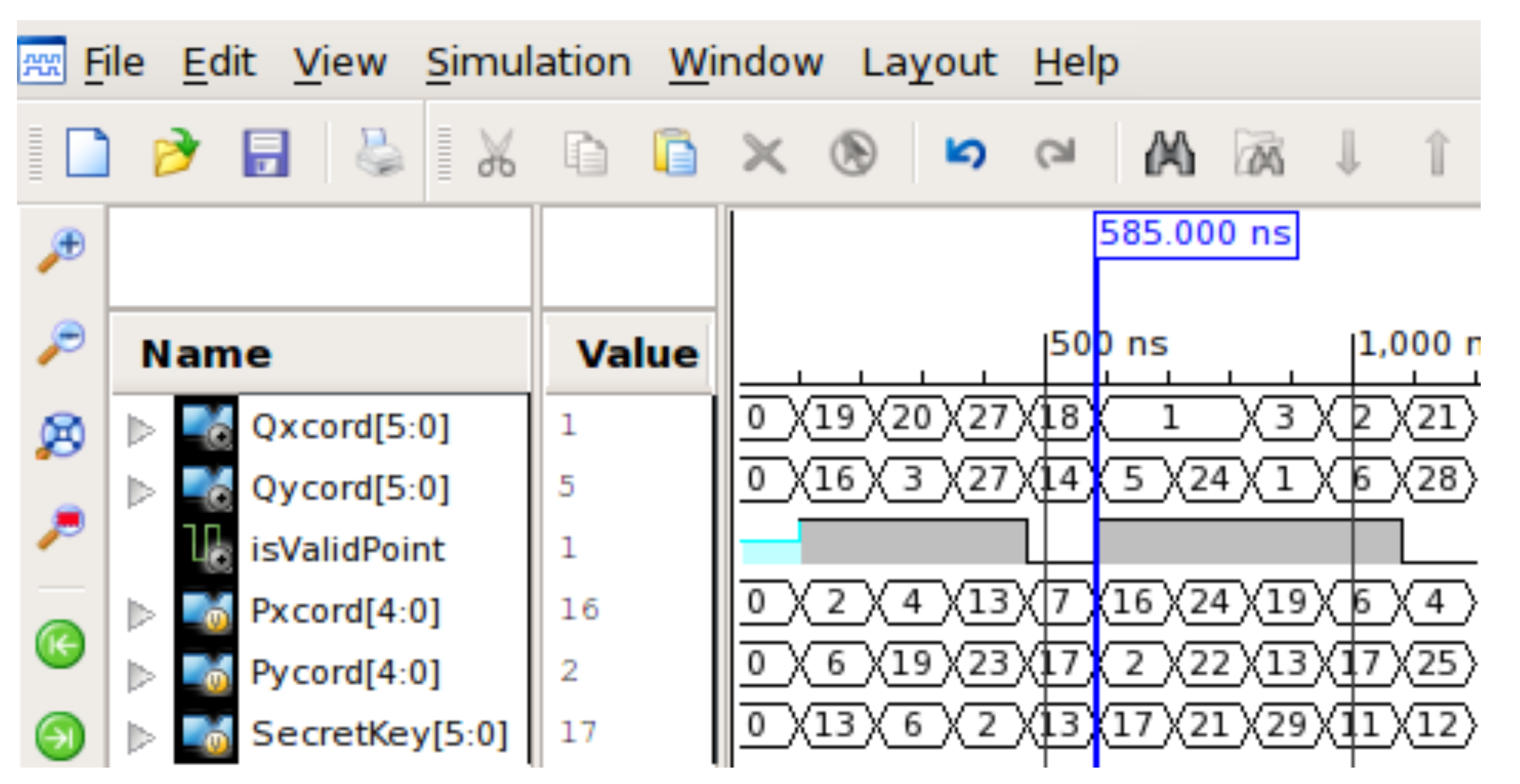
Figure 10 shows the simulation waveform for 9 random sample inputs among which two of the samples are illegal. The evolved circuit can correctly perform the elliptic curve scalar multiplication between a 6-bit secret key and a valid base point in the elliptic curve. If the base point is invalid, then a wrapper combinational circuit built around the evolved combinational circuit flags the output as invalid. This is marked by vertical line at simulation time
ns in
Figure 10.
Functional Verification of Asynchronous Circuit:Figure 5 shows the high-level circuit diagram of
circuit for elliptic curve scalar multiplication. The detailed internal architecture of elliptic curve scalar multiplication circuit is shown in
Figure 6. This circuit is implemented in VHDL and simulated with ISIM simulator. VHDL package is used to define the threshold gates and dual-rail signals. The simulation controller shown in
Figure 5 generates the random binary input samples for testing the scalar multiplication circuit. The simulation controller has a single-rail to dual-rail converter module that converts random binary samples into dual-rail signals. The output acknowledgement signal,
, from the scalar multiplication circuit controls the internal modules of the simulation controller.
Figure 11 shows the waveform of
circuit performing scalar multiplication. In dual-rail logic, the 6-bit secret-key is represented by 12-bit dual-rail signals, and the 5-bit base point value is represented by 10-bit dual-rail signals. In addition, two samples are separated by an all-one-spacer or all-zero-spacer. The alteration between various input/output DATA and two spacers are clearly shown in simulation (refer
Figure 11). To represent a single-rail signal (say Pxcord[4:0]) in
Figure 10) in dual-rail format, we created two signals (Pxcord_rail0[4:0] and Pxcord_rail1[4:0] in
Figure 11). The rail1 signal holds the exact value of a single-rail signal, and the rail0 signal holds the one’s complement of the single-rail signal. If Pxcord[4:0] is 2 (or
), then Pxcord_rail1 is 2 (or
) and Pxcord_rail0 is 29 (or
). Therefore, if we monitor the value of rail1 signals in
Figure 11, then we can compare them with the corresponding values in
Figure 10 to verify the functional correctness of our
circuit. The comparison of single-rail and dual-rail outputs using the same input values verifies that
is functionally correct. If we compare
Figure 10 and
Figure 11 using the same input values, then it is apparent that
is functionally correct.
Propagation Delay, Circuit Size, and Energy Consumption Profile: Although
circuits provide enhanced resilience against SCAs (
Section 7), they incur propagation delay, circuit size, and energy overheads as compared to the baseline circuits (i.e., same combinational circuits without using
). Consequently, we quantify propagation delay, circuit size, and energy consumption of the baseline circuits (here evolved
combinational circuits for point addition, point-doubling, and scalar multiplication) and
circuits.
Table 5 shows the values of propagation delay, circuit size, and energy consumption profile of the evolved
combinational circuits for elliptic curve point addition (ECPA), point-doubling (ECPD), and scalar multiplication (ECSM). The size and propagation delay of the evolved circuit are computed using the concept of gate equivalent [
39], which is a basic unit of measure for digital circuit complexity. The circuit size value in
Table 5 shows the factor by which the circuit is bigger than a NOT gate. For example, ECPA has circuit size of 237, which means it requires
more circuit area than a typical NOT gate. Results in
Table 5 reveal that we can employ a genetic algorithm to generate combinational circuits for an elliptic curve arithmetic. The interesting observation is that all the three circuits (for ECPA, ECPD, and ECSM) have
circuit configuration, which means each of the three circuits is made up of 160-logic gates. These three circuits have comparable propagation delay and energy consumption. This is essential to thwart simple power and timing analysis attack which is based on the timing differences in different point operation executions.
Table 6 shows the delay, size, and energy data for the delay-insensitive clock-free
circuits which are created by transforming the
combinational circuits generated by our genetic algorithm.
circuit requires input and output registrations, early completion detection circuitry, interaction of handshaking signals between adjacent register stages, and dual-rail representation of a single bit of data for correct functional operation. This introduces significant overhead in terms of propagation delay, circuit size, and energy consumption. Obviously,
circuits have delay, size, and energy overheads as compared to the baseline circuits.
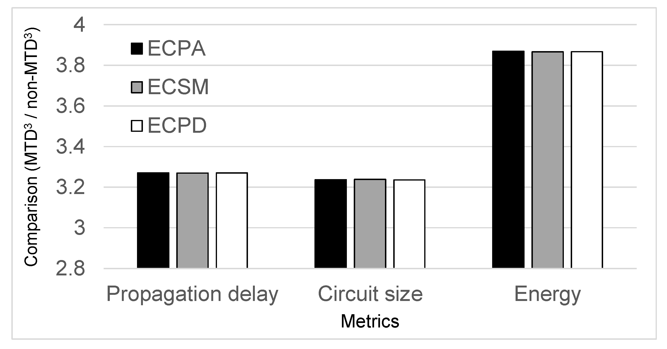
Figure 12 summarizes overheads of the
circuit implementation using
design approach over the same evolved circuit without
circuits. Results indicate that
design leads to 3.27×, 3.24×, and 3.87× higher propagation delay, circuit size, and energy, respectively, as compare to the non-
design. Thus, it is evident that
-based circuits have more overhead with respect to pure combinational circuits that do not use
. However, these costs come with the advantages of nearly constant power consumption during operation, low noise and electromagnetic emanations, which provide enhanced resilience against SCAs. Nevertheless, the overhead of our secure design is much lesser than some prior secure designs [
50], that is, 3× for our secure design versus 6× for some prior secure designs [
50]. We note that designing
circuits that incur minimum propagation delay, circuit size, and energy overheads as compared to the baseline circuits is a challenging endeavor. As process technology advances, we believe the overheads of
will be reduced due to the improved transistor device performance and energy efficiency. An efficient trade-off between the security and overhead (e.g., in terms of delay, area, and power) is an important research topic, though we leave thorough investigations on this trade-off as our future work.


