
A Standard-Cell-Based CMFB for Fully Synthesizable OTAs


Department of Information and Communication Technologies, Sapienza University of Rome, 00184 Rome, Italy
*
Author to whom correspondence should be addressed.
J. Low Power Electron. Appl. 2022, 12(2), 27; https://doi.org/10.3390/jlpea12020027
Submission received: 28 February 2022
/
Revised: 26 April 2022
/
Accepted: 27 April 2022
/
Published: 5 May 2022
(This article belongs to the Special Issue Ultra-Low-Power ICs for the Internet of Things)
Abstract
:In this paper, we propose a fully standard-cell-based common-mode feedback (CMFB) loop with an explicit voltage reference to improve the CMRR of pseudo-differential standard-cell-based amplifiers and to stabilize the dc output voltage. This latter feature allows robust biasing of operational transconductance amplifiers (OTAs) based on a cascade of such stages. A detailed analysis of the CMFB is reported to both provide insight into circuit behavior and to derive useful design guidelines. The proposed CMFB is then exploited to build a fully standard-cell OTA suitable for automatic place and route. Simulation results referring to the standard-cell library of a commercial 130 nm CMOS process illustrated a differential gain of 28.3 dB with a gain-bandwidth product of 15.4 MHz when driving a 1.5 pF load capacitance. The OTA exhibits good robustness under PVT and mismatch variations and achieves state-of-the-art FOMs also thanks to the limited area footprint.
1. Introduction
Recent years have seen a growing interest in ultra-low-voltage operational transconductance amplifiers (OTAs) [1,2,3,4,5,6,7,8,9,10,11,12,13,14,15,16,17,18] that are a key building block in many analog and mixed-signal applications such as Internet-of-Things (IoT) and biomedical ones [19,20,21,22]. This is a strong incentive to innovate the design flow of analog blocks: even if they often constitute just a small fraction of a mixed-signal system, their design requires a large fraction of the overall effort. Indeed, both the schematic and layout design are typically carried out manually, iterating each step several times until specifications are met, also taking into account the required robustness under process, supply voltage and temperature (PVT) variations. To minimize the analog design effort and hence the cost and time-to-market of such mixed-signal applications, circuit solutions for analog blocks based on digital standard cells were explored in [23,24]. The end goal is to achieve a fully automatic design flow for the analog blocks that is similar to the one adopted for the digital section; as an intermediate step, the use of digital standard cells to design analog functions allows for the automating of the place and route steps of the design flow and, in perspective, the achievement of a fully automatic synthesis flow for both analog and digital blocks.
Recently, different approaches to exploit digital-based architectures to mimic the behavior of analog functions were explored in [25]. In particular, the behavior of OTAs has been mimicked through VCO-based architectures [26,27,28] and the DIGOTA approach [29,30,31]. Even if all these innovative techniques are very interesting from a research point of view, the most common approach to implementing analog building blocks suitable for automatic place and route exploits the digital standard cells as basic analog amplifiers [32,33,34,35,36,37]. In fact, the simplest digital gate (the inverter) behaves as a common source amplifier [38], and several inverter-based OTAs [39,40,41,42,43,44,45,46,47,48,49,50] have been proposed in the literature. However, differently from custom-designed inverters, the standard-cell inverter is typically optimized for area footprint or symmetrical slew rate, and as a consequence, it exhibits a systematic offset in its input–output dc transfer characteristic which impacts the output static voltage and strongly degrades the performance of standard-cell-based cascaded amplifiers. According to the above considerations, the design of standard-cell-based OTAs must cope with additional issues that make achieving good and robust performance a very critical task. Several authors [37,42,50,51,52] have pointed out that the performances and even the operation of standard-cell-based analog circuits are severely impaired by PVT and mismatch variations, resulting in incorrect bias, large offsets and significant performance variations.
In such a context, the use of a common-mode feedback (CMFB) loop for each differential gain stage becomes mandatory to ensure a stable bias point [53,54,55], especially for ultra-low-voltage applications. The need to design a standard-cell-based CMFB greatly restricts the design options; some CMFB solutions have been proposed in the literature, but they usually do not involve an explicit reference voltage, resulting in some sensitivity to process, supply voltage and temperature (PVT) variations.
In this paper, we propose a fully standard-cell-based CMFB loop that exploits an explicit reference voltage to guarantee robust biasing, and we exploit it to design a two-stage OTA. Thanks to the proposed approach, a stable dc output voltage is guaranteed for the first stage, allowing a correct biasing of the second stage. The paper is structured as follows: in Section 2, the proposed CMFB is described and analyzed; in Section 3, the design of the standard-cell-based OTA is presented. Section 4 reports the simulation results, and, finally, conclusions are drawn in Section 5.
2. The Proposed CMFB
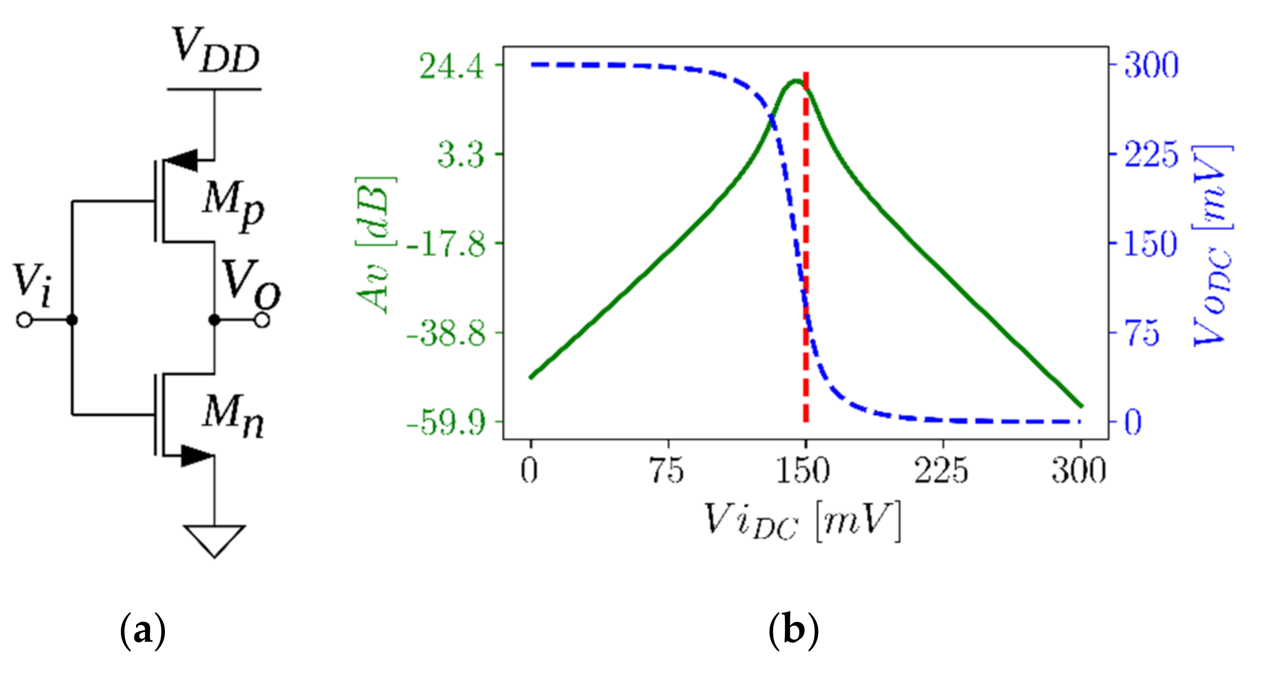
Figure 1a shows a CMOS inverter that can be thought of as a common-source amplifier. Its dc output voltage depends on the size of NMOS and PMOS devices and is also affected by PVT and mismatch variations. Figure 1b shows the dc input–output transfer characteristic (blue dashed line) and its derivative (continuous green line) for a typical standard-cell inverter, as a function of the input bias voltage Vi for a supply voltage VDD = 0.3 V. Figure 1b clearly shows that an incorrect input dc bias results in a drop of voltage gain, thus making multistage amplifiers very difficult to implement if the dc output voltage of basic inverter stages is not controlled. The plot in Figure 1b also highlights the systematic offset of the inverter from a standard-cell library. In fact, the maximum gain is achieved for an input bias voltage different from VDD/2 = 150 mV (value marked as a red dashed line). This systematic offset of the inverter (resulting in a logic threshold different from VDD/2) is due to the fact that standard cells are not optimized for analog applications, and a trade-off between area, propagation time and balancing constraints is considered.
A fully differential amplifier can be easily obtained using two inverters; however, it requires a CMFB loop to reduce the common-mode gain and to control the dc output voltage. Furthermore, to ensure correct biasing, multi-stage fully differential amplifiers require a CMFB at each stage. In the absence of accessible terminals to set the bias point of the inverter (e.g., the gate or body terminals of individual devices), the CMFB typically exploits two inverters with shorted outputs to sense the common-mode output voltage and other inverters as current sources to close the loop at the input of the main amplifier [53,54,55]. However, when applied to the first stage, this technique adds a resistive component to the input impedance of the OTA, and, therefore, the use of common-mode feedforward [33] has been proposed as an alternative. It is worth noting that, typically, this approach is used to reduce the common-mode gain, whereas other techniques such as body biasing [34,53] are exploited to set the output dc common-mode voltage. However, ultra-low voltage applications show low tolerance to biasing errors, and when standard-cell inverters are used, the body terminal is often not available for biasing purposes.
To maintain the advantages of the feedback avoiding this drawback, one option is to use a local common-mode feedback (LCMFB): when applied at transistor level [17], the LCMFB is typically implemented with a pair of common-mode sensing resistors whose central node is connected to the gates of the active load devices. The corresponding standard cell implementation [37] exploits a pair of sensing inverters and a pair of controlling inverters connected to the same output nodes. For the differential mode signal, the load impedance of the LCMFB is the output resistance of the loading inverters, whereas for the common-mode signal the LCMFB provides a low impedance load that reduces the gain, improving the common-mode rejection ratio (CMRR).
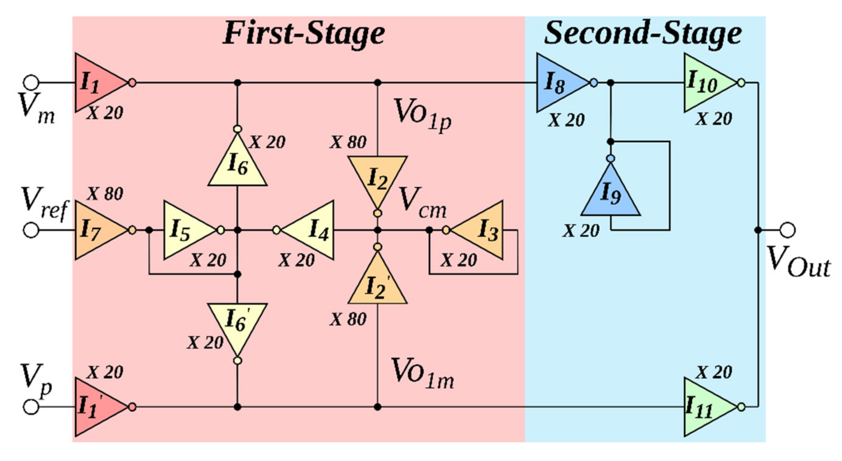
In this work, in order to improve the robustness of the dc operating point to PVT variations and to overcome the systematic offset of the standard cell inverters, we propose to add an explicit voltage reference Vref to the standard-cell LCMFB through the inverter I7, as shown in Figure 2.
The resulting fully differential amplifier topology is depicted in Figure 2 (indicated as First-Stage): different colors are used to highlight the inverters constituting the gain stage (I1 and I1’), the common-mode estimator (I2, I2’ and I3), the reference inverting buffer (I7, loaded by I5) and the CMFB auxiliary amplifier (I4, I5, I6 and I6’). Inverters with their input and output terminals connected together are used as load devices to avoid high impedance nodes in the loop, providing better stability and a degree of freedom to design the circuit, as will be shown following this section. They are equivalent to parallel NMOS and PMOS diode-connected devices; thus, the cascade of an inverter and such a diode-connected inverter is equivalent to the parallel connection of an NMOS and a PMOS diode-loaded common-source stage.
To analyze the proposed topology and obtain design guidelines, we model each inverter IX (X = 1, …, 7) with a transconductance gain GX and an output conductance GoX, given by
where gm and gds are the small-signal transconductance and output conductance of MOS devices, and n and p subscripts refer to NMOS and PMOS transistors, respectively. We assume that they scale linearly with the size of the devices (hence with the strength of the standard cells, IV_xN meaning an inverter whose devices have N times the minimum width), and their ratio is the voltage gain AX = GX/GoX that we assume is identical for all the inverters (hence AX = A for x = 1, …, 7).
Let α be the ratio of the strengths of inverters I6 and I1 (hence α = G6/G1), λ = G2/G3, ρ = G4/G5 and β = G7/G4. The differential voltage gain of the first stage in Figure 2 results in
where the loading effect of the LCMFB is considered. For the common mode, the analysis provides
where Vic and Voc are the input and output common-mode components. The gains are
where the error factors
take into account the effect of the output conductances (ideally, if GX >> GoX,, since A approaches to infinite, the values of and tend to 1).
Equations (3)–(9) show that the CMRR of the stage is set by in (7) and allow the ability to derive design guidelines for the choice of the inverter sizes. A trade-off between high CMRR and low gain penalty due to the loading effect involves the factor α: a large value of α maximizes the CMRR, whereas the smaller its value, the lower the reduction of the differential gain (3). A suitable solution is to choose α = 1 and maximize the CMRR acting on the other factors.
Correct biasing would require AR = 1, which in the limit of large CMRR implies
CMRR optimization then requires maximizing
that asymptotically tends to A for increasing β and ρ. Moreover, by (7) and the condition (10), we obtain
that poses the further design constraints. Equation (11) implies that the size of inverter I7 must be maximized, and (12) requires β < A.
In practical situations, the smallest inverter size to be used is limited by matching constraints (the smaller the transistors, the higher the standard deviation of mismatches, hence offset and common mode to differential mode conversion), and the largest inverter size is limited by area and power constraints and by available standard-cells. Hence, there is a limit to the size of I7 (that is βρ times larger than I5) and I2 (that is λ times larger than I3):
It must also be noted that there is a trade-off between CMRR and the common-mode range: a large value of λ provides a larger CMRR at the cost of the common-mode voltage swing at the output of the stage, since the output of I2 saturates.
From (12), setting a maximum value of λ poses a more stringent limit on the value of β:
If βmax > Rmax, βρ is set to Rmax and maximizing (11) requires keeping the factor ρ as small as possible (ρ = 1). If βmax < Rmax, which is the case for low values of the gain A, β = βmax must be chosen; (11) then becomes
and its optimization involves maximizing ρ, whose maximum value is set by (13) to Rmax/βmax. A flow graph illustrating this design procedure is reported in Figure 3.
Further insight into the behavior of the differential stage with the proposed CMFB can be gained by adding to the model of each inverter a current source IoffX that accounts for the offset of the inverter, i.e., the error in the output voltage with respect to VDD/2 when the input voltage is VDD/2:
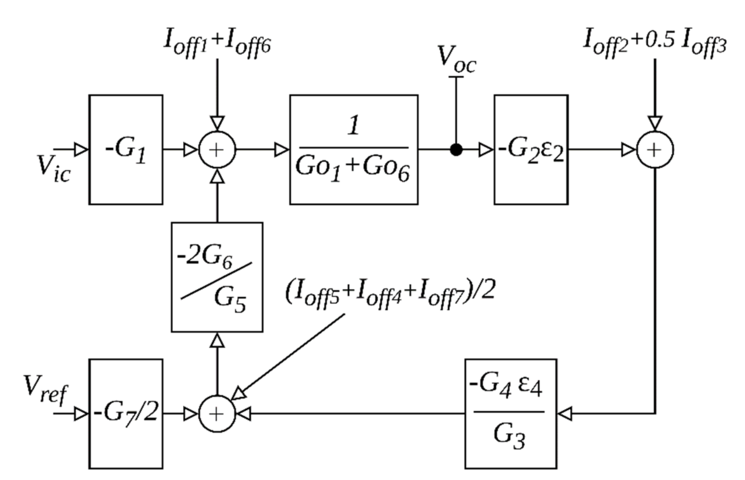
This current source accounts for both the systematic offset due to the design of the inverter (PMOS to NMOS size ratio) and the random variation due to mismatches, and we can assume it is proportional to the strength of the inverter. The resulting block scheme for the common-mode behavior of the stage is shown in Figure 4; if we consider the contribution to the output common-mode voltage Voc due to these offset current sources, which can be obtained by letting Vic = Vref = 0 in Figure 4, we obtain
Equation (17) shows that the residual error on setting Voc = Vref is due also to the offset currents of the inverters and that the CMFB suppresses this error in the limit of its finite loop gain. This is true both for the systematic offset currents and for their random components, thus demonstrating that the circuit provides a stable dc output voltage under process and mismatch variations. It must be noted that a suitable choice of the inverter strengths can lead to minimizing (17) and could be used as a further design constraint for design optimization.
3. Standard-Cell-Based OTA
An operational transconductance amplifier must provide high voltage gain, thus requiring, especially in an ultra-low-voltage environment with deep submicron technologies, the cascade of at least two gain stages with a differential-to-single-ended (D2S) conversion.
In the context of a standard-cell-based approach, mimicking the typical analog architecture with an input D2S converter followed by single-ended gain stages would result in a very poor CMRR and in a very high sensitivity to PVT variations. Better performance can be achieved by exploiting differential stages with CMFB loops to improve the CMRR and stabilize the bias point, followed by a final D2S stage.
To illustrate this approach, we propose a two-stage OTA, shown in Figure 2, composed by the fully differential stage described in the previous section (First-Stage) followed by a standard-cell-based D2S converter (Second-Stage), composed by inverters I8–I11. Inverters I8 and I9 constitute an inverting voltage buffer whose gain is ideally −1, and inverters I10 and I11 act as transconductance amplifiers driving the same output node.
The voltage gain of the D2S stage is thus ideally
with an infinite CMRR. However, in deep submicron technologies the voltage gain A is limited; hence, the output conductances of I8 and I9 cannot be neglected in the analysis. This reduces the gain of the voltage buffer and drastically worsens the CMRR even in typical conditions. Assuming I8 = I9 and I10 = I11, differential and common-mode gains of the second stage are
and the overall CMRR results are
where D, defined in (7), is the CMRR of the first stage.
The D2S stage presents an output pole set by the load capacitance CL; moreover, its dual path nature results in a pole–zero doublet similar to that provided by the current mirror load of a differential pair. With reference to Figure 2, assuming I8 = I9 and I10 = I11 and considering a differential input to the D2S (i.e., Vo1p = −Vo1m), the frequency response of the D2S can be written as
where CX is the total capacitance seen at the output of I8. Equation (22) shows that the pole and zero due to the inverting buffer I8–I9 are spaced by an octave; thus, their effect can be neglected. It must further be noted that Equation (22) poses no constraint on the sizing of inverters I8 and I9 with respect to I10 and I11; regardless, it could be convenient to use inverters of the same size to provide a symmetric loading to the first stage.
The OTA is stable when driving a sufficiently large load capacitance that makes the output pole dominant; for small load capacitors, a compensation is needed. More in detail, neglecting the pole–zero doublet due to I8 and I9, the internal pole of the OTA is given by
where Cin2 and Cin8 are the input capacitances of I2 and I8, and the output pole is
(assuming I10 = I11). By imposing that the second pole is γ times the unity-gain frequency (where γ is set by the required phase margin), the minimum load capacitance required to have stability with the dominant pole at the output is
where α = 1 has been considered. Equation (25) shows that the standard-cell-based OTA has the capacity to drive small capacitors, as required in most on-chip applications, without the need of compensation capacitors thanks to the fact that the intrinsic gain of inverters is low and small-size inverters are used in the output stage. The latter condition, however, limits the slew rate of the OTA.
4. Simulation Results
The OTA in Figure 2 was designed using the standard-cell library of the STMicroelectronics 130 nm CMOS technology. Supply voltage was set to 0.3 V. Taking into account the design guidelines in Section 2 and the mismatch requirements that impose the use of non-minimum size cells, the inverters were designed as specified in Figure 2 (inverter IV_xN has devices with N times the minimum width). It must be noted that the low voltage gain of the inverters (A = 19 dB) result in the error factors (8) and (9) that are significantly below 1: in particular, we obtain and With reference to the analysis in Section 2, the smallest inverters were chosen as 20 times the minimum size inverter (IV_x20 for all the inverters except I2 and I8) and the design factors were set to α = 1, λ = 4, ρ = 1 and β = 4. The resulting static offset is therefore
To assess the effectiveness of the proposed approach in stabilizing the dc output voltage, the pseudo-differential stage with the CMFB was tested under PVT variations. The reference voltage was set to VDD/2, and the error of the output dc common-mode voltage with respect to this reference was evaluated. The LCMFB without I7 and the reference input were also tested for comparison.
Figure 5 shows the relative error on the dc output common-mode voltage for the proposed CMFB and for the LCMFB without the reference input, under variations of temperature and supply voltage. An error is present in typical conditions (300 mV VDD, 27 °C) due to the finite loop gain of the CMFB. When the reference input is present, the output common-mode voltage presents a limited variation when the temperature ranges from 0° to 80 °C, whereas the voltage drifts with the temperature if the reference input is not used. For what concerns the variation of the supply voltage, the dc common-mode output voltage tracks VDD/2 with an error, due to the finite loop gain, that presents little variation and is lower than the error achieved by the design without the reference input.
The advantage provided by the reference input is even more evident when the effect of process variations is considered. Figure 6 shows the relative error on the dc output common-mode voltage with respect to the reference input for the extreme process corners. A residual error of about 1.34% is reported in typical (TT) conditions due to the finite loop gain of the CMFB. This error increases in the corners where NMOS and PMOS devices present opposite variations (corners FS and SF); however, the values are below 10% and are one third of the errors obtained if the reference input is not used.
The proposed pseudo-differential stage with CMFB thus results in suitable-to-design multi-stage amplifiers, and the OTA in Figure 2 was designed and simulated. The amplifier dissipates 4.4 μW from a 0.3 V supply; this relatively high power consumption is due to the use of large inverters to minimize the mismatches. Figure 7 shows the differential (AVD) and common-mode (AVC) gains of the OTA loaded by a 1.5 pF capacitor. The differential dc gain is 28.27 dB with a 15.42 MHz unity-gain frequency and 54.18° phase margin; the common-mode rejection ratio (CMRR) is about 41.07 dB and is constant across all the bandwidth.
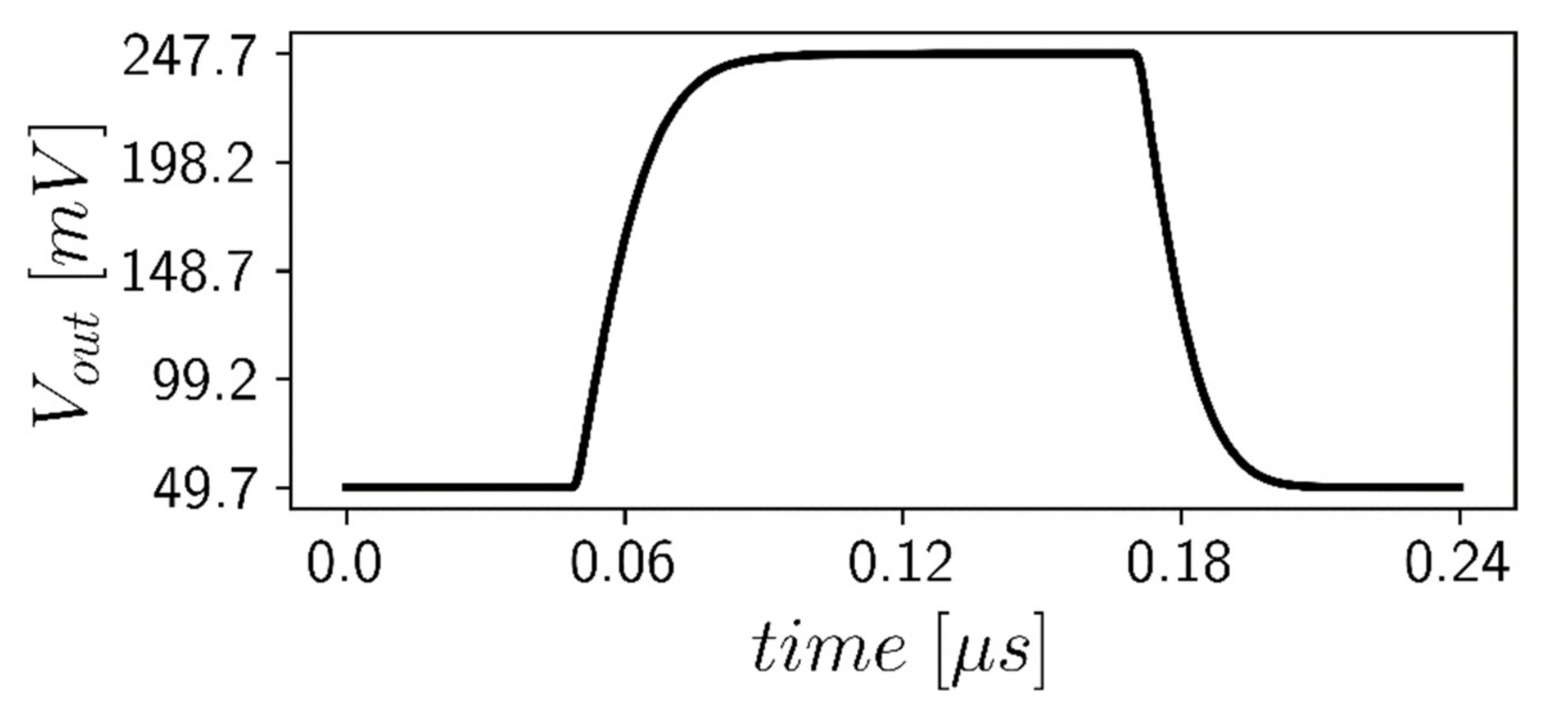
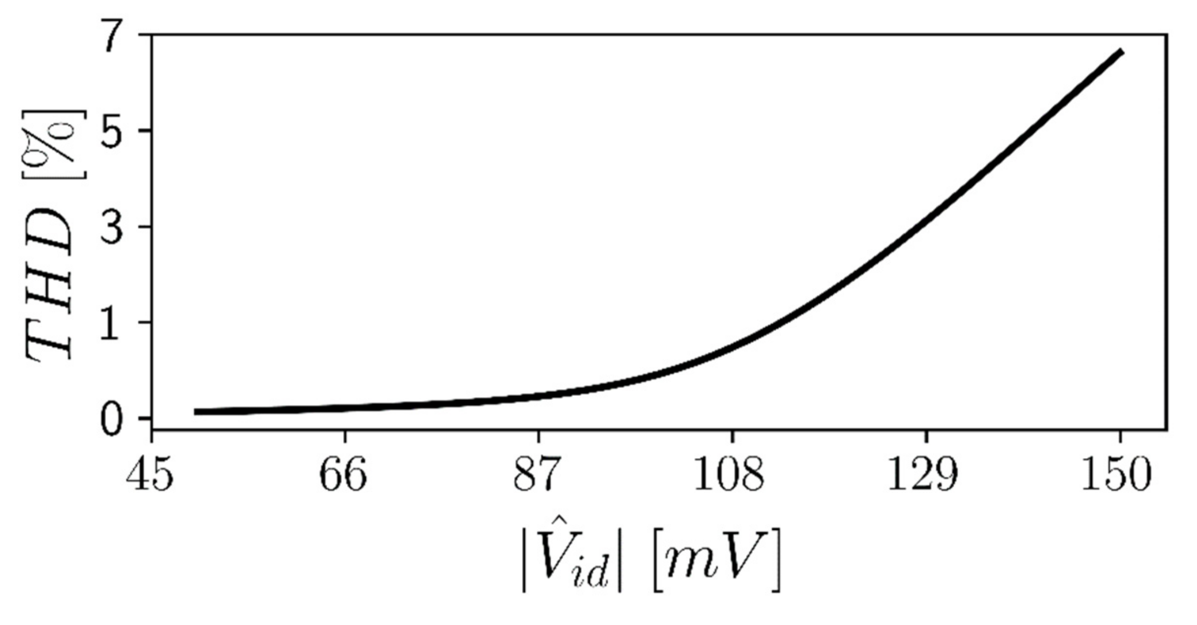
The amplifier was tested in a unity-gain buffer configuration to assess its large-signal performance. The response to an input pulse from 45 to 255 mV (Figure 8) shows identical values for positive and negative slew rates equal to 9.75 V/μs. We also simulated the unity-gain buffer configuration with a 1 MHz sinusoidal input applied, and Figure 9 reports the total harmonic distortion (THD) as a function of the input amplitude. Distortions below 1% (−40 dB THD) are obtained for an input amplitude up to 115 mV, which is about 75% of the rail-to-rail swing.
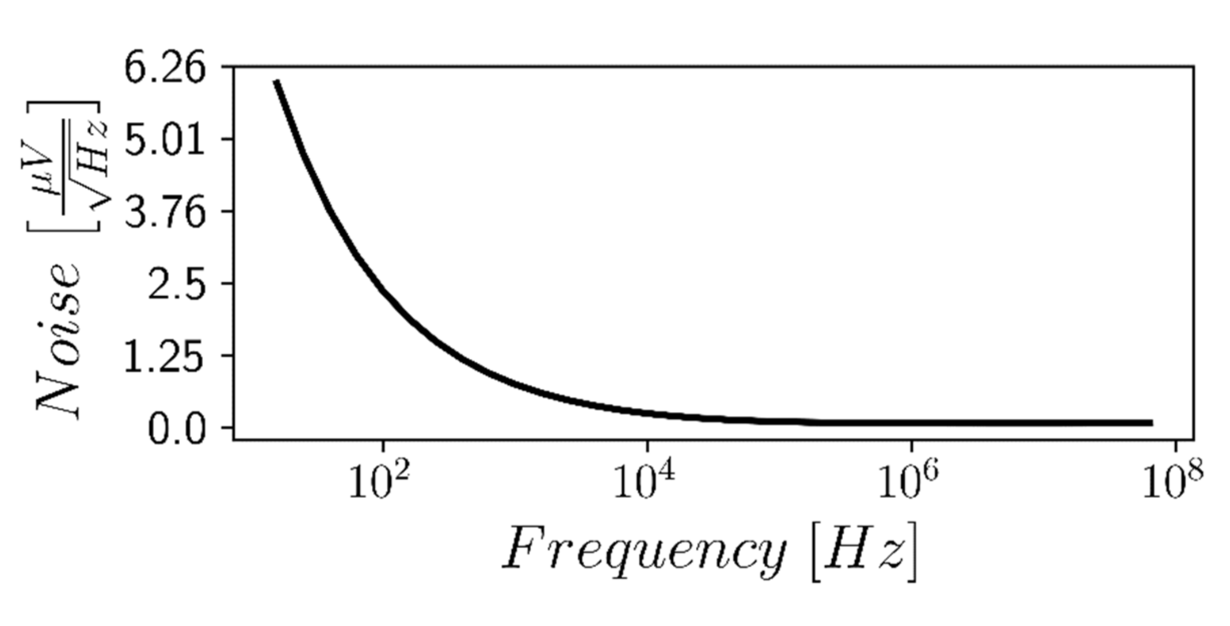
Figure 10 shows the input-referred noise spectrum of the OTA: a noise corner frequency lower than 1 kHz with a white noise spectral density of 0.497μV/√Hz measured at 10 kHz was obtained, resulting in 1.445 mV rms noise when integrated over the whole closed-loop bandwidth.
The performance under PVT variations and mismatches was evaluated to assess the robustness of the design. Table 1 reports the main performance parameters of the OTA in five different process corners highlighting how the proposed circuit exhibits a relatively low sensitivity to process variations. The effect of supply voltage and temperature variations is reported in Table 2: power consumption and gain-bandwidth product exhibit a non-negligible variation as expected since there is no bias loop setting the currents. However, the voltage gain AVD and the output dc voltage (measured through the parameter VOS) are extremely stable, confirming the effectiveness of the proposed approach.
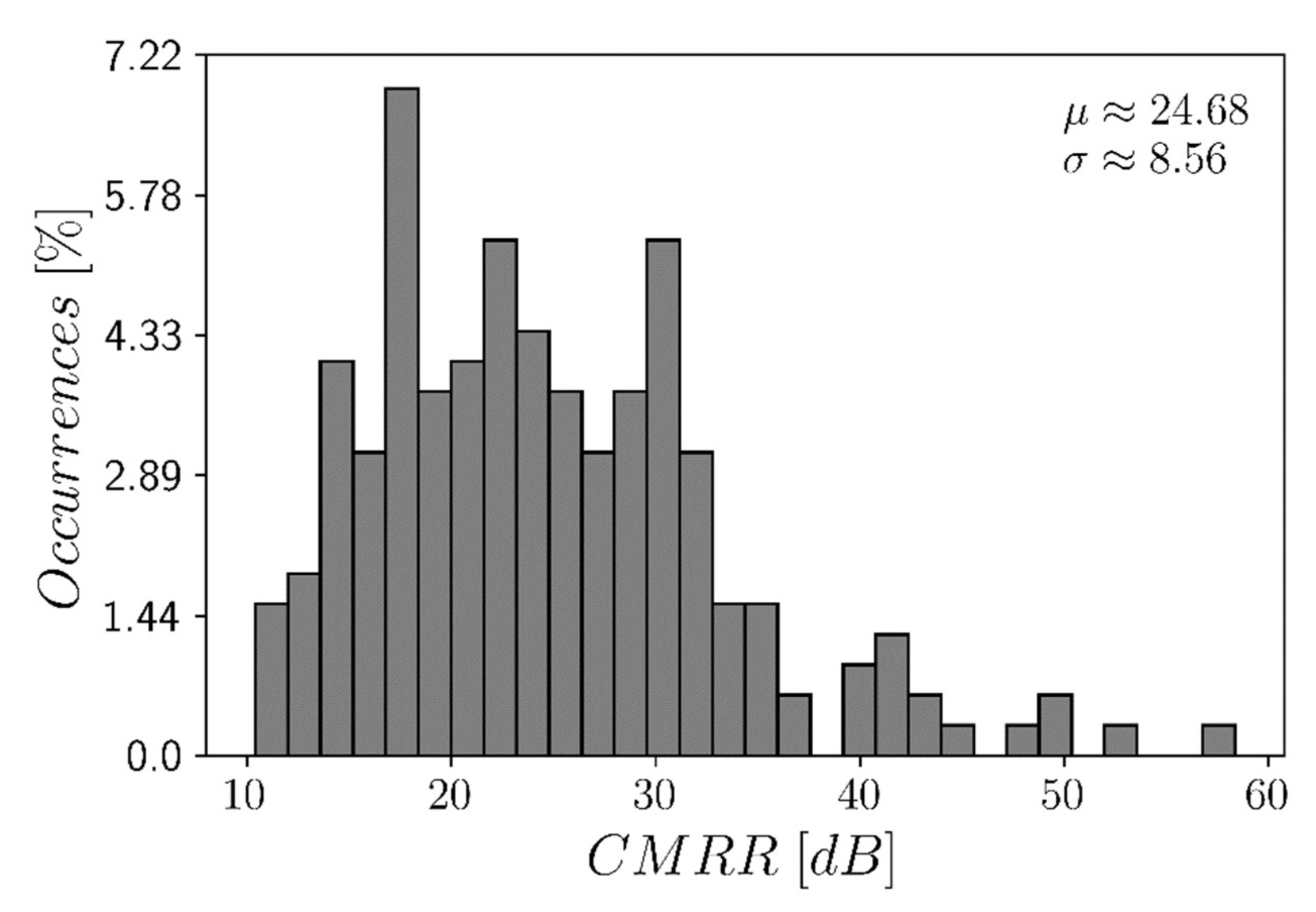
Table 3 reports the results of 200 Monte Carlo mismatch simulations that show a good robustness of the proposed OTA, with limited variation of all the parameters. As can be observed in Table 3, under mismatch variations, the standard deviation of the output offset voltage is 9.2 mV, in line with other ULV OTAs taken from the literature. In order to further reduce the standard deviation of VOS under mismatch variations, we can place multiple gates in parallel or exploit standard cells with larger driving capability, at the cost, however, of increased area and power consumption. We consider the proposed design as a good tradeoff between area, power consumption and output offset voltage standard deviation. Figure 11 shows the histogram of the CMRR, which is always higher than 10 dB and presents a log-normal distribution. The histogram shows that, even under mismatch conditions, acceptable values of CMRR are obtained, taking also into account the low value of the differential gain.
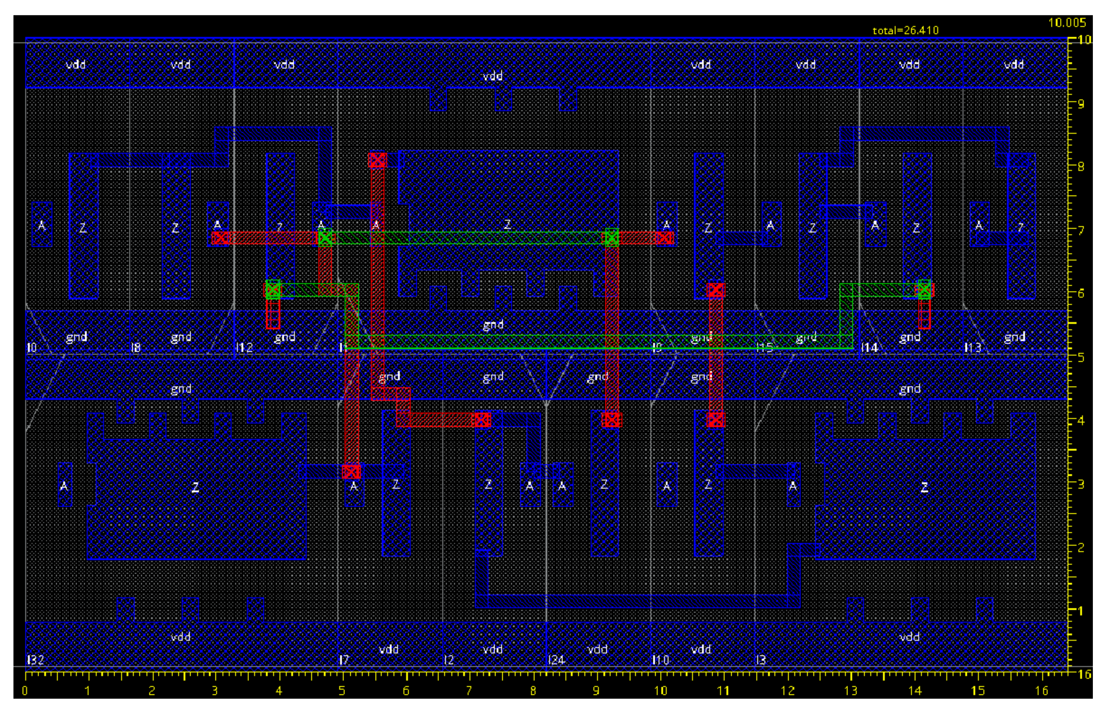
The layout of the proposed standard-cell OTA was generated by means of an automatic place and route flow by using the Cadence Innovus tool and is shown in Figure 12. The OTA occupies an area of 16.4 × 10 μm2 that is very limited, notwithstanding the use of large inverters to minimize the mismatches. The layout has been generated automatically starting from a Verilog netlist of the circuit, which is reported in the Appendix A.
Table 4 reports the comparison of the proposed OTA with other ULV OTAs from the literature. To compare the proposed OTA against state-of-the-art low-voltage amplifiers, we refer to the following commonly used figures of merit:
where GBW is the gain-bandwidth product, CL the load capacitance, SRAVG is the average slew rate and Pd is the power consumption. Subscripts S and L in (27) and (28) denote small signal and large signal, respectively, while the figures of merit (29) and (30) are normalized with respect to the layout area of the OTA. The comparison shows that the proposed circuit exhibits very good small signal performance and adequate large signal performance. Due to the very compact layout, the proposed OTA outperforms all other similar designs in terms of . The proposed OTA also outperforms almost all other designs in terms of . Only [30] exhibits a higher ; however, the OTA in [30] is made up of minimum-sized standard cells that result in high sensitivity to process variations and mismatches.
5. Conclusions
In this paper, we have presented a fully standard-cell-based common-mode feedback (CMFB) loop with an explicit voltage reference that allows the improvement of the CMRR of fully synthesizable standard-cell-based amplifiers and the stabilization of the dc output voltage with respect to PVT variations. A complete analysis of the circuit was presented to derive design guidelines. Simulations displayed that the use of an explicit reference input enhances the robustness of the CMFB to PVT variations.
The proposed CMFB was exploited to design a standard-cell-based OTA made up of only digital gates taken from a standard-cell library. The layout of the OTA was implemented by using a fully automated place and route flow by using the Cadence Innovus tool and starting from the Verilog netlist of the circuit. Simulation results illustrated very good values of both the small signal and large signal FOMs normalized to the area footprint of the circuits with a very good robustness of all the main performance parameters to PVT variations.
We remark that, due to the adoption of the proposed CMFB and to the design equations derived in this paper, the proposed standard-cell-based OTA results are more robust to PVT variations with respect to DIGITAL and standard-cell-based OTAs previously reported in the literature. However, it is worth noting that the performance attained by standard-cell-based OTAs is still less robust with respect to PVT and mismatch variations than that of OTAs designed with a custom analog design approach, which exhibit a well-defined bias current. Moreover, one of the main drawbacks of standard-cell single-ended OTAs is that the D2S converter (the last stage of the proposed OTA) cannot achieve good performance under PVT and mismatch variations, resulting in low and variable CMRR, thus reducing the ICMR of the whole architecture. Therefore, one of the goals of future works will be to achieve better ICMR and CMRR performance by standard-cell D2S converters in order to enhance the performance of standard-cell-based OTAs.
Author Contributions
Conceptualization, F.C., R.D.S. and G.S.; methodology, F.C., R.D.S. and G.S.; software, R.D.S.; validation, F.C., R.D.S. and G.S.; formal analysis, F.C. and R.D.S.; investigation, F.C., R.D.S. and G.S.; data curation, R.D.S.; writing—original draft preparation, F.C.; writing—review and editing, F.C., R.D.S. and G.S.; visualization, R.D.S.; supervision, F.C. and G.S. All authors have read and agreed to the published version of the manuscript.
Funding
This research received no external funding.
Conflicts of Interest
The authors declare no conflict of interest.
Appendix A
Verilog netlist of the proposed OTA is as follows:
‘timescale 1 ns/1 ns
module OTA (
inout REF,
inout Vim,
inout Vip,
inout Vout );
IV_X20 I24 ( .Z(feed), .A(CM));
IV_X20 I15 ( .Z(net8), .A(Vop1));
IV_X20 I14 ( .Z(Vout), .A(net8));
IV_X20 I13 ( .Z(net8), .A(net8));
IV_X20 I12 ( .Z(Vout), .A(Vom1));
IV_X20 I10 ( .Z(Vop1), .A(Vim));
IV_X20 I9 ( .Z(Vop1), .A(feed));
IV_X20 I8 ( .Z(Vom1), .A(feed));
IV_X20 I7 ( .Z(feed), .A(feed));
IV_X20 I2 ( .Z(CM), .A(CM));
IV_X20 I0 ( .Z(Vom1), .A(Vip));
IV_X80 I32 ( .Z(feed), .A(REF));
IV_X80 I3 ( .Z(CM), .A(Vop1));
IV_X80 I1 ( .Z(CM), .A(Vom1));
endmodule
References
- Chatterjee, S.; Tsividis, Y.; Kinget, P. 0.5-V analog circuit techniques and their application in OTA and filter design. IEEE J. Solid State Circuits 2005, 40, 2373–2387. [Google Scholar] [CrossRef]
- Ferreira, L.; Sonkusale, S.R. A 60-dB Gain OTA Operating at 0.25-V Power Supply in 130-nm Digital CMOS Process. IEEE Trans. Circuits Syst. I Regul. Pap. 2014, 61, 1609–1617. [Google Scholar] [CrossRef]
- Abdelfattah, O.; Roberts, G.W.; Shih, I.; Shih, Y.-C. An Ultra-Low-Voltage CMOS Process-Insensitive Self-Biased OTA with Rail-to-Rail Input Range. IEEE Trans. Circuits Syst. I Regul. Pap. 2015, 62, 2380–2390. [Google Scholar] [CrossRef]
- Akbari, M.; Hashemipour, O. A 63-dB gain OTA operating in subthreshold with 20-nW power consumption. Int. J. Circuit Theory Appl. 2017, 45, 843–850. [Google Scholar] [CrossRef]
- Richelli, A.; Colalongo, L.; Kovacs-Vajna, Z.; Calvetti, G.; Ferrari, D.; Finanzini, M.; Pinetti, S.; Prevosti, E.; Savoldelli, J.; Scarlassara, S. A Survey of Low Voltage and Low Power Amplifier Topologies. J. Low Power Electron. Appl. 2018, 8, 22. [Google Scholar] [CrossRef] [Green Version]
- Veldandi, H.; Shaik, R.A. A 0.3-V Pseudo-Differential Bulk-Input OTA for Low-Frequency Applications. Circuits Syst. Signal Process. 2018, 37, 5199–5221. [Google Scholar] [CrossRef]
- Grasso, A.D.; Pennisi, S. Ultra-Low Power Amplifiers for IoT Nodes. In Proceedings of the 2018 25th IEEE International Conference on Electronics, Circuits and Systems (ICECS), Bordeaux, France, 9–12 December 2018. [Google Scholar]
- Kulej, T.; Khateb, F. A Compact 0.3-V Class AB Bulk-Driven OTA. IEEE Trans. Very Large Scale Integr. Syst. 2020, 28, 224–232. [Google Scholar] [CrossRef]
- Renteria-Pinon, M.; Ramirez-Angulo, J.; Diaz-Sanchez, A. Simple Scheme for the Implementation of Low Voltage Fully Differential Amplifiers without Output Common-Mode Feedback Network. J. Low Power Electron. Appl. 2020, 10, 34. [Google Scholar] [CrossRef]
- Woo, K.-C.; Yang, B.-D. A 0.25V Rail-to-Rail Three-Stage OTA with an Enhanced DC Gain. IEEE Trans. Circuits Syst. II Express Briefs 2020, 67, 1179–1183. [Google Scholar] [CrossRef]
- Kulej, T.; Khateb, F. A 0.3-V 98-dB Rail-to-Rail OTA in 0.18 μ m CMOS. IEEE Access 2020, 8, 27459–27467. [Google Scholar] [CrossRef]
- Deo, N.; Sharan, T.; Dubey, T. Subthreshold biased enhanced bulk-driven double recycling current mirror OTA. Analog Integr. Circuits Signal Process. 2020, 105, 229–242. [Google Scholar] [CrossRef]
- Centurelli, F.; Sala, R.D.; Scotti, G.; Trifiletti, A. A 0.3 V, Rail-to-Rail, Ultralow-Power, Non-Tailed, Body-Driven, Sub-Threshold Amplifier. Appl. Sci. 2021, 11, 2528. [Google Scholar] [CrossRef]
- Centurelli, F.; Sala, R.D.; Monsurrò, P.; Scotti, G.; Trifiletti, A. A 0.3 V rail-to-rail ultra-low-power OTA with improved bandwidth and slew rate. J. Low Power Electron. Appl. 2021, 11, 19. [Google Scholar] [CrossRef]
- Dong, S.; Wang, Y.; Tong, X.; Wang, Y.; Liu, C. A 0.3-V 8.72-nW OTA with Bulk-Driven Low-Impedance Compensation for Ultra-Low Power Applications. Circuits Syst. Signal Process. 2021, 40, 2209–2227. [Google Scholar] [CrossRef]
- Ghosh, S.; Bhadauria, V. An ultra-low-power near rail-to-rail pseudo-differential subthreshold gate-driven OTA with improved small and large signal performances. Analog Integr. Circuits Signal Process. 2021, 109, 345–366. [Google Scholar] [CrossRef]
- Centurelli, F.; Sala, R.D.; Monsurrò, P.; Tommasino, P.; Trifiletti, A. An ultra-low-voltage class-AB OTA exploiting local CMFB and body-to-gate interface. AEU Int. J. Electron. Commun. 2022, 145, 154081. [Google Scholar] [CrossRef]
- Centurelli, F.; Sala, R.D.; Monsurrò, P.; Scotti, G.; Trifiletti, A. A tree-based architecture for high-performance ultra-low-voltage amplifiers. J. Low Power Electron. Appl. 2022, 12, 12. [Google Scholar] [CrossRef]
- Ng, K.A.; Xu, Y.P. A Low-Power, High CMRR Neural Amplifier System Employing CMOS Inverter-Based OTAs with CMFB Through Supply Rails. IEEE J. Solid State Circuits 2016, 51, 724–737. [Google Scholar]
- Giustolisi, G.; Palumbo, G. A gm/ID-based design strategy for IoT and ultra-low-power OTAs with fast-settling and large capacitive loads. J. Low Power Electron. Appl. 2021, 11, 21. [Google Scholar] [CrossRef]
- Silva, R.S.; Rodovalho, L.H.; Aiello, O.; Rodrigues, C.R. A 1.9 nW, Sub-1 V, 542 pA/V Linear Bulk-Driven OTA with 154 dB CMRR for Bio-Sensing Applications. J. Low Power Electron. Appl. 2021, 11, 40. [Google Scholar] [CrossRef]
- Vafaei, M.; Parhizgar, A.; Abiri, E.; Salehi, M.R. A low power and ultra-high input impedance analog front end based on fully differential difference inverter-based amplifier for biomedical applications. AEU Int. J. Electron. Commun. 2021, 142, 154005. [Google Scholar] [CrossRef]
- Newton, S.M.; Kinget, P.R. A 4th-order analog continuous-time filter designed using standard cells and automatic digital logic design tools. In Proceedings of the 2016 IEEE International Symposium on Circuits and Systems (ISCAS), Montreal, QC, Canada, 22–25 May 2016. [Google Scholar]
- Liu, J.; Park, B.; Guzman, M.; Fahmy, A.; Kim, T.; Maghari, N. A Fully Synthesized 77-dB SFDR Reprogrammable SRMC Filter Using Digital Standard Cells. IEEE Trans. Very Large Scale Integr. Syst. 2018, 26, 1126–1138. [Google Scholar] [CrossRef]
- Toledo, P.; Rubino, G.R.; Musolino, F.; Crovetti, P. Re-Thinking Analog Integrated Circuits in Digital Terms: A New Design Concept for the IoT Era. IEEE Trans. Circuits Syst. II Express Briefs 2021, 68, 816–822. [Google Scholar] [CrossRef]
- Drost, B.; Talegaonkar, M.; Hanumolu, P.K. Analog Filter Design Using Ring Oscillator Integrators. IEEE J. Solid State Circuits 2012, 47, 3120–3129. [Google Scholar] [CrossRef]
- Hsu, C.-W.; Kinget, P.R. A 40MHz 4th-order active-UGB-RC filter using VCO-based amplifiers with zero compensation. In Proceedings of the ESSCIRC 2014—40th European Solid State Circuits Conference (ESSCIRC), Venice, Italy, 22–26 September 2014; pp. 359–362. [Google Scholar]
- Kalani, S.; Bertolini, A.; Richelli, A.; Kinget, P.R. A 0.2V 492nW VCO-based OTA with 60 kHz UGB and 207 μVrms noise. In Proceedings of the 2017 IEEE International Symposium on Circuits and Systems (ISCAS), Baltimore, MD, USA, 28–31 May 2017. [Google Scholar]
- Crovetti, P. A Digital-Based Analog Differential Circuit. IEEE Trans. Circuits Syst. I Regul. Pap. 2013, 60, 3107–3116. [Google Scholar] [CrossRef]
- Palumbo, G.; Scotti, G. A Novel Standard-Cell-Based Implementation of the Digital OTA Suitable for Automatic Place and Route. J. Low Power Electron. Appl. 2021, 11, 42. [Google Scholar] [CrossRef]
- Toledo, P.; Crovetti, P.; Aiello, O.; Alioto, M. Design of Digital OTAs with Operation Down to 0.3 V and nW Power for Direct Harvesting. IEEE Trans. Circuits Syst. I Regul. Pap. 2021, 68, 3693–3706. [Google Scholar] [CrossRef]
- Nauta, B. A CMOS transconductance-C filter technique for very high frequencies. IEEE J. Solid-State Circuits 1992, 27, 142–153. [Google Scholar] [CrossRef] [Green Version]
- Barthélemy, H.; Meillère, S.; Gaubert, J.; Dehaese, N.; Bourdel, S. OTA based on CMOS inverters and application in the design of tunable bandpass filter. Analog Integr. Circuits Signal Process. 2008, 57, 169–178. [Google Scholar] [CrossRef]
- Vlassis, S. 0.5 V CMOS inverter-based tunable transconductor. Analog Integr. Circuits Signal Process. 2012, 72, 289–292. [Google Scholar] [CrossRef]
- Lv, L.; Zhou, X.; Qiao, Z.; Li, Q. Inverter-Based Subthreshold Amplifier Techniques and Their Application in 0.3-V ΔΣ-Modulators. IEEE J. Solid-State Circuits 2019, 54, 1436–1445. [Google Scholar] [CrossRef]
- Braga, R.A.S.; Ferreira, L.H.C.; Coletta, G.D.; Dutra, O.O. A 0.25-V calibration-less inverter-based OTA for low-frequency Gm-C applications. Microelectron. J. 2019, 83, 62–72. [Google Scholar] [CrossRef]
- Manfredini, G.; Catania, A.; Benvenuti, L.; Cicalini, M.; Piotto, M.; Bruschi, P. Ultra-Low-Voltage Inverter-Based Amplifier with Novel Common-Mode Stabilization Loop. Electronics 2020, 9, 1019. [Google Scholar] [CrossRef]
- Bae, W. CMOS Inverter as Analog Circuit: An Overview. J. Low Power Electron. Appl. 2019, 9, 26. [Google Scholar] [CrossRef] [Green Version]
- Michel, F.; Steyaert, M.S.J. A 250 mV 7.5 μW 61 dB SNDR SC ∆Σ modulator using near-threshold-voltage-biased inverter amplifiers in 130 nm CMOS. IEEE J. Solid State Circuits 2012, 47, 709–721. [Google Scholar] [CrossRef]
- Yang, Z.; Yao, L.; Lian, Y. A 0.5-V 35-μW 85-dB DR double-sampled ∆Σ modulator for audio applications. IEEE J. Solid State Circuits 2012, 47, 722–735. [Google Scholar] [CrossRef]
- Suadet, A.; Kasemsuwan, V. A CMOS inverter-based class-AB pseudo-differential amplifier with current-mode common-mode feedback (CMFB). Analog Integr. Circuits Signal Process. 2013, 74, 387–398. [Google Scholar] [CrossRef]
- Ismail, A.; Mostafa, I. A process-tolerant, low-voltage, inverter-based OTA for continuous-time Σ-∆ ADC. IEEE Trans. Very Large Scale Integr. Syst. 2016, 24, 2911–2917. [Google Scholar] [CrossRef]
- Yeknami, A.F. A 300-mV ∆Σ Modulator Using a Gain-Enhanced, Inverter-Based Amplifier for Medical Implant Devices. J. Low Power Electron. Appl. 2016, 6, 4. [Google Scholar] [CrossRef] [Green Version]
- De Aguirre, P.C.C.; Susin, A.A. PVT compensated inverter-based OTA for low-voltage CT sigma-delta modulators. Electron. Lett. 2018, 54, 1264–1266. [Google Scholar] [CrossRef]
- Baghtash, H.F. A 0.4 V, tail-less, fully differential trans-conductance amplifier: An all inverter-based structure. Analog Integr. Circuits Signal Process. 2020, 104, 1–15. [Google Scholar] [CrossRef]
- Rodovalho, L.; Aiello, O.; Rodrigues, C. Ultra-Low-Voltage Inverter-Based Operational Transconductance Amplifiers with Voltage Gain Enhancement by Improved Composite Transistors. Electronics 2020, 9, 1410. [Google Scholar] [CrossRef]
- Baghtash, H.F. Bias-stabilized inverter-amplifier: An inspiring solution for low-voltage and low-power applications. Analog Integr. Circuits Signal Process. 2020, 105, 243–248. [Google Scholar] [CrossRef]
- Rodovalho, L.H. Push-pull based operational transconductance amplifier topologies for ultra low voltage supplies. Analog Integr. Circuits Signal Process. 2021, 106, 111–124. [Google Scholar] [CrossRef]
- Lee, S.; Park, S.; Kim, Y.; Kim, Y.; Lee, J.; Lee, J.; Chae, Y. A 0.6-V 86.5-dB DR 40-kHz BW inverter-based continuous-time delta-sigma modulator with PVT-robust body-biasing. IEEE Solid State Circuits Lett. 2021, 4, 178–181. [Google Scholar] [CrossRef]
- Rodovalho, L.; Rodrigues, C.R.; Aiello, O. Self-Biased and Supply-Voltage Scalable Inverter-Based Operational Transconductance Amplifier with Improved Composite Transistors. Electronics 2021, 10, 935. [Google Scholar] [CrossRef]
- Baltolu, A.; Albinet, X.; Chalet, F.; Dallet, D.; Begueret, J.-B. A robust inverter-based amplifier versus PVT for discrete-time integrators. Int. J. Circuit Theory Appl. 2018, 46, 2160–2169. [Google Scholar] [CrossRef]
- Pradeep, R.; Siddharth, R.K.; Kumar, Y.B.N.; Vasantha, M.H. Process corner calibration for standard cell based flash ADC. In Proceedings of the 2019 IEEE International Symposium on Smart Electronic Systems (iSES), Rourkela, India, 16–18 December 2019. [Google Scholar]
- Vieru, R.G.; Ghinea, R. Inverter-based ultra low voltage differential amplifiers. In Proceedings of the 2011 International Semiconductor Conference, Sinaia, Romania, 17–19 October 2011. [Google Scholar]
- Tanimoto, H.; Yazawa, K.; Haraguchi, M. A fully-differential OTA based on CMOS cascode inverters operating from 1-V power supply. Analog Integr. Circuits Signal Process. 2014, 78, 23–31. [Google Scholar] [CrossRef]
- Ruscio, D.; Centurelli, F.; Monsurrò, P.; Trifiletti, A. Reconfigurable low voltage inverter-based sample-and-hold amplifier. In Proceedings of the 2017 13th Conference on Ph.D. Research in Microelectronics and Electronics (PRIME), Giardini Naxos–Taormina, Italy, 12–15 June 2017. [Google Scholar]
Figure 1.
CMOS inverter (a) and its dc gain vs. input dc voltage (b).

Figure 2.
Topology of the standard-cell-based OTA with the proposed CMFB.

Figure 3.
Proposed design approach for the CMFB.
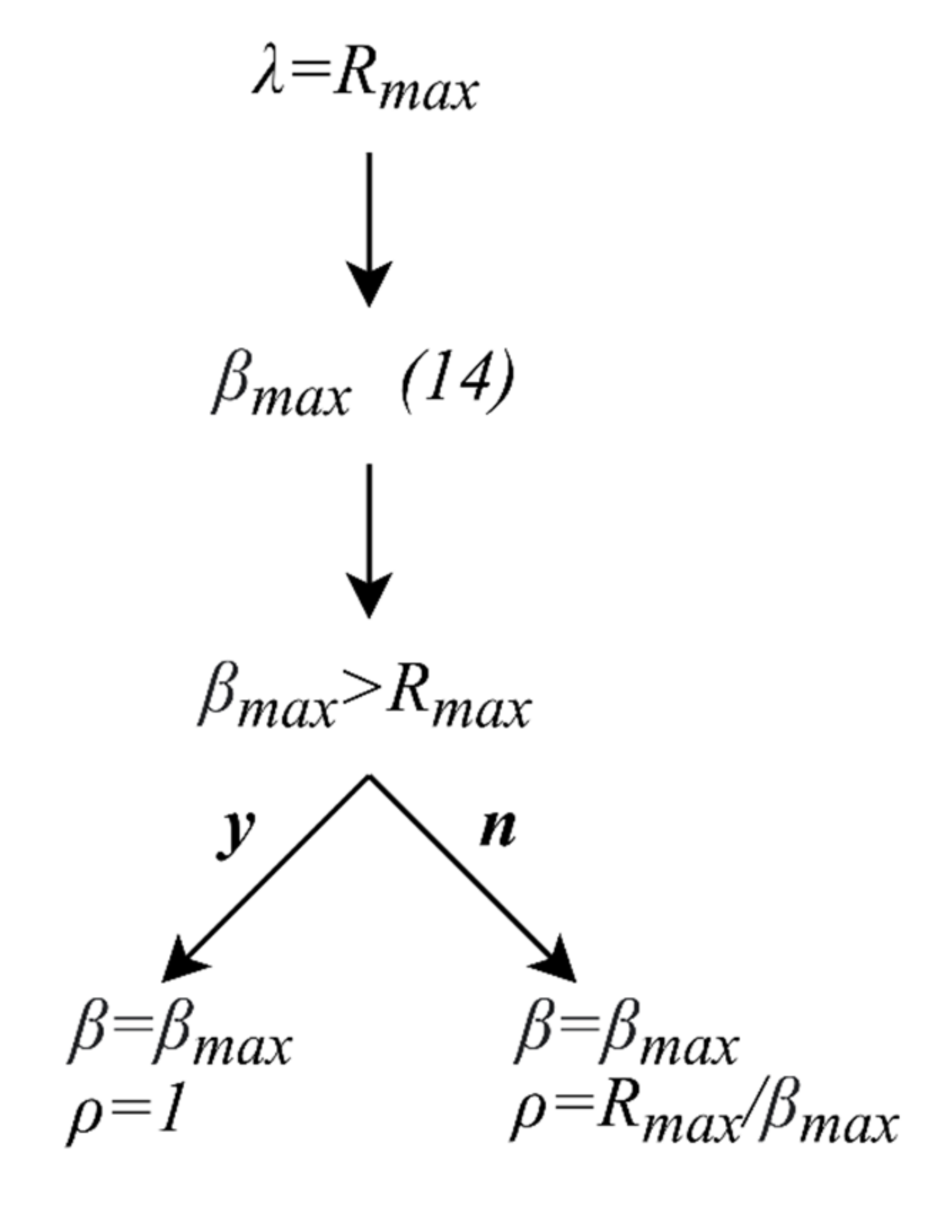
Figure 4.
Model for the common-mode half circuit of the proposed CMFB loop considering the offset of the inverters.
Figure 4.
Model for the common-mode half circuit of the proposed CMFB loop considering the offset of the inverters.

Figure 5.
Relative error of the dc output common-mode voltage vs. temperature and supply voltage.
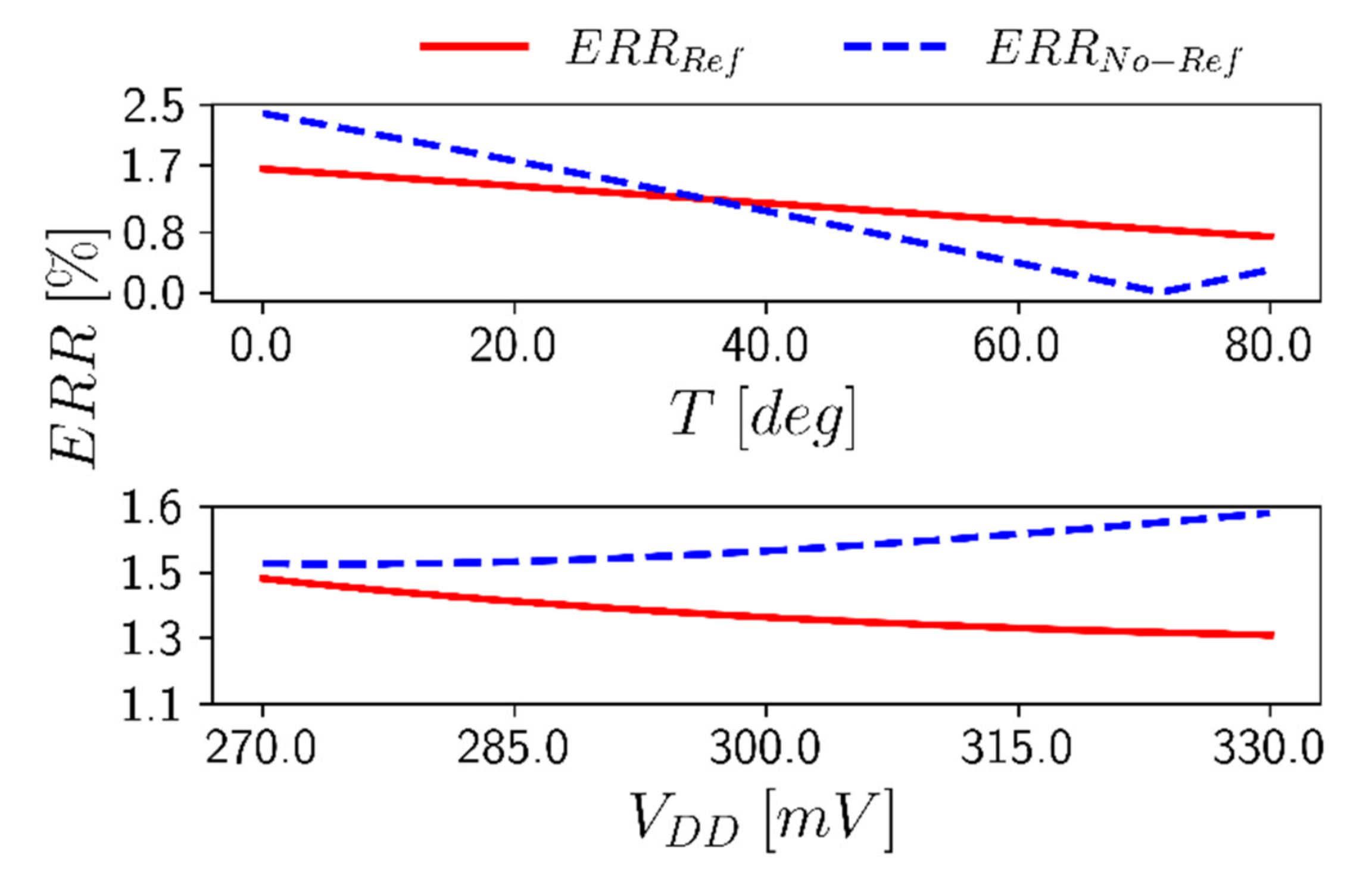
Figure 6.
Relative error (%) of the dc output common-mode voltage vs. process corners; darker colors correspond to higher relative errors.
Figure 6.
Relative error (%) of the dc output common-mode voltage vs. process corners; darker colors correspond to higher relative errors.
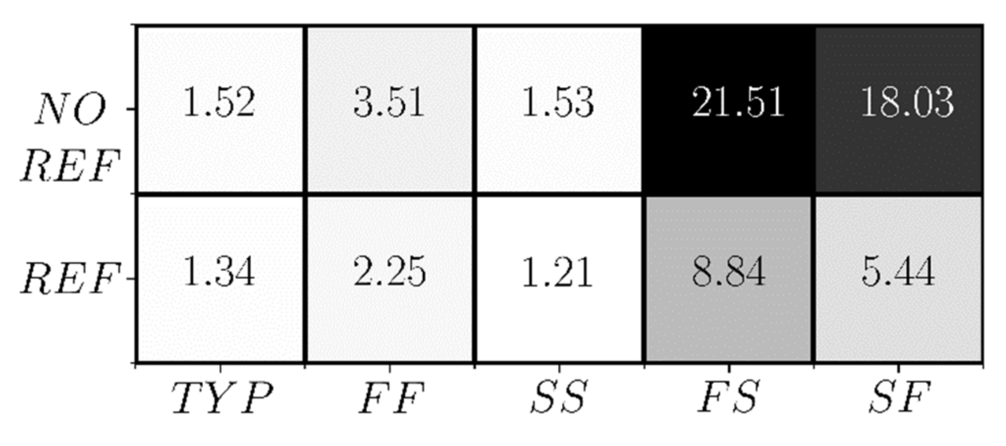
Figure 7.
Differential (red) and common-mode (blue) gain of the proposed OTA.
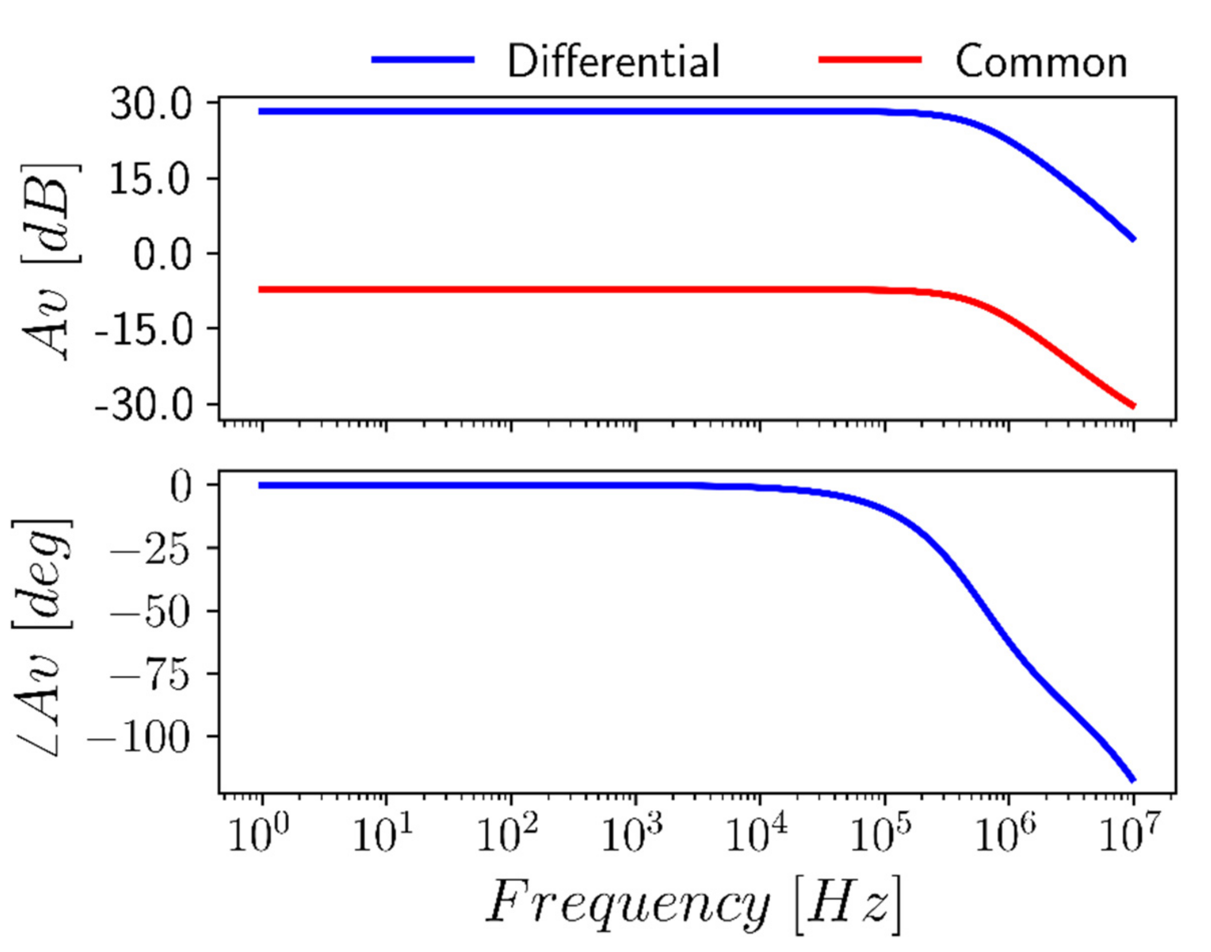
Figure 8.
Response of the OTA in unity-gain configuration to a 45-to-255 mV input step.

Figure 9.
Total Harmonic Distortion vs. input amplitude for a 1 MHz sinusoidal input signal.

Figure 10.
Input-referred noise spectrum of the OTA.

Figure 11.
Histogram of the CMRR for 200 Monte Carlo mismatch iterations.

Figure 12.
Layout of the proposed OTA generated by using the Cadence Innovus automatic place and route flow.
Figure 12.
Layout of the proposed OTA generated by using the Cadence Innovus automatic place and route flow.


Table 1.
Variations under process corners.
| Corner | FF | SS | FS | SF |
|---|---|---|---|---|
| AVD [dB] | 25.22 | 31.43 | 28.04 | 27.37 |
| GBW [MHz] | 26.4 | 10.24 | 15.28 | 14.57 |
| mφ [°] | 63.38 | 49.18 | 60.59 | 60.28 |
| Pd [μW] | 7.832 | 1.89 | 3.97 | 3.74 |
| VOS [mV] | 0.45 | 0.18 | 0.93 | 0.45 |
| SR [V/μs] | 15.15 | 5.85 | 12.47 | 6.33 |
Table 2.
Variations under supply voltage and temperature.
| Voltage Variations | Temperature Variations | |||
|---|---|---|---|---|
| T [°C] | 27 | 27 | 0 | 80 |
| VDD [mV] | 270 | 330 | 300 | 300 |
| AVD [dB] | 27.28 | 29.03 | 29.25 | 26.32 |
| GBW [MHz] | 10.03 | 23.03 | 9.80 | 29.41 |
| mφ [°] | 59.94 | 52.04 | 52.10 | 58.50 |
| Pd [μW] | 2.65 | 7.15 | 2.38 | 11.21 |
| VOS [mV] | −0.29 | −0.29 | −0.29 | 0.17 |
| SR [V/μs] | 3.61 | 12.52 | 6.91 | 12.88 |
Table 3.
Results of Monte Carlo mismatch analysis.
| Mean | Std | |
|---|---|---|
| AVD [dB] | 28.2 | 0.88 |
| GBW [MHz] | 15.78 | 1.91 |
| mϕ [°] | 54.47 | 3.12 |
| CMRR [dB] | 24.68 | 8.56 |
| Pd [μW] | 4.49 | 0.11 |
| VOS [mV] | 0.002 | 9.2 |
| SR [V/μs] | 9.12 | 1.02 |
Table 4.
Comparison with the literature.
| Ref | This Work | [30] | [31] | [17] | [18] | [46] | [10] | [12] | [35] | [36] | [3] |
|---|---|---|---|---|---|---|---|---|---|---|---|
| Year | 2022 | 2021 | 2021 | 2022 | 2022 | 2020 | 2020 | 2020 | 2019 | 2019 | 2015 |
| Tech. [nm] | 130 | 180 | 180 | 130 | 130 | 180 | 65 | 180 | 130 | 130 | 65 |
| VDD [V] | 0.3 | 0.55 | 0.3 | 0.3 | 0.3 | 0.3 | 0.25 | 0.5 | 0.3 | 0.25 | 0.35 |
| AVD [dB] | 28.3 | 87 | 30 | 38.1 | 52.9 | 39 | 70 | 79.5 | 49.8 | 25 | 43 |
| GBW [kHz] | 15,420 | 3150 | 0.25 | 24.14 | 35.16 | 0.9 | 9.5 | 36 | 9100 | 7.23 | 3600 |
| mφ [°] | 54 | 65 | 90 | 60 | 52 | 90 | 89 | 65 | 76 | 90 | 56 |
| CL [pF] | 1.5 | 250 | 150 | 50 | 50 | 10 | 15 | 15 | 2 | 30 | 3 |
| SRAVG [V/ms] | 9075 | 2.7 | 0.085 | 14.23 | 15.06 | -- | 2 | 9.7 | 3800 | -- | 5600 |
| Pd [nW] | 4406 | 8200 | 2.4 | 59.9 | 21.9 | 0.6 | 26 | 60 | 1800 | 55 | 17,000 |
| Area [μm2] | 164 | 88.3 | 982 | 2700 | 5200 | 472 | 2000 | 3395 | -- | 52,000 | 5000 |
| Type | STD | STD | DIG | BD | BD | IB | BD | BD | IB | IB | BD |
| FOMS [MHz pF/μW] | 5.25 | 96.04 | 15.62 | 20.15 | 80.31 | 15 | 5.48 | 9 | 10.11 | 3.94 | 0.63 |
| FOML [V pF/μs μW] | 3.09 | 0.08 | 5.31 | 11.88 | 34.40 | -- | 1.15 | 2.42 | 4.22 | -- | 0.99 |
| FOMS,A [MHz pF/μW μm2] | 32.01 | 1088 | 15.9 | 7.46 | 15.44 | 31.78 | 2.74 | 2.65 | -- | 0.07 | 0.13 |
| FOML,A [V pF/ms μW μm2] | 18.84 | 0.93 | 5.4 | 4.4 | 6.61 | -- | 0.57 | 0.71 | -- | -- | 0.19 |
STD = standard-cell-based; DIG s= DIGOTA; BD = body-driven; IB = inverter-based.
Publisher’s Note: MDPI stays neutral with regard to jurisdictional claims in published maps and institutional affiliations. |
© 2022 by the authors. Licensee MDPI, Basel, Switzerland. This article is an open access article distributed under the terms and conditions of the Creative Commons Attribution (CC BY) license (https://creativecommons.org/licenses/by/4.0/).
Share and Cite
MDPI and ACS Style
Centurelli, F.; Della Sala, R.; Scotti, G. A Standard-Cell-Based CMFB for Fully Synthesizable OTAs. J. Low Power Electron. Appl. 2022, 12, 27. https://doi.org/10.3390/jlpea12020027
AMA Style
Centurelli F, Della Sala R, Scotti G. A Standard-Cell-Based CMFB for Fully Synthesizable OTAs. Journal of Low Power Electronics and Applications. 2022; 12(2):27. https://doi.org/10.3390/jlpea12020027
Chicago/Turabian StyleCenturelli, Francesco, Riccardo Della Sala, and Giuseppe Scotti. 2022. "A Standard-Cell-Based CMFB for Fully Synthesizable OTAs" Journal of Low Power Electronics and Applications 12, no. 2: 27. https://doi.org/10.3390/jlpea12020027
Note that from the first issue of 2016, this journal uses article numbers instead of page numbers. See further details here.