Author Contributions
Conceptualization, C.G.-M. and M.C.S.; methodology, C.G.-M., M.C.S., C.M.A. and D.G.A.N.; software, C.M.A. and D.G.A.N.; validation, C.M.A. and D.G.A.N.; writing—original draft preparation, C.M.A. and D.G.A.N.; writing—review and editing, C.G.-M. and M.C.S.; visualization, C.M.A. and D.G.A.N.; supervision, C.G.-M.; funding acquisition, C.G.-M. and M.C.S. All authors have read and agreed to the published version of the manuscript.
Figure 1.
Symbol of an n-channel MOSFET transistor and its four terminals: gate (G), source (S), drain (D) and bulk (B). Source-drain symmetry illustrated by using currents.
Figure 1.
Symbol of an n-channel MOSFET transistor and its four terminals: gate (G), source (S), drain (D) and bulk (B). Source-drain symmetry illustrated by using currents.
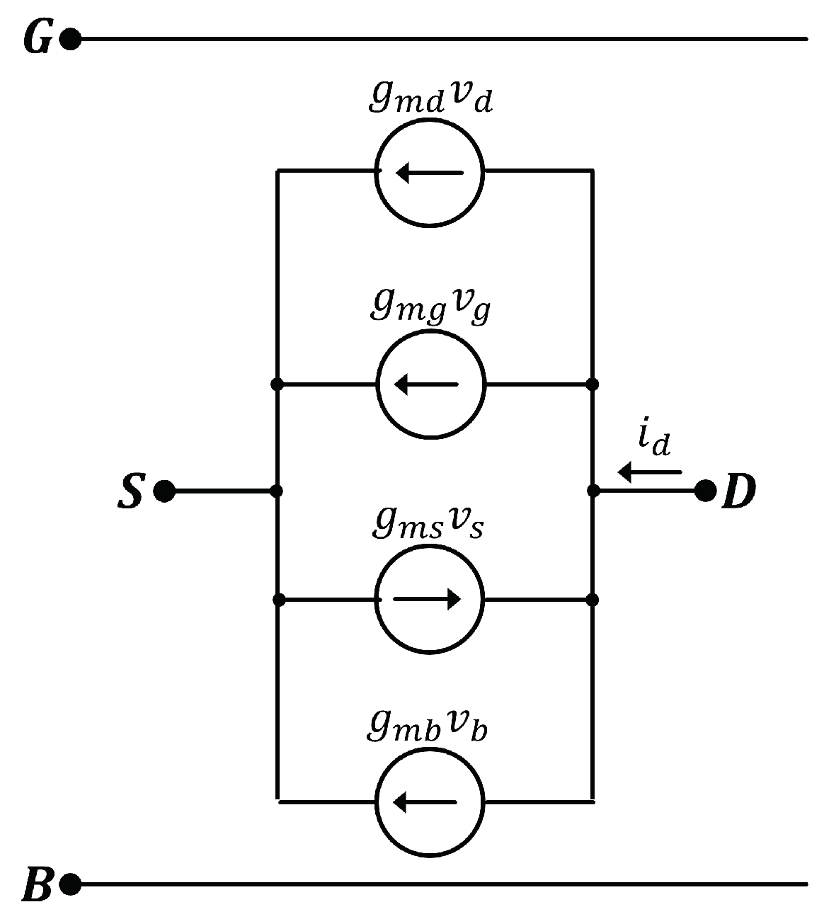
Figure 2.
Low-frequency small-signal model of the MOSFET.
Figure 2.
Low-frequency small-signal model of the MOSFET.
Figure 3.
MOSFET dynamic model with (
a) extrinsic and (
b) intrinsic parts [
13].
Figure 3.
MOSFET dynamic model with (
a) extrinsic and (
b) intrinsic parts [
13].
Figure 4.
Capacitances (
15)–(
19) normalized to
versus the pinch-off voltage for
.
Figure 4.
Capacitances (
15)–(
19) normalized to
versus the pinch-off voltage for
.
Figure 5.
(a) Circuit to extract parameters from (b) the and curves.
Figure 5.
(a) Circuit to extract parameters from (b) the and curves.
Figure 6.
(a) Circuit to determine the CSIG and (b) its equivalent small-signal model.
Figure 6.
(a) Circuit to determine the CSIG and (b) its equivalent small-signal model.
Figure 7.
Parameters of the 4PM vs. temperature of a medium (nominal) NMOS transistor with .
Figure 7.
Parameters of the 4PM vs. temperature of a medium (nominal) NMOS transistor with .
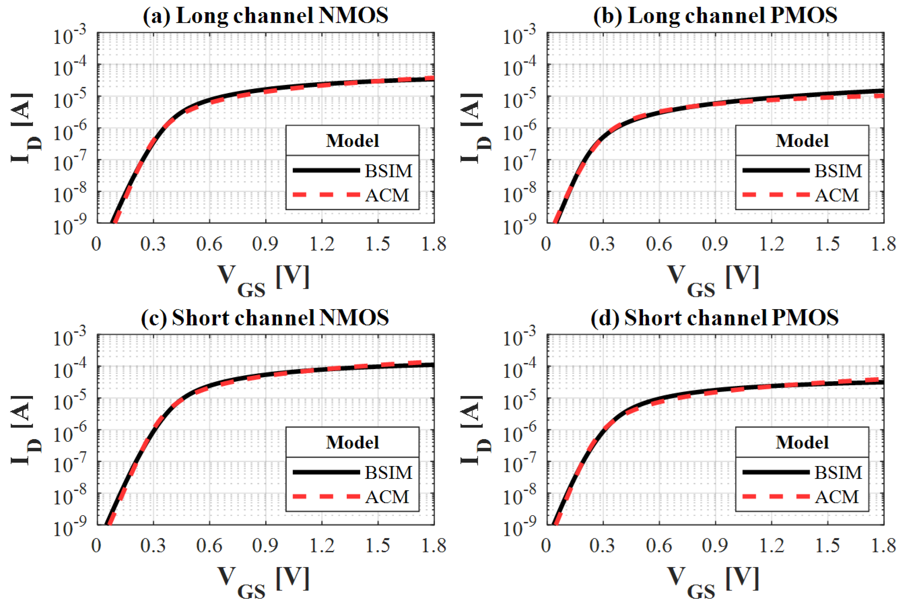
Figure 8.
mV for (a) medium (nominal) long-channel NMOS and (b) PMOS transistors and for (c) medium (nominal) short-channel NMOS and (d) PMOS transistors.
Figure 8.
mV for (a) medium (nominal) long-channel NMOS and (b) PMOS transistors and for (c) medium (nominal) short-channel NMOS and (d) PMOS transistors.
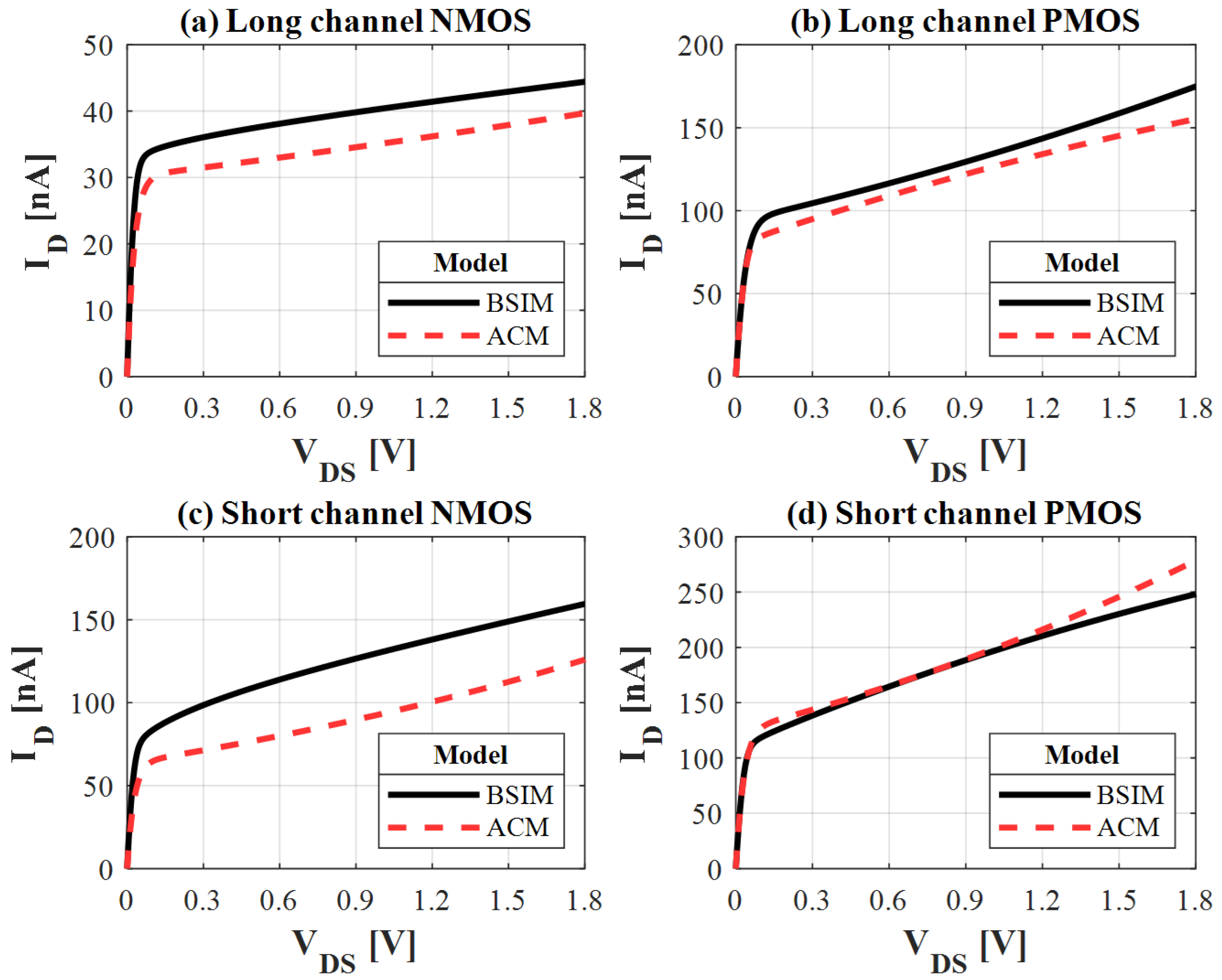
Figure 9.
mV for (a) medium (nominal) long-channel NMOS and (b) PMOS transistors and for (c) medium (nominal) short-channel NMOS and (d) PMOS transistors.
Figure 9.
mV for (a) medium (nominal) long-channel NMOS and (b) PMOS transistors and for (c) medium (nominal) short-channel NMOS and (d) PMOS transistors.
Figure 10.
The classic CMOS inverter.
Figure 10.
The classic CMOS inverter.
Figure 11.
CMOS inverter results of (a) voltage-transfer characteristic (VTC), (b) small-signal gain and (c) short-circuit current.
Figure 11.
CMOS inverter results of (a) voltage-transfer characteristic (VTC), (b) small-signal gain and (c) short-circuit current.
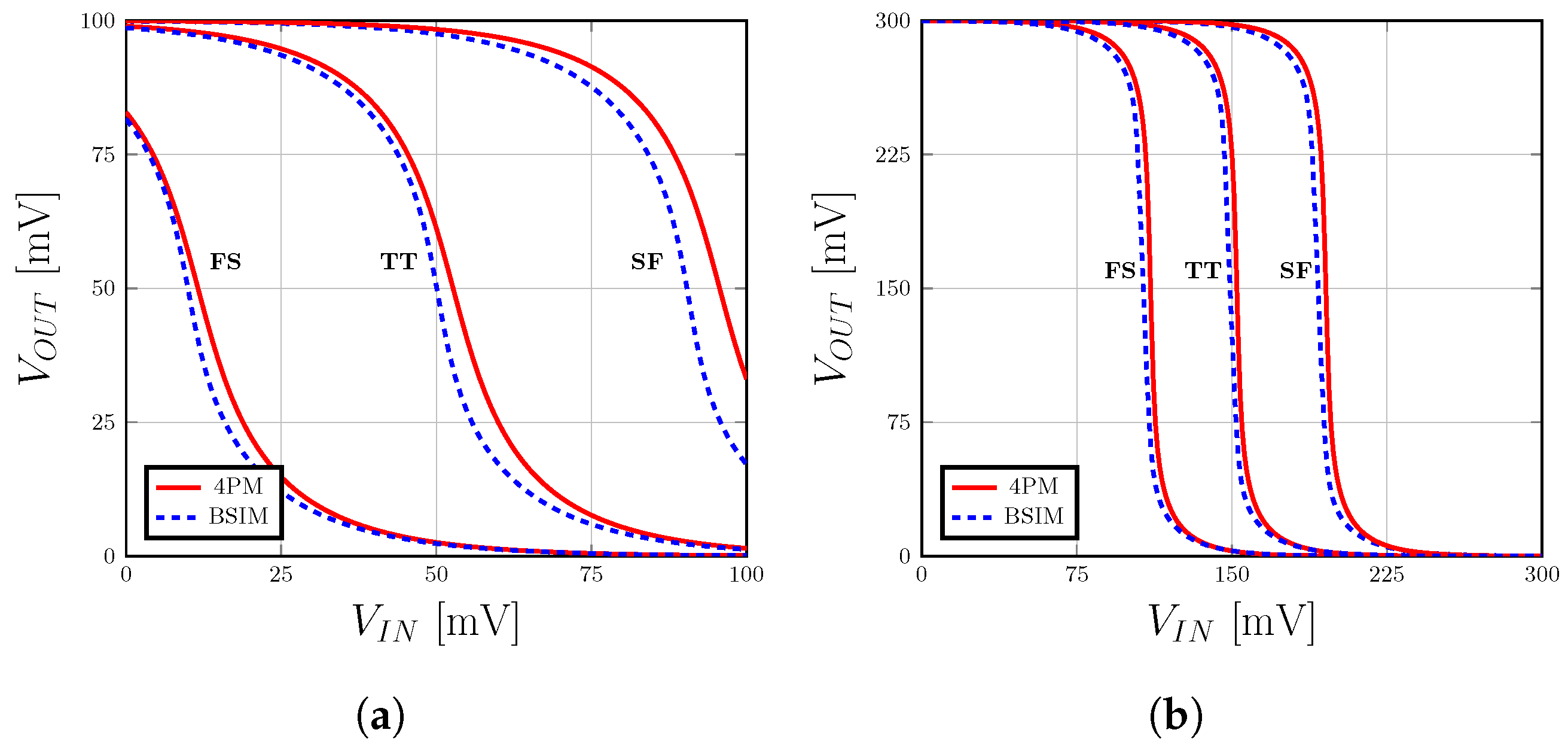
Figure 12.
Voltage-transfer characteristics of the CMOS inverter using BSIM and the 4PM across the corners of process variation. (a) = 100 mV. (b) = 300 mV.
Figure 12.
Voltage-transfer characteristics of the CMOS inverter using BSIM and the 4PM across the corners of process variation. (a) = 100 mV. (b) = 300 mV.
Figure 13.
Ring oscillator.
Figure 13.
Ring oscillator.
Figure 14.
Voltage signal in the time domain at one of the stages of the oscillator. Results for BSIM and 4PM simulations at 100 mV of supply voltage.
Figure 14.
Voltage signal in the time domain at one of the stages of the oscillator. Results for BSIM and 4PM simulations at 100 mV of supply voltage.
Figure 15.
Oscillation frequency vs. the supply voltage .
Figure 15.
Oscillation frequency vs. the supply voltage .
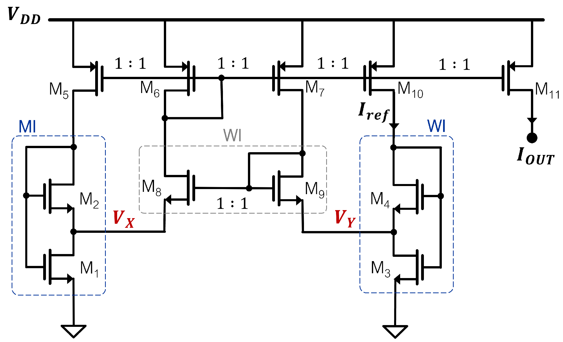
Figure 16.
Self-biased current source (SBCS) circuit.
Figure 16.
Self-biased current source (SBCS) circuit.
Figure 17.
Results of DC analysis for voltage sweep on : (a) output current, (b) and (c) .
Figure 17.
Results of DC analysis for voltage sweep on : (a) output current, (b) and (c) .
Figure 18.
Common-source amplifier.
Figure 18.
Common-source amplifier.
Figure 19.
Frequency response of the common-source amplifier using BSIM and 4PM: (a) open-loop gain in dB and (b) phase.
Figure 19.
Frequency response of the common-source amplifier using BSIM and 4PM: (a) open-loop gain in dB and (b) phase.
Table 1.
Extracted parameters for medium- NMOS/PMOS transistors with = .
Table 1.
Extracted parameters for medium- NMOS/PMOS transistors with = .
| Transistor | Slow | Nominal | Fast |
|---|
| NMOS | PMOS | NMOS | PMOS | NMOS | PMOS |
|---|
| [mV] | 316 | −239 | 291 | −211 | 266 | −183 |
| [nA] | 99 | 35 | 111 | 40 | 124 | 45 |
| n | 1.19 | 1.18 | 1.20 | 1.18 | 1.22 | 1.17 |
| 5.9 | 18 | 5.9 | 18 | 5.9 | 19 |
Table 2.
Extracted parameters for medium- NMOS/PMOS transistors with = .
Table 2.
Extracted parameters for medium- NMOS/PMOS transistors with = .
| Transistor | Slow | Nominal | Fast |
|---|
| NMOS | PMOS | NMOS | PMOS | NMOS | PMOS |
|---|
| [mV] | 338 | −272 | 311 | −239 | 283 | −206 |
| [nA] | 313 | 81 | 420 | 106 | 543 | 137 |
| n | 1.24 | 1.17 | 1.23 | 1.18 | 1.22 | 1.17 |
| 14 | 19 | 14 | 20 | 14 | 20 |
Table 3.
Corner-extracted parameters for medium- NMOS/PMOS transistors with = .
Table 3.
Corner-extracted parameters for medium- NMOS/PMOS transistors with = .
| Transistor | Slow | Nominal | Fast |
|---|
| NMOS | PMOS | NMOS | PMOS | NMOS | PMOS |
|---|
| [mV] | 339 | −308 | 309 | −269 | 280 | −230 |
| [nA] | 206 | 70 | 280 | 89 | 366 | 111 |
| n | 1.25 | 1.25 | 1.24 | 1.25 | 1.23 | 1.24 |
| 15 | 22 | 15 | 23 | 15 | 23 |
Table 4.
Oscillation frequency at various s obtained through time-domain simulations of the 11-stage ring oscillator without external .
Table 4.
Oscillation frequency at various s obtained through time-domain simulations of the 11-stage ring oscillator without external .
| BSIM | 4PM | |
|---|
| 400 mV | 81.3 MHz | 187.2 MHz | 2.30 |
| 300 mV | 23.7 MHz | 52.1 MHz | 2.20 |
| 200 mV | 3.79 MHz | 5.87 MHz | 1.55 |
| 100 mV | 452 kHz | 463 kHz | 1.02 |
| 60 mV | 198 kHz | 177 kHz | 0.89 |
Table 5.
Oscillation frequency at various s obtained through time-domain simulations of the 11-stage ring oscillator with external .
Table 5.
Oscillation frequency at various s obtained through time-domain simulations of the 11-stage ring oscillator with external .
| BSIM | 4PM | |
|---|
| 400 mV | 329.4 kHz | 316.2 kHz | 0.96 |
| 300 mV | 91.0 kHz | 94.4 kHz | 1.04 |
| 200 mV | 14.1 kHz | 12.3 kHz | 0.87 |
| 100 mV | 1.67 kHz | 1.12 kHz | 0.67 |
| 60 mV | 753 Hz | 469 Hz | 0.62 |
Table 6.
Sizes and and inversion levels of the transistors of the SBCS.
Table 6.
Sizes and and inversion levels of the transistors of the SBCS.
| Transistor | | |
|---|
| × | 15 |
| × | 0.32 |
| × | 0.01 |
| × | 0.1 |
| × | 10 |
Table 7.
Extracted parameters of transistors used in the SBCS.
Table 7.
Extracted parameters of transistors used in the SBCS.
| Transistor | NMOS | PMOS |
|---|
| W [m] | 0.5 | 4.0 | 0.5 |
| L [m] | 2.0 | 2.0 | 2.0 |
| [nA] | 29 | 63 | 10 |
| [mV] | 423 | 444 | −428 |
| n | 1.27 | 1.27 | 1.31 |
| [mV/V] | 2.2 | 2.4 | 6.5 |
Table 8.
Transistor dimensions for the common-source amplifier and extracted parameters.
Table 8.
Transistor dimensions for the common-source amplifier and extracted parameters.
| Transistor | | |
|---|
| W [m] | 2.0 | 0.5 |
|
L [m] | 0.18 | 2.0 |
| [nA] | 2000 | 10 |
| [mV] | 518 | −428 |
| n | 1.36 | 1.31 |
| [mV/V] | 21.8 | 6.5 |


 ,
, 


