
High-Speed and Energy-Efficient Carry Look-Ahead Adder


1
School of Computer Science and Engineering, Nanyang Technological University, 50 Nanyang Avenue, Singapore 639798, Singapore
2
Department of Industrial Engineering, Technical University of Sofia, 1000 Sofia, Bulgaria
*
Author to whom correspondence should be addressed.
J. Low Power Electron. Appl. 2022, 12(3), 46; https://doi.org/10.3390/jlpea12030046
Submission received: 2 June 2022
/
Revised: 19 July 2022
/
Accepted: 9 August 2022
/
Published: 10 August 2022
Abstract
:The carry look-ahead adder (CLA) is well known among the family of high-speed adders. However, a conventional CLA is not faster than other high-speed adders such as a conditional sum adder (CSA), a carry-select adder (CSLA), and the Kogge–Stone adder (KSA), which is the fastest parallel-prefix adder. Further, in terms of power-delay product (PDP) that characterizes the energy of digital circuits, the conventional CLA is not efficient compared to CSLA and KSA. In this context, this paper presents a high-speed and energy-efficient architecture for the CLA. Many adders ranging from ripple carry to parallel-prefix adders were implemented using a 32-28 nm CMOS standard digital cell library by considering a 32-bit addition. The adders were structurally described in Verilog and synthesized using Synopsys Design Compiler. From the results obtained, it is observed that the proposed CLA achieves a reduction in critical path delay by 55.3% and a reduction in PDP by 45% compared to the conventional CLA. Compared to the CSA, the proposed CLA achieves a reduction in critical path delay by 33.9%, a reduction in power by 26.1%, and a reduction in PDP by 51.1%. Compared to an optimized CSLA, the proposed CLA achieves a reduction in power by 35.4%, a reduction in area by 37.3%, and a reduction in PDP by 37.1% without sacrificing the speed. Although the KSA is faster, the proposed CLA achieves a reduction in power by 39.6%, a reduction in PDP by 6.5%, and a reduction in area by 55.6% in comparison.
1. Introduction
Addition is a fundamental operation that is pervasive in computer arithmetic [1]. For example, approximately 80% of the operations in an ARM processor’s arithmetic and logic unit were found to be additions [2]. Addition is physically realized using an adder, and the design of a high-speed and low power/energy-efficient adder is important for processing units. There are different types of adders ranging from the slowest ripple carry adder (RCA) to the fastest Kogge–Stone adder (KSA) [3], which is a parallel-prefix adder (PPA). However, it may be noted that although the KSA is faster, the RCA is area- and power-efficient in comparison. Based on physical realization using a 32-28 nm CMOS standard digital cell library [4], for a 32-bit addition, we noted that the KSA has a 78.5% reduced delay than the RCA while the RCA requires 86% less silicon area and dissipates 50.4% less power in comparison. The RCA and the KSA represent the two extremes in physically realizing addition where the former requires the least area and dissipates less power but is slower while the latter is of high-speed but requires more area and dissipates relatively more power. Nevertheless, there are many high-speed adders such as the carry look-ahead adder (CLA), the conditional sum adder (CSA), the carry-select adder (CSLA), and other PPAs that offer a trade-off between the standard design metrics, namely speed, power, and area. These high-speed adders lie between the extreme addition architectures, i.e., RCA and KSA. Hence, for a practical application, and particularly from a standard cell-based design perspective, the choice of an adder would be dependent upon the power budget and/or operational speed.
Besides speed (whose reciprocal is called delay i.e., critical path delay) and power, the product of power and delay, which is called the power-delay product (PDP), is representative of the energy consumption of digital circuits [5]. PDP is considered to be a low-power and low-energy figure of merit. Since power and delay are preferred to be less for a digital circuit, therefore, PDP is preferred to be less. Hence, an adder that offers a good trade-off between speed, power, and energy (PDP) is preferable for generic applications. In this context, this paper presents a CLA architecture that is higher in speed and energy-efficient compared to a conventional CLA architecture. Additionally, this paper provides a comparison between the performance of different adders, which would be useful for a circuit designer to make an appropriate choice of an adder for a target application by considering the trade-offs in the design metrics.
CLA is an important member of the family of high-speed adders [6]. Many implementations of the CLA at the transistor level have been presented in the literature [7,8,9,10,11,12,13,14], which correspond to different design styles such as the all N-type transistor logic, static CMOS, BiCMOS, domino logic, etc. Further, CLAs designed using post-CMOS technologies such as quantum dot cellular automata, memristors, hybrid CMOS-memristor logic, optical, carbon nanotube, vertically stacked nanowire transistors, etc. [15,16,17,18,19,20,21], have also been presented in the literature. All these represent full-custom design approaches that require considerable manual effort to meet timing/power/energy requirements commensurate with an application. On the other hand, a semi-custom gate-level design would be generic and modular and a soft CLA core can be offered as a synthesizable RTL model that can be conveniently used/reused in any digital system design and can be implemented using any standard digital cell library. In this context, this paper presents a generic gate-level CLA architecture that is higher in speed and energy-efficient compared to the conventional gate-level CLA architecture.
The rest of the paper is organized into three sections. Section 2 discusses the architectures of the conventional CLA and the proposed CLA. Section 3 presents the design metrics of several 32-bit adders corresponding to different architectures, which were implemented using a 32-28 nm CMOS standard digital cell library and compares their performance. Section 4 gives the conclusion.
2. Conventional and Proposed CLA Architectures
In an adder implementation, the sum bit corresponding to an input bit position is produced based on a knowledge of any carry input and the carry may be generated and/or propagated internally between the input bit positions. Hence, considering the worst-case addition scenario where the carry may propagate internally from the 0th bit position up to the (N–1)th bit position of an N-bit adder, speeding up the carry propagation internally would help to speed up the addition process. The linear time encountered in a rudimentary worst-case addition (which is the case with an RCA) can be reduced to a logarithmic time addition in the case of a CLA by generating future (look-ahead) carries in advance based on a knowledge of the carry input. The generalized carry look-ahead equation is given in (1), where Q represents a bit position, CQ represents the carry input to the Qth bit position, CQ+1 represents the carry output from the Qth bit position, GQ refers to the generate signal, and PQ refers to the propagate signal corresponding to the Qth bit position. In Equation (1), PQ is obtained by performing a logical XOR of input bits XQ and YQ (i.e., PQ = XQ ⊕ YQ), and GQ is obtained by performing a logical AND of input bits XQ and YQ (i.e., GQ = AQBQ). The sum bit corresponding to the Qth bit position is produced based on Equation (2).
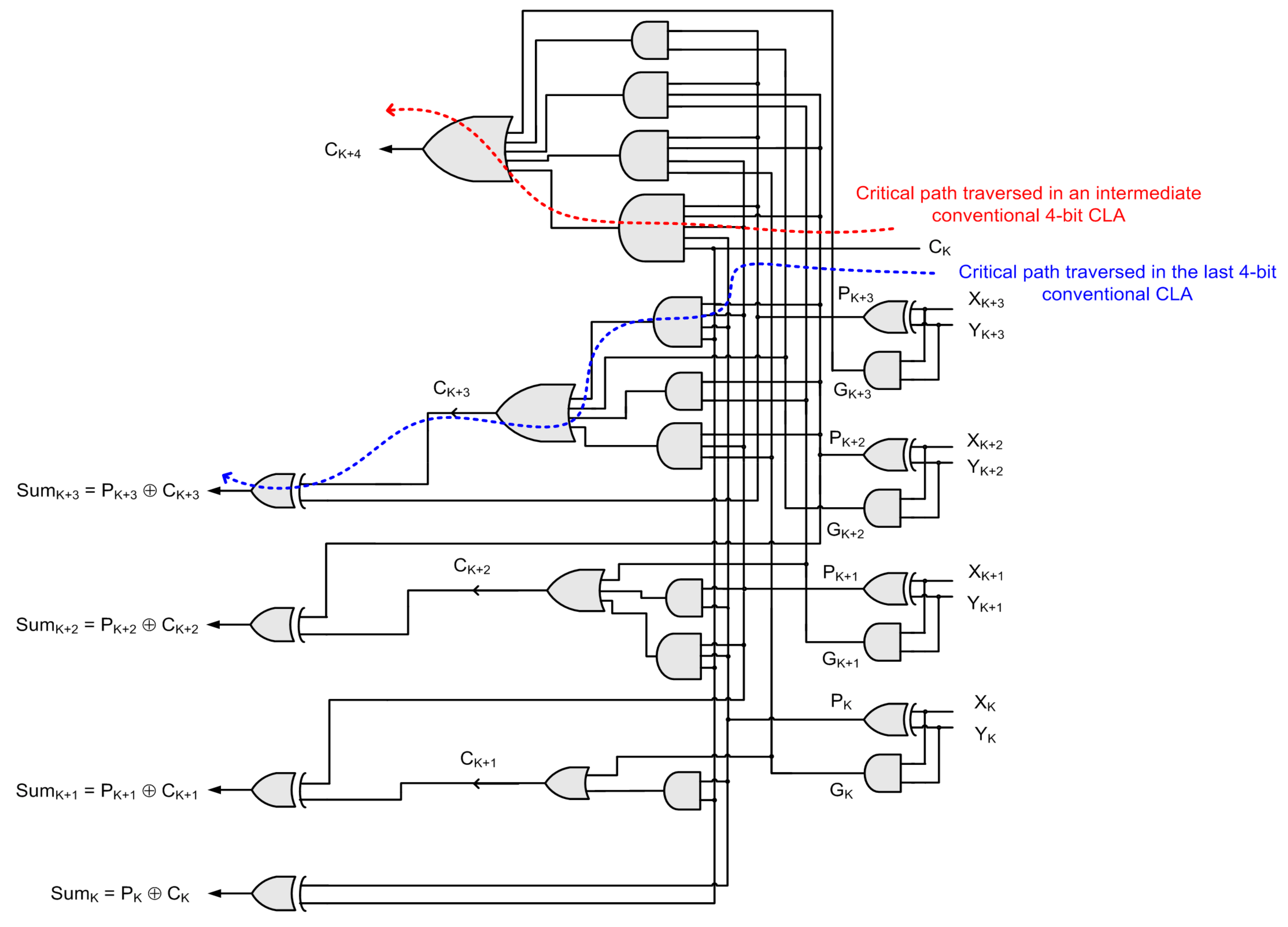
Equation (1) is fundamentally recursive in nature, and this property can be utilized to generate carries corresponding to successive bit positions in advance, which are called look-ahead carries. This is described by Equations (3)–(6), which represent the look-ahead carry output equations of four successive bit positions of an example 4-bit CLA. In Equations (3)–(6), CK represents the carry input to a 4-bit CLA, PK+3 to PK represent the propagate signals, GK+3 to GK represent the generate signals, and CK+4 to CK+1 represent the look-ahead carry outputs derived. Equation (4) is deduced by substituting the expression of CK+1 given in Equation (3), Equation (5) is deduced by substituting the expression of CK+2 given in Equation (4), and Equation (6) is deduced by substituting the expression of CK+3 given in Equation (5). In Equations (3)–(6), it can be observed that the look-ahead carry outputs CK+1 up to CK+4 are all dependent on only the carry input CK. Hence, the look-ahead carry outputs can be generated in parallel, which can be used to generate the sum bits of the CLA in parallel and provide the carry input to the subsequent stage. The conventional CLA implementing Equations (3)–(6) is shown in Figure 1.
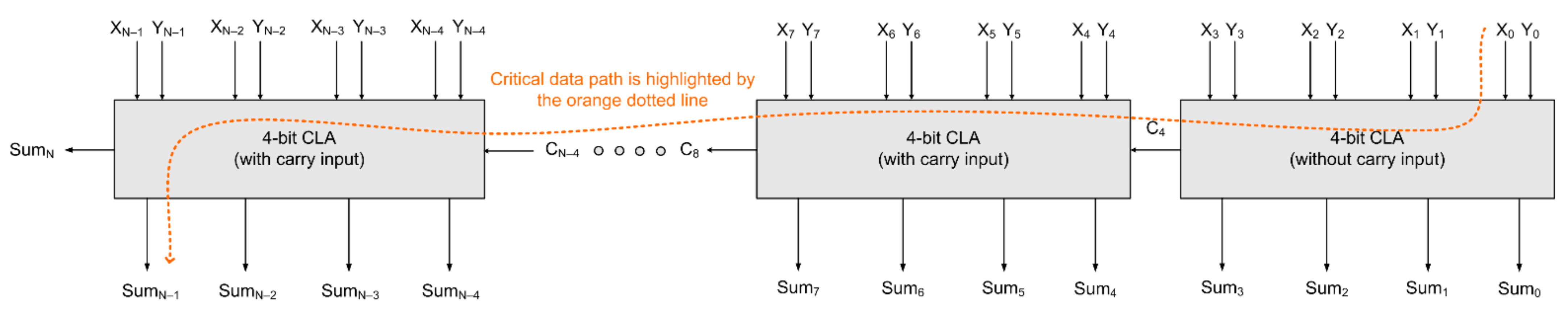
Typically, an N-bit CLA is constructed using a cascade of M-bit CLAs where N and M are even and N modulo M = 0. For example, a 32-bit CLA can be constructed by cascading eight 4-bit CLAs. Figure 2 shows a block diagram of an N-bit CLA constructed using 4-bit CLAs, and the critical path is highlighted by the orange dotted line. Supposing that the 4-bit CLA shown in Figure 1 is present in an intermediate stage of an N-bit CLA, as shown in Figure 2, then theoretically the critical path that would be traversed through the 4-bit CLA would be as highlighted by the red dashed line in Figure 1, which consists of a 5-input AND gate and a 5-input OR gate. In modern standard digital cell libraries, the fan-in of AND and OR gates are limited to four. So, a 5-input AND/OR gate may be decomposed into a combination of two 3-input AND/OR gates, respectively. Supposing the 4-bit CLA shown in Figure 1 is present in the last stage of Figure 2, then the critical path that would be traversed is highlighted by the blue dashed line shown in Figure 1.
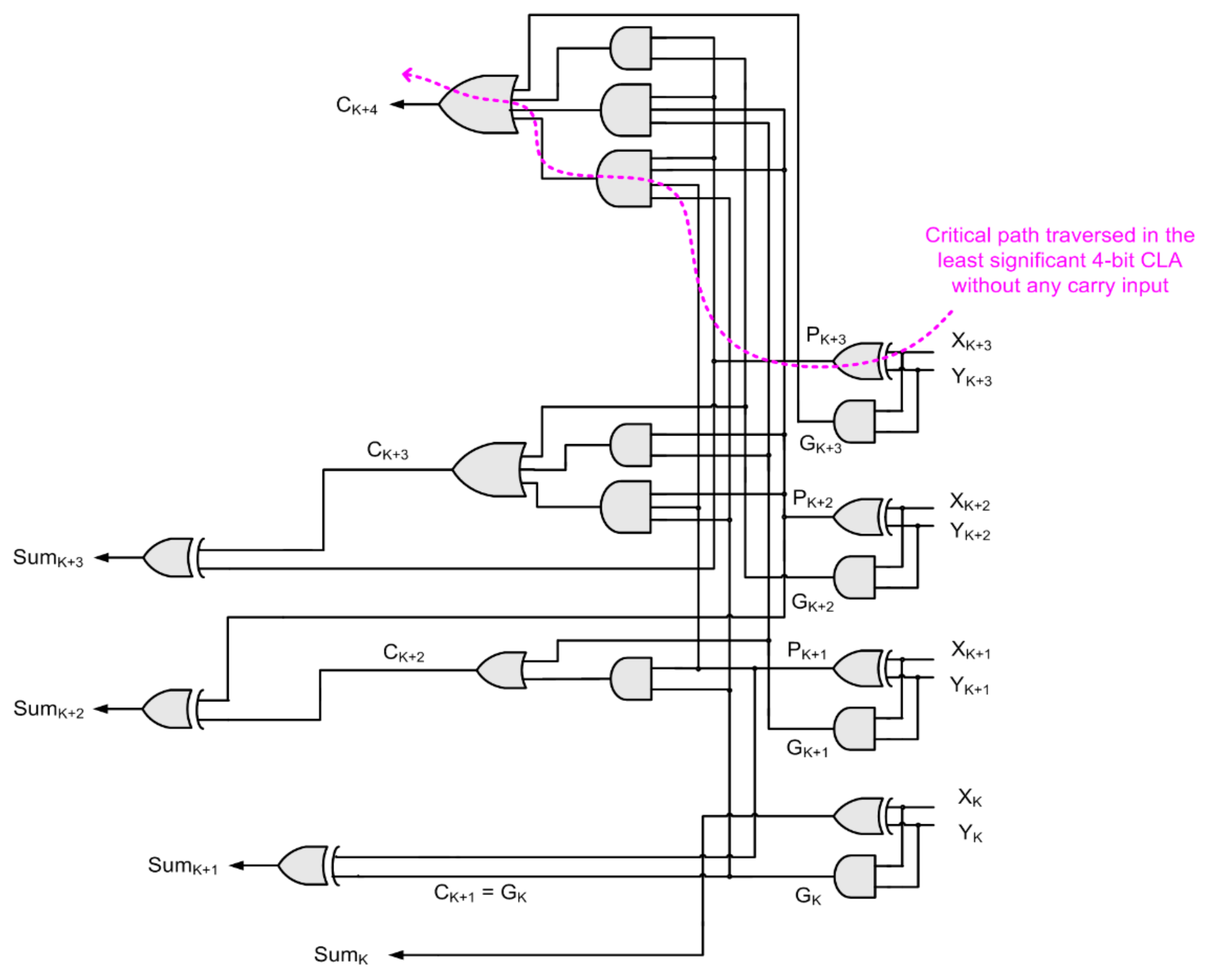
In Figure 2, it can be seen that the first (least significant) 4-bit CLA does not have a carry input while the rest of the 4-bit CLAs have a carry input. Hence, in the absence of a carry input, i.e., considering CK = 0 in Equations (3)–(6), the gate-level realization of a 4-bit CLA without any carry input would be as shown in Figure 3, and its critical path is highlighted by the pink dashed line.
Referring to Figure 1, Figure 2 and Figure 3, the theoretical critical path delay of a conventional N-bit CLA, which includes only gate delays, is expressed by Equation (7). In Equation (7), on the right-side, the first term given within brackets represents the propagation delay encountered in producing the penultimate sum bit SumN–1, the second term given within brackets represents the propagation delay encountered in traversing (M–2) 4-bit CLAs, and the last term represents the propagation delay encountered in traversing the least significant 4-bit CLA that does not have a carry input. The second term on the right-side of Equation (7) reflects the optimum decomposition of 5-input OR and 5-input AND gates seen in Figure 1 into two 3-input OR gates and two 3-input AND gates, respectively.
Assuming that a 32-bit CLA has been constructed using eight conventional 4-bit CLAs (i.e., M = 8), and using the average propagation delay information of gates with minimum drive strength given in [4], the theoretical critical path delay () of the conventional 32-bit CLA is calculated to be 2.106 ns.
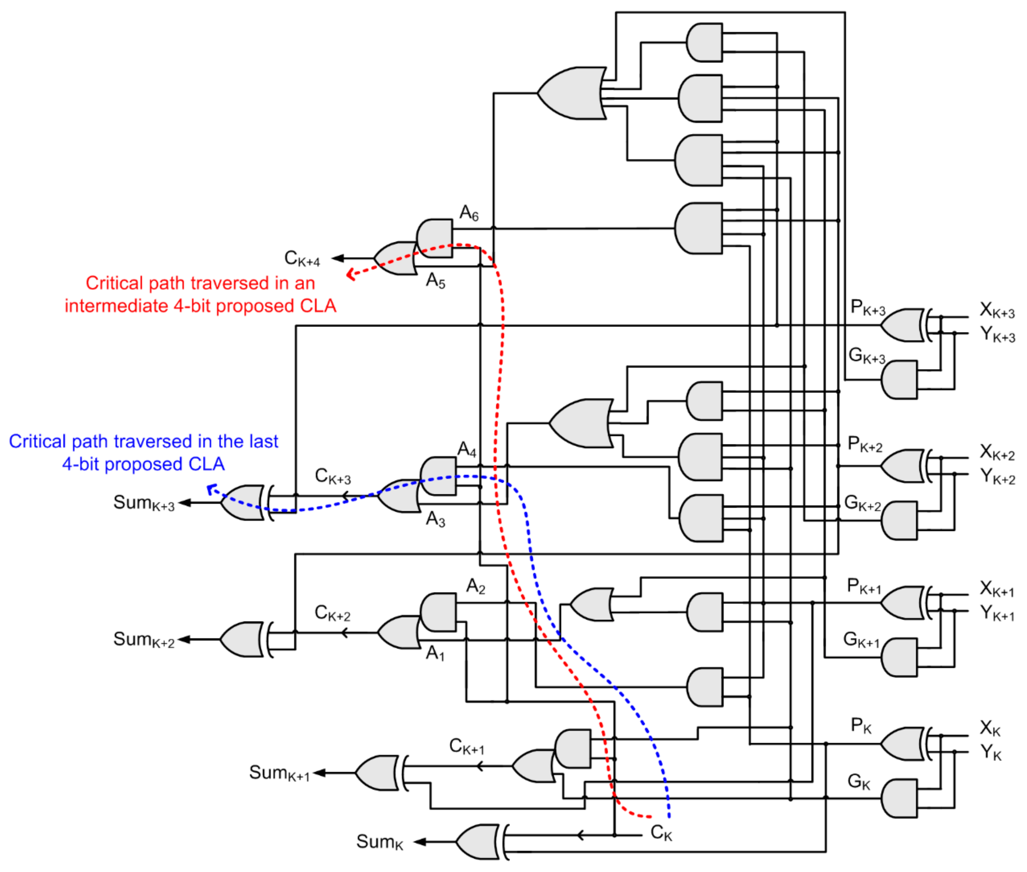
For the new CLA design, we performed a specific grouping of the terms present in the look-ahead carry output equations such that the carry propagation would be minimized with respect to a gate-level realization. The general principle followed is that the literals associated with the carry input (CK) are grouped into an intermediate product term and represented using a Boolean variable, and the remaining sum of product terms that do not involve the carry input are grouped and represented using another Boolean variable. With reference to Equations (4)–(6), to perform the grouping, we introduced some intermediate variables in the Boolean network, namely A1, A2, A3, A4, A5, and A6, where A1 and A2 are used for Equation (4), A3 and A4 are used for Equation (5), and A5 and A6 are used for Equation (6), and they are expressed by Equations (8)–(13) given below. In fact, this grouping procedure is generic and can be applied to a CLA of any size by incorporating only two intermediate variables in each look-ahead carry output equation. Supposing only two intermediate variables are present in a look-ahead carry output equation, as is the case with Equation (3), it can be retained as such, and no transformation needs to be done. In general, a CLA featuring L look-ahead carry outputs may require (2L–2) intermediate variables according to our proposition.
Given Equations (8)–(13), and substituting them back into Equations (4)–(6), we obtain their reduced forms as follows.
Consequently, the final logic level of the look-ahead carry outputs CK+1, CK+2, CK+3, and CK+4 can be uniformly realized using a single complex gate, viz., the AO21 gate. Assuming that A, B, and C are the inputs to an AO21 gate and Y is its output, an AO21 gate implements the logic function Y = AB + C, which requires eight transistors for a static CMOS logic design.
The logic realization of an example proposed 4-bit CLA, described by Equations (3) and (14)–(16), is portrayed by Figure 4. The critical path that would be traversed when this 4-bit CLA would be present in an intermediate stage in Figure 2 is highlighted by the red dashed line and the critical path that would be traversed when this 4-bit CLA would be present in the final stage in Figure 2 is highlighted by the blue dashed line.
Comparing Figure 1 and Figure 4, it can be noted that the critical path of a conventional 4-bit CLA, when present in an intermediate stage, consists of a 5-input AND gate and a 5-input OR gate while the critical path of the proposed 4-bit CLA, when present in an intermediate stage, consists of just one AO21 complex gate. As a result, the theoretical critical path delay of the proposed N-bit CLA (shown in Figure 2), when implemented using the proposed 4-bit CLA, is given by Equation (17). However, for the least significant 4-bit CLA that does not contain a carry input, Figure 3 can be used as mentioned earlier.
Assuming that a 32-bit CLA has been constructed using eight proposed 4-bit CLAs (i.e., M = 8), and using the average propagation delay information of gates with the minimum drive strength given in [4], the theoretical critical path delay () of the proposed 32-bit CLA is calculated to be 0.781 ns, which is 63% less than the theoretical critical path delay of the conventional CLA counterpart given by (7).
3. Implementation and Estimation of Design Metrics of Adders
In the existing literature, many papers dealt with specific adder designs, discussed their implementation, and presented the design metrics, but failed to provide a comparison with the design metrics of other adder architectures. For example, [22] presented a new CSLA design and made a comparison between the design metrics of just the conventional CSLA and the new CSLA. Reference [23] provided a comparison between CLA and CSLA architectures but the adders were custom-designed at the gate-level and interconnects were not taken into account in the estimation of design metrics—hence the design metric estimates provided are not rigorous. Here, we aim to provide a rigorous and extensive comparison between the performance of various adders corresponding to different architectures, including the proposed CLA, with all the adders realized using the same standard digital cell library. This comparative evaluation would be useful for a circuit designer to choose an appropriate adder when given specific design constraints. Towards this, we described many 32-bit adders corresponding to different architectures, viz., RCA, CLA, CSLA, CSA, and PPA structurally at the gate-level in Verilog HDL. We used Synopsys EDA tools for synthesis, simulation, and estimation of the design metrics. We had access to some Synopsys DesignWare library components that contain synthesizable RTL models of some high-speed adders such as the Ling adder [24] (which is a variant of CLA), CSA [25], and a few PPAs, namely the Brent–Kung adder (BKA) [26] and the Sklansky adder [27]. We considered all these adders for implementation and comparison in this paper. Besides, we considered the RCA, the conventional CLA, the proposed CLA, CSLAs without a binary to excess-one code (BEC) converter [28] employing two different input partitions, viz., 8-8-8-8 and 8-7-6-4-3-2-2, CSLAs with a BEC converter employing the same two input partitions [22], and the KSA. We used the gate-level description of a 32-bit KSA given in [29] for implementation in this work.
To perform synthesis, we used the Synopsys Design Compiler and targeted a typical case PVT specification of a high Vth 32-28 nm CMOS standard digital cell library. The recommended supply voltage of 1.05V and an operating junction temperature of 25 °C was used. A default wire load model was included during synthesis and a fanout-of-4 drive strength was associated with all the output ports (i.e., sum bits) of the adders. The high-speed adder components present in the DesignWare library, i.e., the Ling adder, CSA, BKA, and Sklansky adder, were invoked during synthesis and these were synthesized along with the rest of the high-speed adders mentioned earlier by using the ‘compile’ command with speed defined as the optimization goal. To synthesize the RCA, the ‘compile_ultra’ command was used. After synthesis, the gate-level netlists generated by Design Compiler were used to perform a functional simulation using Synopsys VCS. To do this, a test bench comprising approximately 1000 randomly generated input vectors was supplied to the adders at an input frequency of 250 MHz and their functionality were verified and their corresponding switching activity were recorded. The switching activity information was then used to accurately estimate the total average power using Synopsys PrimePower. To accurately estimate the critical path delay of adders, we used Synopsys PrimeTime. The total area of the adders estimated after synthesis, including the cells area and interconnect area, was estimated using Design Compiler. The design metrics of the adders are given in Table 1.
From Table 1, it is seen that the RCA requires the least area and hence it dissipates less power. This is because the RCA is synthesized using 1 half adder and 31 full adders, and the full adder and half adder are available as cells in the standard digital cell library [4], which are optimized for area and power. However, the critical path delay of the RCA is significantly greater compared to its counterparts, which makes it unsuitable for high-speed digital circuits and systems. For example, compared to the proposed CLA, the RCA has a 200% greater delay. As expected, in terms of speed, the KSA is faster than its counterparts—however, this comes at the expense of a substantially greater area and power dissipation. For example, compared to the proposed CLA, the KSA has a 35.3% reduced delay but requires a 125.3% greater area and dissipates 65.6% more power. The conventional CLA dissipates less power than the proposed CLA by 18.8% since it requires 26.4% less area but reports an approximate 124% increase in the delay. In terms of delay, the rest of the adders lie in between the two adders, viz., the RCA and the KSA with the former having the greatest delay and the latter having the least delay.
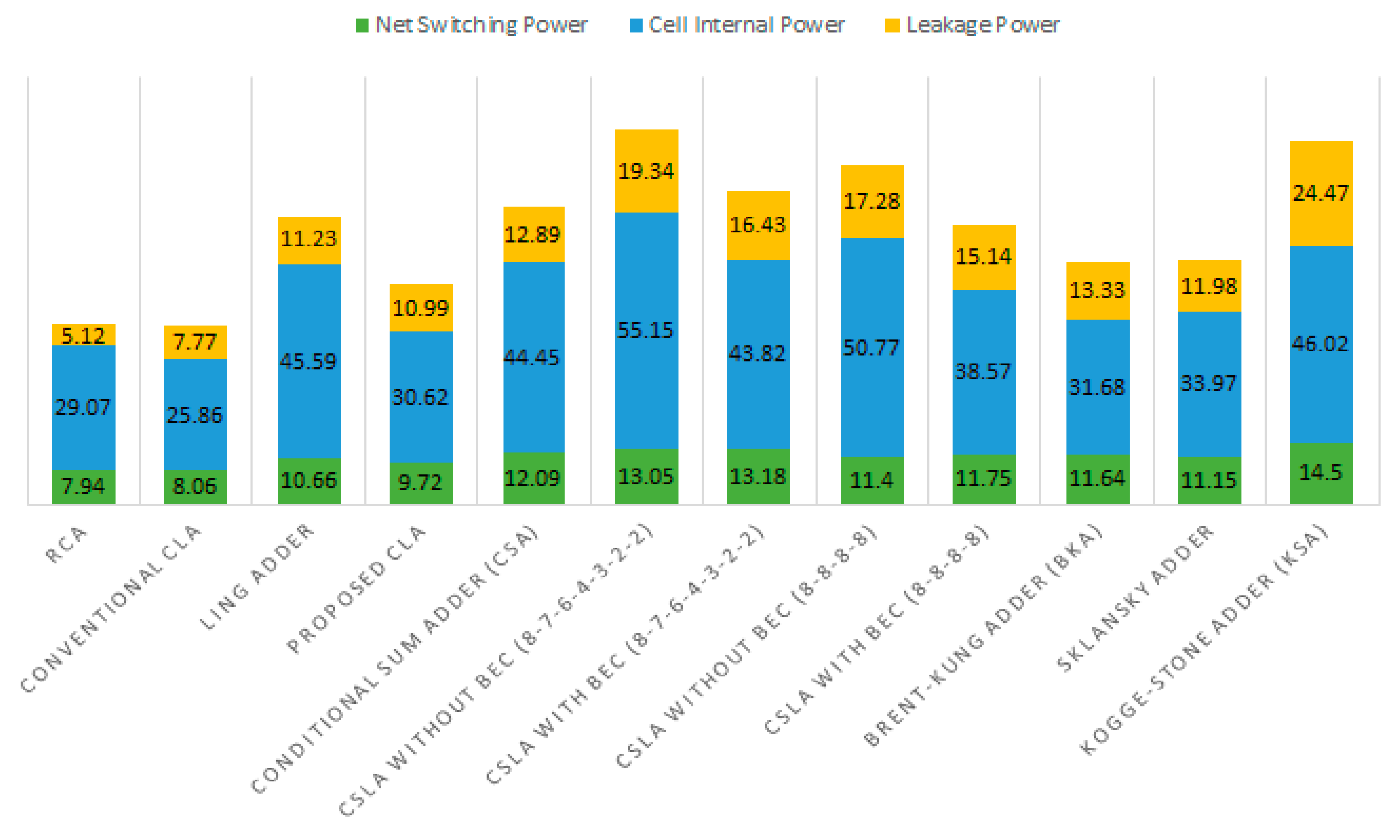
Figure 5 shows a split-up of the power components of different adders that includes the net switching power, the cell internal power, and the leakage power, as reported by Synopsys PrimePower. The sum of the net switching power and the cell internal power is referred to as dynamic power in Synopsys PrimePower. The total power is the sum of the dynamic power and leakage power. It may be seen that the proposed CLA reports increases in all the power components compared to the conventional CLA. This is mainly because the cells area and interconnect area of the proposed CLA are greater than the conventional CLA, as seen from Table 1. Compared to the RCA and the conventional CLA, the proposed CLA reports an increase in total power due to an increase in all the power components, but the proposed CLA dissipates less total power compared to the other adders due to reductions achieved in the switching power, internal power, and leakage power, as seen from Figure 5. Although the KSA is faster than its counterparts, as seen from Table 1, it dissipates substantially more power and this is due to its greater area occupancy both in terms of cells and interconnect, which is reflected by its significant values of net switching power, cell internal power and leakage power in Figure 5.
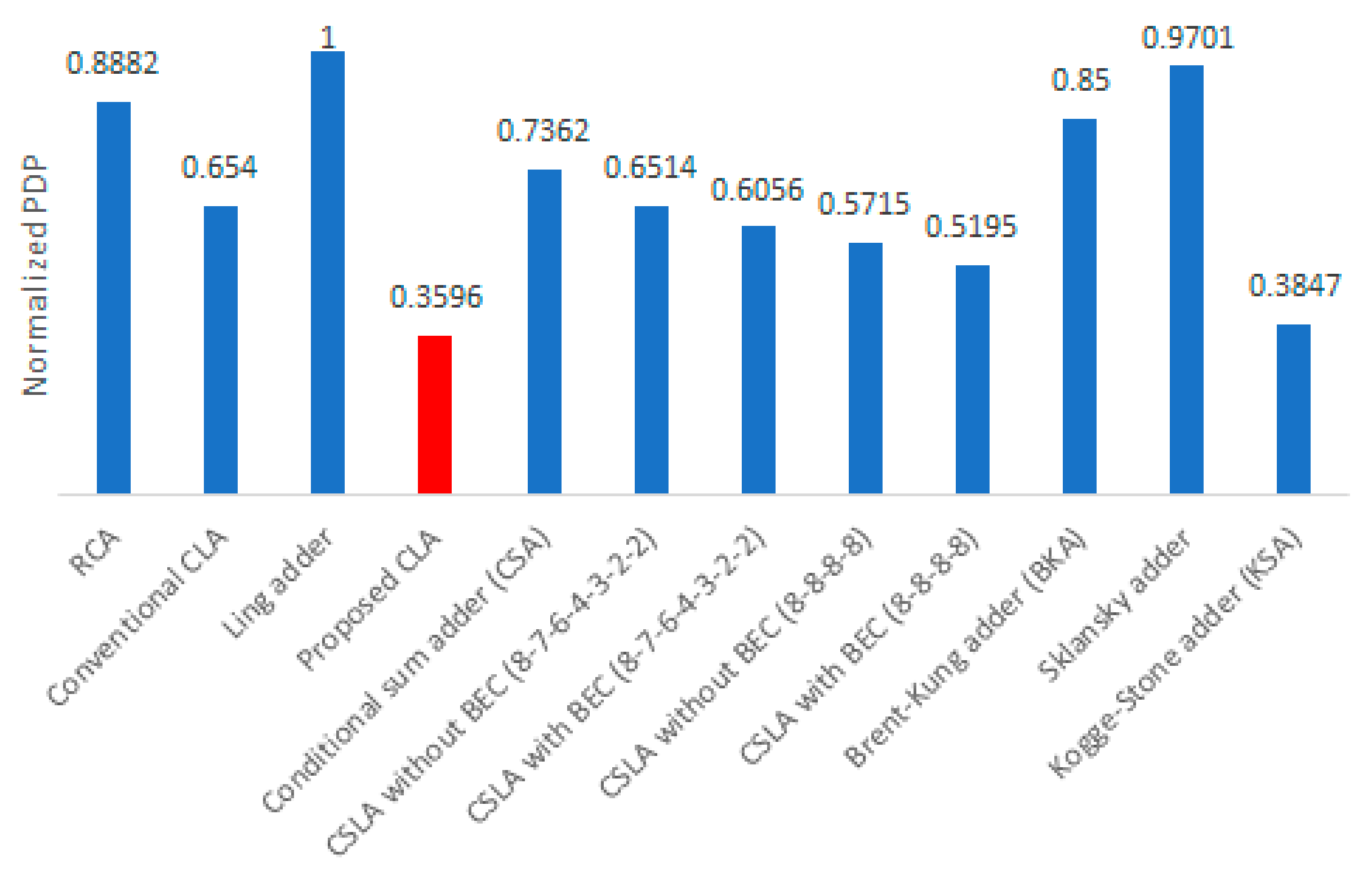
Besides the individual considerations of delay and power, it is important to analyze the performance of adders from an energy perspective, which is given by the product of total power and the critical path delay. This is because an evaluation of energy gives information about any trade-off between power and delay in a digital circuit [5]. Since power and delay are preferred to be less, therefore, the product of power and delay (PDP) is preferred to be less. In other words, the lesser the PDP, the more energy-efficient is a design. PDP was calculated for all the adders and those values were then normalized. To perform the normalization, the highest PDP value (corresponding to the Ling adder) was used to divide the actual PDP of all the adders. The normalized PDP plots of the adders are shown in Figure 6 with the optimum plot shown in red. An adder with a lesser normalized PDP value is preferable. Given this, the Ling adder is found to be less energy-efficient compared to the other adders. From Figure 6, it is seen that the proposed CLA has an optimized normalized PDP compared to its counterparts, which implies the proposed CLA is more energy-efficient. Compared to the conventional CLA, the proposed CLA is 45% more energy-efficient. The KSA consumes 7% more energy than the proposed CLA, although it is faster, and this is due to its increased power dissipation in comparison on account of its greater area occupancy. Hence, from Table 1 and Figure 6, it may be concluded that the proposed CLA offers a good trade-off between speed, power, and area compared to its counterparts.
4. Conclusions
CLA is a popular member of the family of high-speed adders. However, the conventional CLA architecture is not faster than some high-speed adders and this is mainly due to the greater delay encountered in the carry propagation. In this context, this paper presented an improved architecture for the CLA that significantly reduces the delay in the carry propagation. The theoretical and practical delay estimates confirm the significant reduction in delay achieved by the proposed CLA compared to the conventional CLA. For a 32-bit addition, the proposed CLA achieves a 55.3% reduction in delay compared to the conventional CLA and is 45% more energy-efficient.
Author Contributions
Conceptualization, P.B.; methodology, P.B. and N.E.M.; formal analysis, P.B. and N.E.M.; validation, P.B.; visualization, P.B.; investigation, P.B.; data curation, P.B.; writing—original draft preparation, P.B. All authors have read and agreed to the published version of the manuscript.
Funding
This research received no external funding.
Institutional Review Board Statement
Not applicable.
Informed Consent Statement
Not applicable.
Data Availability Statement
All data are available within the manuscript.
Conflicts of Interest
The authors declare no conflict of interest.
References
- Hennessy, J.; Patterson, D. Computer Architecture: A Quantitative Approach, 5th ed.; Morgan Kaufmann: Burlington, MA, USA, 2003; ISBN 9780123838735. [Google Scholar]
- Garside, J.D. A CMOS VLSI implementation of an asynchronous ALU. In Proceedings of the IFIP Working Conference on Asynchronous Design Methodologies, Manchester, UK, 31 March–2 April 1993. [Google Scholar]
- Kogge, P.M.; Stone, H.S. A parallel algorithm for the efficient solution of a general class of recurrence equations. IEEE Trans. Comput. 1973, 100, 786–793. [Google Scholar] [CrossRef]
- Synopsys SAED_EDK32/28_CORE Databook. Revision 1.0.0. 2012. Available online: https://www.synopsys.com/community/university-program/teaching-resources.html (accessed on 8 December 2021).
- Rabaey, J.M.; Chandrakasan, A.; Nikolic, B. Digital Integrated Circuits: A Design Perspective, 2nd ed.; Pearson Education: London, UK, 2003; ISBN 978-0130909961. [Google Scholar]
- Parhami, B. Computer Arithmetic: Algorithms and Hardware Designs, 1st ed.; Oxford University Press: New York, NY, USA, 2000; ISBN 978-0195125832. [Google Scholar]
- Kuo, J.B.; Liao, H.J.; Chen, H.P. A BiCMOS dynamic carry lookahead adder circuit for VLSI implementation of high-speed arithmetic unit. IEEE J. Solid-State Circuits 1993, 28, 375–378. [Google Scholar] [CrossRef]
- Ruiz, G.A. New static multi-output carry lookahead CMOS adders. IEE Proc. Circuits Devices Syst. 1997, 144, 350–354. [Google Scholar] [CrossRef]
- Lim, J.; Kim, D.-G.; Chae, S.-I. A 16-bit carry-lookahead adder using reverse energy recovery logic for ultra-low-energy systems. IEEE J. Solid-State Circuits 1999, 34, 898–903. [Google Scholar]
- Wang, C.-C.; Huang, C.-J.; Tsai, K.-C. A 1.0-GHz, 0.6-µm 8-bit carry lookahead adder using PLA-styled all-N transistor logic. IEEE Trans. Circuits Syst. II Analog. Digit. Signal Processing 2000, 47, 133–135. [Google Scholar] [CrossRef]
- Yang, G.; Jung, S.O.; Baek, K.-H.; Kim, S.H.; Kim, S.; Kang, S.-M. A 32-bit carry lookahead adder using dual-path all-N logic. IEEE Trans. VLSI Syst. 2005, 13, 992–996. [Google Scholar] [CrossRef]
- Wang, C.-C.; Huang, C.-C.; Lee, C.-L.; Cheng, T.-W. A low power high-speed 8-bit pipelining CLA design using dual-threshold voltage domino logic. IEEE Trans. VLSI Syst. 2008, 16, 594–598. [Google Scholar] [CrossRef] [Green Version]
- Zlatanovici, R.; Kao, S.; Nikolic, B. Energy-delay optimization of 64-bit carry-lookahead adders with a 240 ps 90 nm CMOS design example. IEEE J. Solid-State Circuits 2009, 44, 569–583. [Google Scholar] [CrossRef]
- Morgenshtein, A.; Yuzhaninov, V.; Kovshilovsky, A.; Fish, A. Full-swing gate diffusion input logic—Case-study of low-power CLA adder design. Integr. VLSI J. 2014, 47, 62–70. [Google Scholar] [CrossRef]
- Cho, H.; Swartzlander, E.E. Adder designs and analyses for quantum-dot cellular automata. IEEE Trans. Nanotechnol. 2007, 6, 374–383. [Google Scholar] [CrossRef]
- Lopez, J.F.; Reina, R.; Hernandez, L.; Tobajas, F.; de Armas, V.; Sarmiento, R.; Nunez, A. Pipelined GaAs carry lookahead adder. Electron. Lett. 1998, 34, 1732–1733. [Google Scholar] [CrossRef]
- Shaltoot, A.H.; Madian, A.H. Memristor based carry lookahead adder architectures. In Proceedings of the IEEE 55th International Midwest Symposium on Circuits and Systems, Boise, ID, USA, 5–8 August 2012. [Google Scholar]
- Liu, G.; Zheng, L.; Wang, G.; Shen, Y.; Liang, Y. A carry lookahead adder based on hybrid CMOS-memristor logic circuit. IEEE Access 2019, 7, 43691–43696. [Google Scholar] [CrossRef]
- Dutta, P.; Bandyopadhyay, C.; Giri, C.; Rahaman, H. Mach-Zehnder interferometer based all optical reversible carry-lookahead adder. In Proceedings of the IEEE Computer Society Annual Symposium on VLSI, Tampa, FL, USA, 9–11 July 2014. [Google Scholar]
- Sun, Y.; Kursun, V. Low-power and compact NP dynamic CMOS adder with 16nm carbon nanotube transistors. In Proceedings of the IEEE International Symposium on Circuits and Systems, Beijing, China, 19–23 May 2013. [Google Scholar]
- Sacchetto, D.; Ben-Jamaa, M.H.; de Micheli, G.; Leblebici, Y. Design aspects of carry lookahead adders with vertically-stacked nanowire transistors. In Proceedings of the IEEE International Symposium on Circuits and Systems, Paris, France, 30 May–2 June 2010. [Google Scholar]
- Ramkumar, B.; Kittur, H.M. Low-power and area-efficient carry select adder. IEEE Trans. Very Large Scale Integr. Syst. 2012, 20, 371–375. [Google Scholar] [CrossRef]
- Balasubramanian, P.; Mastorakis, N. Performance comparison of carry-lookahead and carry-select adders based on accurate and approximate additions. Electronics 2018, 7, 369. [Google Scholar] [CrossRef] [Green Version]
- Ling, H. High-speed binary adder. IBM J. Res. Dev. 1981, 25, 156–166. [Google Scholar] [CrossRef]
- Sklansky, J. Conditional-sum addition logic. IRE Trans. Electron. Comput. 1960, EC-9, 226–231. [Google Scholar] [CrossRef]
- Brent, R.P.; Kung, H.T. A regular layout for parallel adders. IEEE Trans. Comput. 1982, C-31, 260–264. [Google Scholar] [CrossRef]
- Sklansky, J. An evaluation of several two-summand binary adders. IRE Trans. Electron. Comput. 1960, EC-9, 213–226. [Google Scholar] [CrossRef]
- Bedrij, O.J. Carry-select adder. IRE Trans. Electron. Comput. 1962, EC-11, 340–346. [Google Scholar] [CrossRef]
- Yazdanbakhsh, A.; Mahajan, D.; Esmaeilzadeh, H.; Lofti-Kamran, P. AxBench: A multiplatform benchmark suite for approximate computing. IEEE Des. Test 2017, 34, 60–68. [Google Scholar] [CrossRef]
Figure 1.
Gate-level realization of a conventional 4-bit CLA with carry input CK.

Figure 2.
Block diagram of an N-bit CLA realized using a cascade of 4-bit CLAs, where N is even.

Figure 3.
Gate-level realization of a 4-bit conventional CLA without carry input (i.e., CK = 0).

Figure 4.
Gate-level realization of 4-bit proposed CLA (with carry input).

Figure 5.
Split-up of total power dissipation of different adders, estimated using PrimePower.

Figure 6.
Normalized PDP of different 32-bit adders (lesser value is preferable, which is highlighted by the red bar). The PDP of Ling adder is considered to be the baseline as it is higher and the PDP of all the adders are divided by the baseline value to obtain the normalized PDP plots.
Figure 6.
Normalized PDP of different 32-bit adders (lesser value is preferable, which is highlighted by the red bar). The PDP of Ling adder is considered to be the baseline as it is higher and the PDP of all the adders are divided by the baseline value to obtain the normalized PDP plots.


Table 1.
Design metrics of 32-bit adders, synthesized using a 32-28 nm CMOS standard cell library.
| Adder Name | Area (µm2) | Critical Path Delay (ns) | Total Power (µW) | ||
|---|---|---|---|---|---|
| Cells | Interconnect | Total | |||
| RCA | 155.03 | 10.98 | 166.01 | 3.40 | 42.13 |
| Conventional CLA | 350.97 | 37.44 | 388.41 | 2.53 | 41.69 |
| Ling adder (CLA variant) | 392.40 | 75.21 | 467.61 | 2.39 | 67.48 |
| Proposed CLA | 475.50 | 51.94 | 527.44 | 1.13 | 51.33 |
| Conditional sum adder (CSA) | 412.48 | 77.65 | 490.13 | 1.71 | 69.43 |
| CSLA without BEC (8-7-6-4-3-2-2) | 834.35 | 117.82 | 952.17 | 1.20 | 87.54 |
| CSLA with BEC (8-7-6-4-3-2-2) | 683.65 | 96.22 | 779.87 | 1.33 | 73.43 |
| CSLA without BEC (8-8-8-8) | 745.15 | 95.86 | 841.01 | 1.16 | 79.45 |
| CSLA with BEC (8-8-8-8) | 621.89 | 81.90 | 703.79 | 1.28 | 65.46 |
| Brent–Kung adder (BKA) | 419.85 | 64.40 | 484.25 | 2.42 | 56.65 |
| Sklansky adder | 387.06 | 62.75 | 449.81 | 2.74 | 57.10 |
| Kogge–Stone adder (KSA) | 1014.29 | 174.43 | 1188.72 | 0.73 | 84.99 |
Publisher’s Note: MDPI stays neutral with regard to jurisdictional claims in published maps and institutional affiliations. |
© 2022 by the authors. Licensee MDPI, Basel, Switzerland. This article is an open access article distributed under the terms and conditions of the Creative Commons Attribution (CC BY) license (https://creativecommons.org/licenses/by/4.0/).
Share and Cite
MDPI and ACS Style
Balasubramanian, P.; Mastorakis, N.E. High-Speed and Energy-Efficient Carry Look-Ahead Adder. J. Low Power Electron. Appl. 2022, 12, 46. https://doi.org/10.3390/jlpea12030046
AMA Style
Balasubramanian P, Mastorakis NE. High-Speed and Energy-Efficient Carry Look-Ahead Adder. Journal of Low Power Electronics and Applications. 2022; 12(3):46. https://doi.org/10.3390/jlpea12030046
Chicago/Turabian StyleBalasubramanian, Padmanabhan, and Nikos E. Mastorakis. 2022. "High-Speed and Energy-Efficient Carry Look-Ahead Adder" Journal of Low Power Electronics and Applications 12, no. 3: 46. https://doi.org/10.3390/jlpea12030046
Note that from the first issue of 2016, this journal uses article numbers instead of page numbers. See further details here.