
Speed, Power and Area Optimized Monotonic Asynchronous Array Multipliers


1
School of Computer Science and Engineering, Nanyang Technological University, 50 Nanyang Avenue, Singapore 639798, Singapore
2
Department of Industrial Engineering, Technical University of Sofia, 1000 Sofia, Bulgaria
*
Author to whom correspondence should be addressed.
J. Low Power Electron. Appl. 2024, 14(1), 1; https://doi.org/10.3390/jlpea14010001
Submission received: 3 November 2023
/
Revised: 14 December 2023
/
Accepted: 20 December 2023
/
Published: 24 December 2023
Abstract
:Multiplication is a fundamental arithmetic operation in electronic processing units such as microprocessors and digital signal processors as it plays an important role in various computational tasks and applications. There exist many designs of synchronous multipliers in the literature. However, in the domain of Input–Output Mode (IOM) asynchronous design, there is relatively less published research on multipliers. Some existing works have considered quasi-delay-insensitive (QDI) asynchronous implementations of multipliers. However, the QDI asynchronous design paradigm, in general, is not area- and speed-efficient. This article presents an efficient alternative implementation of IOM asynchronous multipliers based on the concept of monotonic Boolean networks. The array multiplier architecture has been considered for demonstrating the usefulness of our proposition. The building blocks of the multiplier, such as the partial product generator, half adder, and full adder, were implemented monotonically. The popular dual-rail encoding scheme was considered for encoding the multiplier inputs and outputs, and four-phase return-to-zero handshaking (RZH) and return-to-one handshaking (ROH) were separately considered for communication. Compared to the best of the existing QDI asynchronous array multipliers, the proposed monotonic asynchronous array multiplier achieves the following reductions in design metrics: (i) a 40.1% (44.3%) reduction in cycle time (which is the asynchronous equivalent of synchronous clock timing), a 37.7% (37.7%) reduction in area, and a 4% (4.5%) reduction in power for 4 × 4 multiplication corresponding to RZH (ROH), and (ii) a 58.1% (60.2%) reduction in cycle time, a 45.2% (45.2%) reduction in area, and a 10.3% (11%) reduction in power for 8 × 8 multiplication corresponding to RZH (ROH). The multipliers were implemented using a 28 nm CMOS process technology.
1. Introduction
Computer arithmetic is ubiquitous in general-purpose and application-specific digital processing, and arithmetic circuits such as adders and multipliers etc. are predominantly present in the data path of a processing unit. Moreover, arithmetic operations tend to be responsible for most of the power consumption. For example, about 70% of the power consumed by a graphics processing unit is attributed to arithmetic operations [1], and about 80% of the power consumed by a fast Fourier transform processor is attributed to adders and multipliers [2]. Multiplication is a fundamental arithmetic operation in electronic processing units such as microprocessors and digital signal processors as it plays a crucial role in various computational tasks and applications. For example, digital signal processing algorithms, used in image and audio processing applications, frequently involve multiplication for tasks such as filtering, Fourier transforms, convolution, and modulation. Conventionally, multiplication is realized in a synchronous design style, and there are many synchronous multipliers reported in the literature. However, the Input–Output Mode (IOM) asynchronous design style is an appealing alternative to the synchronous design style, since IOM asynchronous circuits possess inherent modularity and resilience due to their insensitivity to delays [3,4]. Moreover, unlike synchronous circuits, IOM asynchronous circuits can adapt to variations in process, voltage, and temperature [5], exhibit reduced vulnerability to electromagnetic interference [6], offer enhanced security against attacks when compared to synchronous circuits [7], and self-checking [8].
In the domain of IOM asynchronous design, there is relatively less research work on multipliers. This may be because IOM asynchronous design is unorthodox and very different from conventional synchronous design [9]. Among the existing works, [10,11] presented some full-custom (transistor-level) designs based on the concept of null convention logic [12] while refs. [13,14,15] presented some semi-custom (gate-level) designs. Compared to full-custom designs, which require extensive manual characterization, semi-custom designs are preferable as they can use the available gates from a standard cell library, which are pre-characterized. However, the Muller C-element [16], which is widely used in an IOM asynchronous design, is not usually available in a commercial or open-source standard digital cell library, so that should be separately implemented and incorporated into an IOM asynchronous design. Compared to full-custom designs of the C-element [17,18], a semi-custom C-element design is rather convenient to implement by incorporating feedback into an AO222 complex gate, as shown in [19]. For this work, we considered the same static CMOS complex gate-based C-element design given in [19].
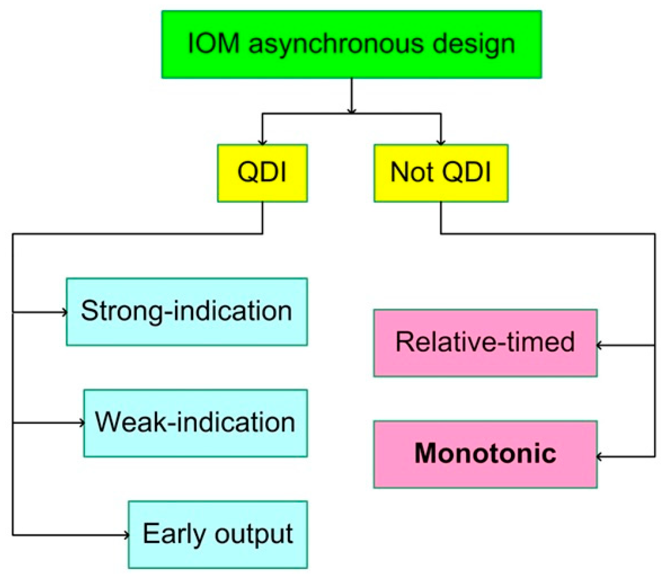
IOM asynchronous design, in general, is classified into two types viz. quasi-delay-insensitive (QDI) and non-QDI, as depicted in Figure 1. The QDI design style is typically more robust than the non-QDI design style, as it offers delay insensitivity internally and externally to a circuit and involves the full completion of internal processing before producing all the primary outputs, but is inferior in terms of the design metrics. The non-QDI design style may offer delay insensitivity only externally to a circuit and so it does not require the full completion of internal processing to produce all the primary outputs. This characteristic enables it to achieve significant reductions in design metrics compared to the QDI design style. Nevertheless, both these design styles generally encode the inputs and outputs and adopt a four-phase handshake protocol for communication in each circuit stage. The next section provides information about data encoding and four-phase handshaking.
As seen from Figure 1, there are three categories under the QDI design style, namely strong-indication [20,21], weak-indication [20,22], and (safe) early-output/early-output QDI [23]. Strong indication implies that a circuit only after receiving all the primary inputs would process them to produce all the primary outputs. Weak indication implies that a circuit, after receiving some primary inputs, can process them and produce some primary outputs. However, only after receiving all the primary inputs would a weak-indication circuit complete the processing to produce the last primary output. Early-output QDI implies that a circuit, after receiving some primary inputs, can process them and produce all the primary outputs—however, this scenario generally occurs for the application of the spacer and not for data. Information about the data and spacer shall also be provided in the next section. The processing of the spacer is sped up in an early-output circuit, unlike strong-indication and (some) weak-indication circuits. In general, the QDI design style, encompassing strong-indication, weak-indication, and early-output, mandates the completion of internal processing before producing all the primary outputs. This requirement tends to result in exacerbated design metrics for the QDI design style. On the other hand, the non-QDI design style comprises two categories viz. relative-timed circuits [24] and monotonous/monotonic circuits [25,26], which are relaxed compared to the QDI design style.
Relative-timed circuits incorporate sophisticated timing assumptions to sequence the arrival of inputs and process them to produce the outputs. Monotonic/monotonous circuits are also early-output circuits, as they can produce all the primary outputs after receiving just a subset of the primary inputs (which usually occurs for the application of the spacer), but they are distinguished from early-output QDI circuits in that the internal processing is not required to be completed to produce all the primary outputs (particularly for the processing of the spacer). Nevertheless, monotonic circuits can guarantee delay insensitivity externally to the circuit, which prevents the collision of two data inputs. This becomes possible by including the isochronic fork assumption [27], which represents the weakest compromise to delay insensitivity. An isochronic fork refers to an electrical node from which two or more wires branch out and signal transitions are assumed to occur concurrently on all the wires branching out from an isochronic node. Like QDI circuits, monotonic circuits assume isochronic forks for all the primary inputs, and may additionally assume isochronic forks for the intermediate outputs. Monotonic circuits [25] may exhibit monotonically increasing behavior, i.e., rising signal transitions (binary 0 to 1) on primary inputs followed by rising signal transitions on intermediate and primary outputs, or monotonically decreasing behavior, i.e., falling signal transitions (binary 1 to 0) on primary inputs followed by falling signal transitions on intermediate and primary outputs, or monotonically increasing and decreasing behaviors. In this work, the monotonic circuits that will be presented exhibit both monotonically increasing and decreasing behaviors.
In this article, we present novel designs of monotonic asynchronous building blocks that are used to realize high-speed, low-power, and lesser size IOM monotonic asynchronous multipliers compared to the existing QDI asynchronous multipliers. Specifically, we consider the array multiplier architecture for demonstration. The array multiplier has a regular structure and is suitable for performing small multiplications such as 4 × 4 and 8 × 8. Notably, small multiplications in the order of 8 × 8 are encountered in applications such as 8-bit digital image processing [28]. Moreover, since asynchronous array multipliers corresponding to the QDI design style are available in the literature, we, therefore, intend to provide a comparison between the existing QDI asynchronous array multipliers and the proposed monotonic asynchronous array multipliers. In the rest of the article, Section 2 discusses some preliminaries of IOM asynchronous design, including encoding and handshaking. Section 3 describes the array multiplier architecture and presents the proposed monotonic asynchronous building blocks that can be used to realize the array multiplier. Section 4 gives the design metrics of various IOM asynchronous multipliers including the proposed designs, which were implemented using a 28 nm CMOS technology. Finally, Section 5 draws some conclusions from this research.
2. IOM Asynchronous Design Fundamentals
Figure 2 portrays an IOM asynchronous circuit stage positioned between input-side and output-side registers. The inputs are sourced from the external environment and initially stored in the input-side registers before being passed to the asynchronous circuit for processing. After processing, the asynchronous circuit generates outputs, which are then directed to the output-side registers for storage and any potential use in subsequent processing stages. The input-side registers can function as output-side registers when they should receive inputs from a previous circuit stage, and the output-side registers can serve as input-side registers when their outputs are utilized as inputs by the next circuit stage. The inputs and outputs of an IOM asynchronous circuit are encoded using a delay-insensitive 1-of-n or m-of-n code [29], following the handshake scheme used. In this work, we consider the dual-rail or 1-of−2 code that is popular and widely used for IOM asynchronous circuit designs. Since there is no common clock driving the input-side and output-side registers of an IOM asynchronous circuit stage, communication between them is established by a process called ‘handshaking’, which involves two handshake signals, viz. the acknowledgment input (AIP) signal and the acknowledgment output (AOP) signal, which are Boolean complements of each other. There are two four-phase handshake protocols available, namely return-to-zero handshaking (RZH) [30] and the return-to-one handshaking (ROH) [31].
We shall now describe how the inputs and outputs of an IOM asynchronous circuit are encoded, followed by an explanation of the handshaking process. According to dual-rail encoding, and based on RZH, an input P is encoded as (P1, P0) whereby P = 1 is represented by P1 = 1 and P0 = 0, and P = 0 is presented by P1 = 0 and P0 = 1. These two assignments represent the ‘data’ in RZH. The assignment P1 = P0 = 0 is called the ‘spacer’ or ‘null’ that is inserted between two successive data. The assignment P1 = P0 = 1 is forbidden with respect to RZH since the coding scheme should remain unordered [32]. According to dual-rail encoding, and based on ROH, an input P is encoded as, say, (P1, P0) whereby P = 1 is represented by P1 = 0 and P0 = 1, and P = 0 is represented by P1 = 1 and P0 = 0. These two assignments represent the ‘data’ in ROH. The assignment P1 = P0 = 1 is called the ‘spacer’ or ‘null’ that is inserted between two successive data. The assignment P1 = P0 = 0 is forbidden with respect to ROH since the coding scheme should remain unordered.
In Figure 2, the input-side and output-side registers are realized using two-input Muller C-elements due to their inherent memory capability. The C-element is a fundamental component in IOM asynchronous circuits. Each two-input C-element, representing a register on the input side, has one input as AIP and the other as an encoded data input rail. AIP is the Boolean complement of AOP that is output by a completion detector. Examples of completion detectors corresponding to RZH and ROH are shown in Figure 2. Assuming that (A1, A0) and (B1, B0) represent dual-rail encoded inputs, the completion detector corresponding to RZH would use a series of two-input OR gates to individually combine the double rails of each encoded input, and the outputs of those two-input OR gates are combined using a C-element or a tree of C-elements (if there are more than two outputs). On the other hand, the completion detector corresponding to ROH would use a series of two-input AND gates to individually combine the double rails of each encoded input, and the outputs of those two-input AND gates are combined using a C-element or a tree of C-elements (if there are more than two outputs).
We shall now describe how four-phase handshaking is performed between the input-side and output-side registers to process data and spacer alternately according to RZH and ROH.
Concerning RZH, in the first phase, the dual-rail data bus assumes the spacer and sets AIP to 1, while keeping AOP at 0. When the input-side registers transmit data (that has been supplied from the environment), a rising signal transition (from binary 0 to 1) occurs on one of the rails of the entire dual-rail data bus. In the second phase, the output-side registers receive the processed data and set AOP to 1 through the completion detector. In the third phase, the input-side registers wait for AIP to return to 0, at which point the dual-rail data bus reverts to the spacer state (since the spacer has been supplied from the environment to the input-side registers). In the fourth and final phase, after a positive and unbounded time interval, the output-side registers switch AOP back to 0 through the completion detector, and eventually, AIP returns to 1. This marks the completion of one data transaction, and the asynchronous circuit stage becomes ready to initiate the next data transaction. Inputs applied to an IOM asynchronous circuit following the RZH protocol follow a pattern of data, spacer, data, spacer, and so on.
Concerning ROH, in the first phase, with AIP set to 1, the dual-rail data bus assumes the spacer (that has been supplied from the environment). Once the input-side registers transmit the spacer, rising signal transitions take place on all the rails of the dual-rail data bus. In the second phase, the output-stage registers receive the transmitted spacer and set AOP to 1 through the completion detector. In the third phase, the input-side registers wait for AIP to become 0, upon which it sends the data (supplied from the environment) through the double-rail data bus. In the fourth phase, after a finite and positively unbounded period elapses, the output-side registers change AOP to 0 through the completion detector, and AIP returns to 1. This marks the completion of one data transaction, thus allowing the IOM asynchronous circuit to proceed with the next data transaction. Inputs applied to an IOM asynchronous circuit adhering to the ROH protocol follow a pattern of spacer, data, spacer, data, and so on.
Based on the previous discussions, it becomes evident that both data and spacer processing entail specific time requirements in an IOM asynchronous circuit. The duration required to process data through the critical data path, indicated by the red dashed line in Figure 2, is referred to as the forward latency. The time needed to process the spacer via the same critical data path or another critical data path is known as reverse latency. Notably, reverse latency may be equal to or less than the forward latency in an IOM asynchronous circuit, and this depends on the type of circuit [33]. In general, strong-indication circuits and conventional weak-indication circuits would have the same forward and reverse latencies. On the other hand, distributed and biased weak-indication circuits, early-output (QDI) circuits, and relative-timed and monotonic circuits tend to have lesser reverse latency than forward latency. The cycle time is the sum of the forward latency and reverse latency, and the cycle time of an IOM asynchronous circuit is synonymous with the clock period of a synchronous circuit since the cycle time defines the rate at which new data can be introduced into an IOM asynchronous circuit.
3. Monotonic Asynchronous Array Multiplier
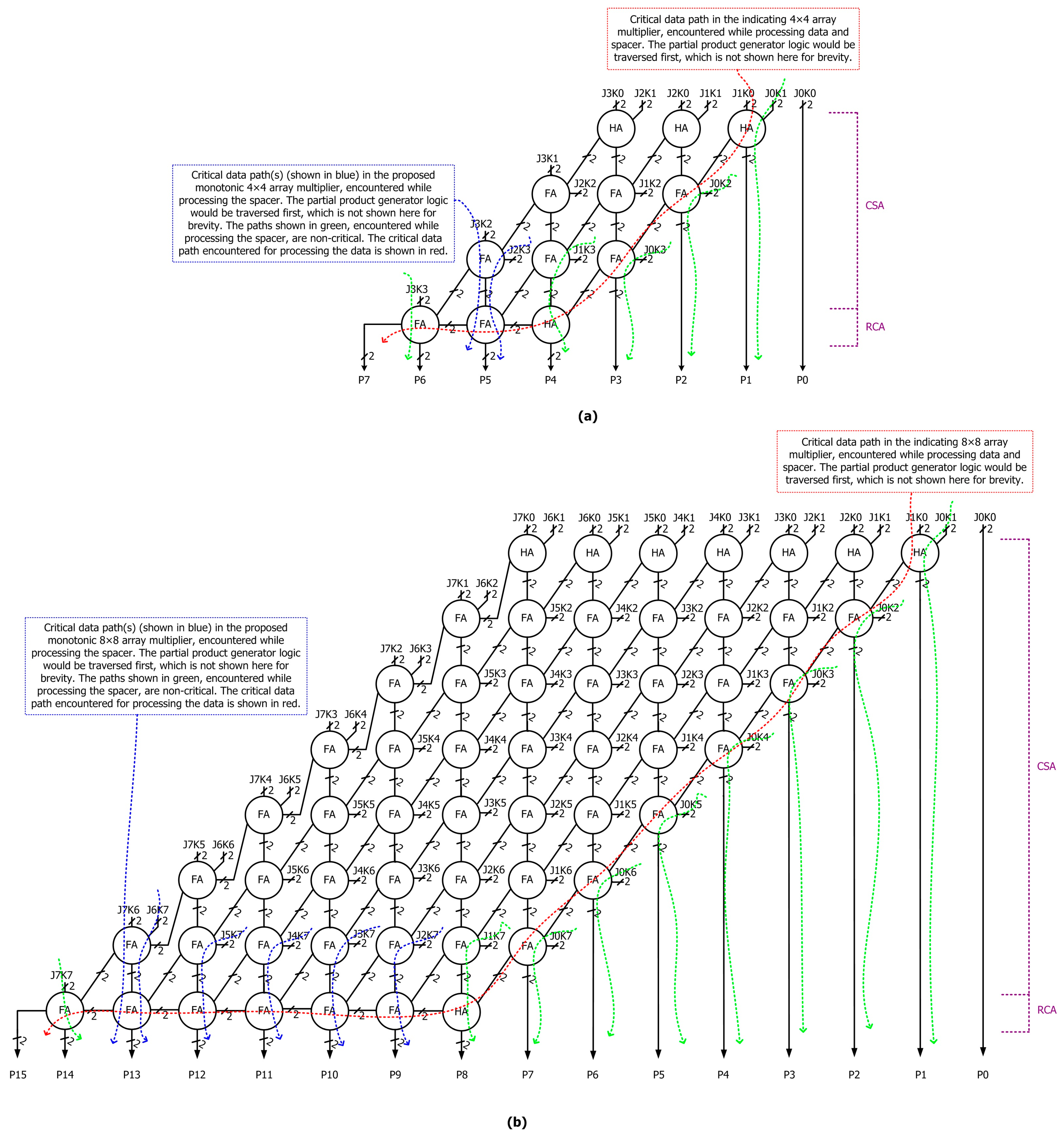
Figure 3a and b, respectively, portray the logic schematic of a 4 × 4 and an 8 × 8 array multiplier. The array multiplier implements a shift-and-add multiplication method and internally utilizes carry-save addition followed by a final-stage ripple-carry addition. The carry-save adder (CSA) and ripple-carry adder (RCA) portions of the array multipliers are highlighted with dotted violet lines in Figure 3a,b. In Figure 3a, J3 to J0 and K3 to K0 represent the multiplier inputs, with J3 and K3 being most significant and J0 and K0 being least significant. In Figure 3b, J7 to J0 and K7 to K0 represent the multiplier inputs with J7 and K7 being the most significant and J0 and K0 being the least significant. In Figure 3a,b, P7 to P0 and P15 to P0 represent the product bits, respectively, with P7 and P15 being the most significant and P0 being the least significant. In Figure 3a,b, ‘HA’ refers to the half adder, and ‘FA’ refers to the full adder. A binary half adder adds two input bits and produces the sum bit and any carry overflow. A binary full adder adds two input bits along with any carry input from a preceding stage and produces the sum bit and any carry overflow. Importantly, in Figure 3a,b, the multiplier inputs J and K are dual-rail encoded, and the multiplier output, i.e., the product P, is also dual-rail encoded. Dual-rail encoding is done according to RZH and ROH separately.
In Figure 3, ‘JxKy’ represents a partial product where x and y vary from 0 up to 3 in Figure 3a, and from 0 up to 7 in Figure 3b. An N×N array multiplier comprises N2 partial products, each of which can be synthesized using a partial product generator, N half adders, and (N2–2N) full adders. In [13], strongly indicating partial product generators were used to realize the partial products and the half adders were realized as full adders with their carry input tied to 0 with the full adders used being strongly or weakly indicating. In [14], early-output partial product generators were used to realize the partial products and strong- or weak-indication full adders were used with the half adders realized as full adders with their carry input tied to 0. In [15], early-output partial product generators, weak-indication half adders, and early-output QDI full adders were used. Among the existing works, [15] resulted in reduced design metrics while maintaining the quasi-delay insensitivity. However, there exists scope to further optimize the design metrics by adopting a non-QDI design style. To this end, we set up a monotonic asynchronous implementation of the array multiplier, particularly by implementing the building blocks monotonically, and this is the major contribution of this work. Monotonic (early-output but non-QDI) building blocks can be used to realize an IOM asynchronous array multiplier to achieve significant optimization of the design metrics. At the same time, quasi-delay insensitivity can be maintained externally for handshaking, which prevents the collision of two data wavefronts. This is because the handshake signals (AIP and AOP, shown in Figure 2) are Boolean complements of each other, and AOP is defined by the completion detector associated with the output-side register bank.
Figure 4 shows the proposed monotonic asynchronous building blocks used to realize the IOM asynchronous array multiplier. The building blocks include the partial product generator, half adder, and full adder. Figure 4a–c portray the building blocks corresponding to RZH, and Figure 4d–f portray the building blocks corresponding to ROH. To convert a logic corresponding to RZH into an equivalent logic corresponding to ROH or vice versa, all the gates except the C-element(s) therein should be replaced with their respective Boolean duals, as shown in [33]. Notably, none of the monotonic building blocks shown in Figure 4 contain the C-element in their logic, in contrast to [13,14,15]. In Figure 4, (A1, A0) and (B1, B0) represent the dual-rail inputs of the partial product generator; (P1, P0) and (Q1, Q0) represent the dual-rail inputs of the half adder; and (R1, R0), (S1, S0) and (C1, C0) represent the dual-rail inputs of the full adder. (D1, D0) represents the dual-rail encoded output of the partial product generator; (HSUM1, HSUM0) and (HCOUT1, HCOUT0) represent the dual-rail sum and carry outputs of the half adder; and (FSUM1, FSUM0) and (FCOUT1, FCOUT0) represent the dual-rail sum and carry outputs of the full adder.
We shall now explain the monotonicity and early-output nature of the proposed building blocks by considering comprehensive example scenarios corresponding to RZH. Similar example scenarios can be considered for the building blocks for ROH to comprehend their monotonicity and early-output nature, and this is left to the interest of the reader. In the following discussions, signals ‘0’ and ‘1’ are in binary format.
3.1. Partial Product Generator
Figure 4a shows the monotonic partial product generator corresponding to RZH, which implements the equations D1 = A1B1 and D0 = A0B0 + A0B1 + A1B0. When data are supplied after a spacer phase (when the primary outputs had assumed 0), if A1 and B1 assume 1, then D1 will assume 1. Alternatively, if A0 and B0 (or) A0 and B1 (or) A1 and B0 assume 1, then D0 will assume 1. Thus, all signal transitions in the partial product generator are found to be monotonically increasing (0 to 1) during data processing. Subsequently, when the spacer is supplied, even if A1 or B1 assumes 0 (if A1 and B1 were 1 earlier); A0 or B0 assumes 0 (if A0 and B0 were 1 earlier); A0 or B1 assumes 0 (if A0 and B1 were 1 earlier); or A1 or B0 assumes 0 (if A1 and B0 were 1 earlier), based on one input and regardless of the other input, D1 or D0 (whichever was 1 earlier) will assume 0. These scenarios explain the early-output and monotonically decreasing (1 to 0) nature of the partial product generator for the application of the spacer.
3.2. Half Adder
Figure 4b shows the monotonic half adder corresponding to RZH, which implements the equations HSUM1 = P0Q1 + P1Q0 and HSUM0 = P0Q0 + P1Q1, and HCOUT1 = P1Q1 and HCOUT0 = P0Q0 + P0Q1 + P1Q0. When data are supplied after a spacer phase (when the primary outputs had assumed 0), if P0 and Q1 or P1 and Q0 assume 1, then HSUM1 will assume 1. Alternatively, if P0 and Q0 or P1 and Q1 assume 1, then HSUM0 will assume 1. Likewise, if P1 and Q1 assume 1, then HCOUT1 will assume 1; alternatively, if P0 and Q0 (or) P0 and Q1 (or) P1 and Q0 assume 1, then HCOUT0 will assume 1. Hence, all signal transitions in the half adder are found to be monotonically increasing during data processing. Subsequently, when the spacer is supplied, even if P0 or Q1 assumes 0 (if P0 and Q1 were 1 earlier) or P1 or Q0 assumes 0 (if P1 and Q0 were 1 earlier), HSUM1 or otherwise HSUM0 (if it was 1 earlier) will assume 0. Likewise, even if P1 or Q1 (if P1 and Q1 were 1 earlier) assumes 0, HCOUT1 or otherwise HCOUT0 (if it was 1 earlier) will assume 0. These explain the early-output and monotonically decreasing nature of the proposed half adder for the application of the spacer.
3.3. Full Adder
Figure 4c shows the monotonic full adder corresponding to RZH, which implements the equations FSUM1 = (R0S1 + R1S0)C0 + (R0S0 + R1S1)C1 and FSUM0 = (R0S0 + R1S1)C0 + (R0S1 + R1S0)C1, and FCOUT1 = R1S1 + R1C1 + S1C1 and FCOUT0 = R0S0 + R0C0 + S0C0. When data are supplied after a spacer phase (when the primary outputs assumed 0), if R0 and S1 or R1 and S0 assume 1 and if C0 also assumes 1 (or); if R0 and S0 or R1 and S1 assume 1; and if C1 also assumes 1, then FSUM1 will assume 1; otherwise, FSUM0 will assume 1. Likewise, if R1 and S1 or R1 and C1 or S1 and C1 assume 1, FCOUT1 will assume 1; otherwise, FCOUT0 will assume 1. Therefore, all signal transitions in the full adder are found to be monotonically increasing during data processing. Subsequently, when the spacer is supplied, even if R0 or S1 or C0 assumes 0 (if R0, S1, and C0 were 1 earlier); if R1 or S0 or C0 assumes 0 (if R1, S0, and C0 were 1 earlier); if R0 or S0 or C1 assumes 0 (if R0, S0, and C1 were 1 earlier); or if R1 or S1 or C1 assumes 0 (if R1, S1, and C1 were 1 earlier), then based on just a single input assuming 0, FSUM1 could assume 0; otherwise, FSUM0 will assume 0 (if it was 1 earlier). Similarly, if R1 or S1 assumes 0 (if R1 and S1 were 1 earlier); R1 or C1 assumes 0 (if R1 and C1 were 1 earlier); or S1 or C1 assumes 0 (if S1 and C1 were 1 earlier), FCOUT1 could assume 0; otherwise, FCOUT0 will assume 0 (if it was 1 earlier). These scenarios explain the early-output and monotonically decreasing nature of the proposed full adder for the application of the spacer.
Referring to Figure 3a, which shows the schematic of the 4 × 4 array multiplier, the critical path encountered for the processing of the data (i.e., forward latency) and the spacer (i.e., reverse latency) would be the same for the existing designs [13,14,15], as highlighted by the red dotted line. Thus, the cycle time of the existing IOM asynchronous array multipliers would be twice their forward or reverse latency. This is mainly due to the use of indicating and/or early-output QDI building blocks in the existing designs. In the case of the proposed (monotonic asynchronous) array multiplier, the forward latency will be the maximum, as highlighted by the red dotted line, whereas the reverse latency will be considerably less, highlighted by the blue dotted line(s) in Figure 3a. The data paths highlighted by the green dotted lines in Figure 3a would also be traversed for the application of the spacer, but they are non-critical meaning they do not contribute to the reverse latency. As discussed earlier in Section 3.2 and Section 3.3, during the application of the spacer, the assumption of the spacer by a single corresponding input could cause the partial product generator output, the half adder outputs, and the full adder outputs to assume the spacer. Hence, in Figure 3a, all the building blocks used in the CSA (the partial product generator first, and the half adders and full adders next) would nearly simultaneously assume the spacer. Concerning the building blocks used in the RCA, they wait for inputs (spacer) from the building blocks present in only the preceding stage, i.e., the last stage of the CSA. Therefore, the reverse latency is governed by the data path(s) highlighted in blue in Figure 3a. The same explanation holds for the 8 × 8 array multiplier shown in Figure 3b, where the red dotted line highlights the forward latency and the reverse latency of the existing designs [13,14,15], while the red dotted line highlights just the forward latency of the proposed array multiplier. The reverse latency of the proposed 8 × 8 array multiplier is highlighted by the blue dotted lines in Figure 3b. In contrast, the green dotted lines indicate non-critical paths traversed for the application of the spacer.
Importantly, from Figure 3a,b, it is observed that, regardless of the multiplication size, the proposed monotonic asynchronous array multiplier tends to have a constant reverse latency that is roughly equivalent to the sum of the propagation delays of a partial product generator and two full adders. The forward latency would alone increase linearly according to the multiplication size. In contrast, for the existing IOM asynchronous array multipliers, both the forward latency and reverse latency tend to increase linearly according to the multiplication size.
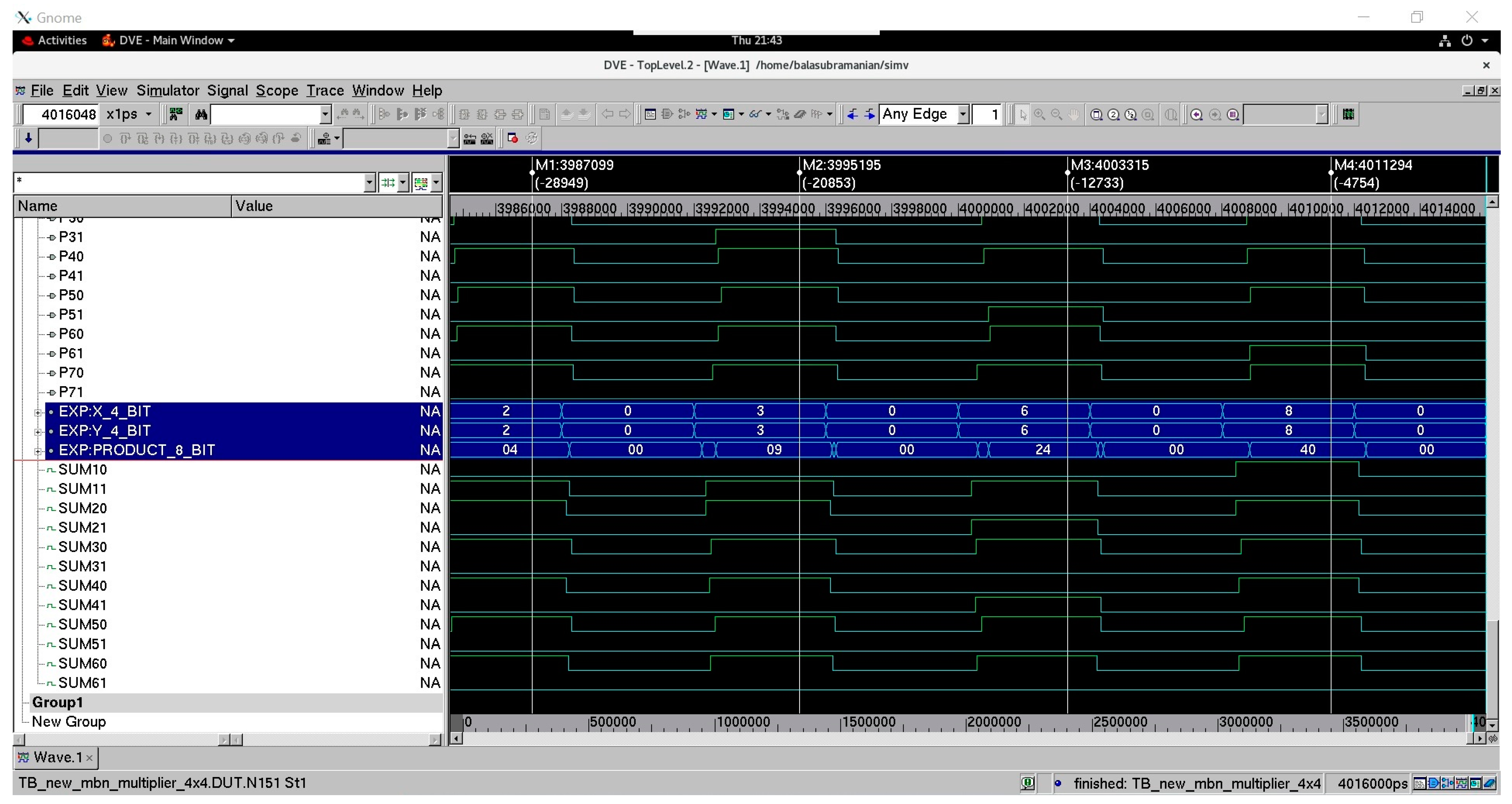
Figure 5 and Figure 6 show a screenshot of a portion of waveforms of the proposed 4 × 4 array multiplier corresponding to RZH and ROH, respectively. In Figure 5 and Figure 6, (J31, J30) up to (J01, J00) and (K31, K30) up to (K01, K00) represent two 4-bit dual-rail encoded multiplier inputs, and (P71, P70) up to (P01, P00) represents the 8-bit dual-rail encoded multiplier output. In Figure 5, the bus X_4_BIT groups the input rails (J31, J21, J11, J01) and the bus Y_4_BIT groups the input rails (K31, K21, K11, K01). The bus PRODUCT_8_BIT groups the output rails (P71, P61, P51, P41, P31, P21, P11, P01). The buses highlighted in blue in Figure 5 show example multiplications performed between the inputs and the respective product produced in hexadecimal format. The four markers M1 to M4 shown in Figure 5 point to the scenarios when some sample input data are multiplied, generating the corresponding products. It may be seen that the zero spacer separates two data products in the case of RZH, and hence the spacer product (00 H) appears between two data products. In Figure 6, the bus X_4_BIT groups the input rails (J30, J20, J10, J00) and the bus Y_4_BIT groups the input rails (K30, K20, K10, K00). The bus PRODUCT_8_BIT groups the output rails (P70, P60, P50, P40, P30, P20, P10, P00). The buses highlighted in blue in Figure 6 show example multiplications performed between the inputs and the respective product produced in hexadecimal format. The four markers M1 to M4 shown in Figure 6 point to scenarios when some sample input data are multiplied, generating the corresponding products. It may be seen that the one spacer separates two data products in the case of ROH, and hence the spacer product (ff H) appears between two data products.
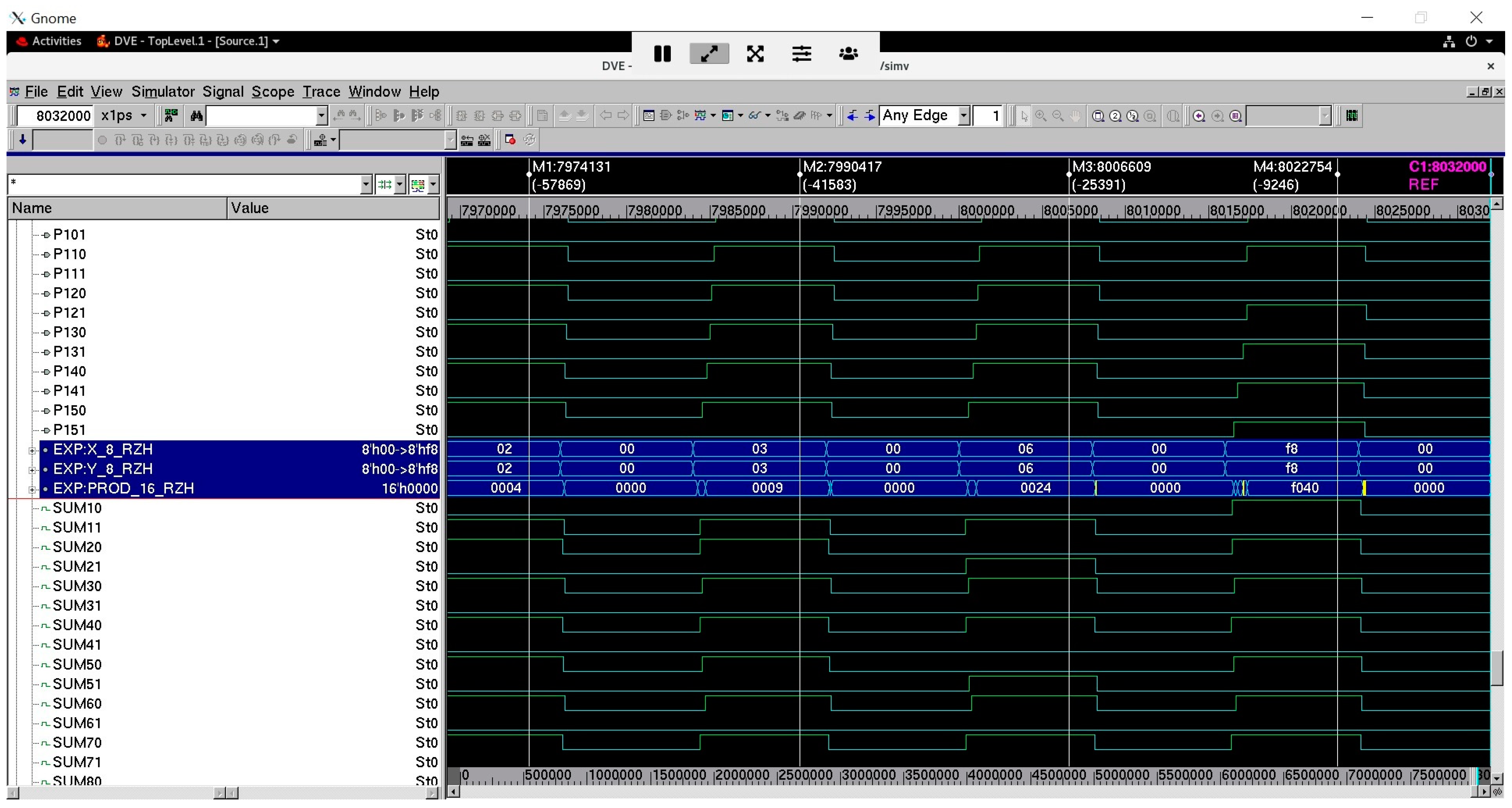
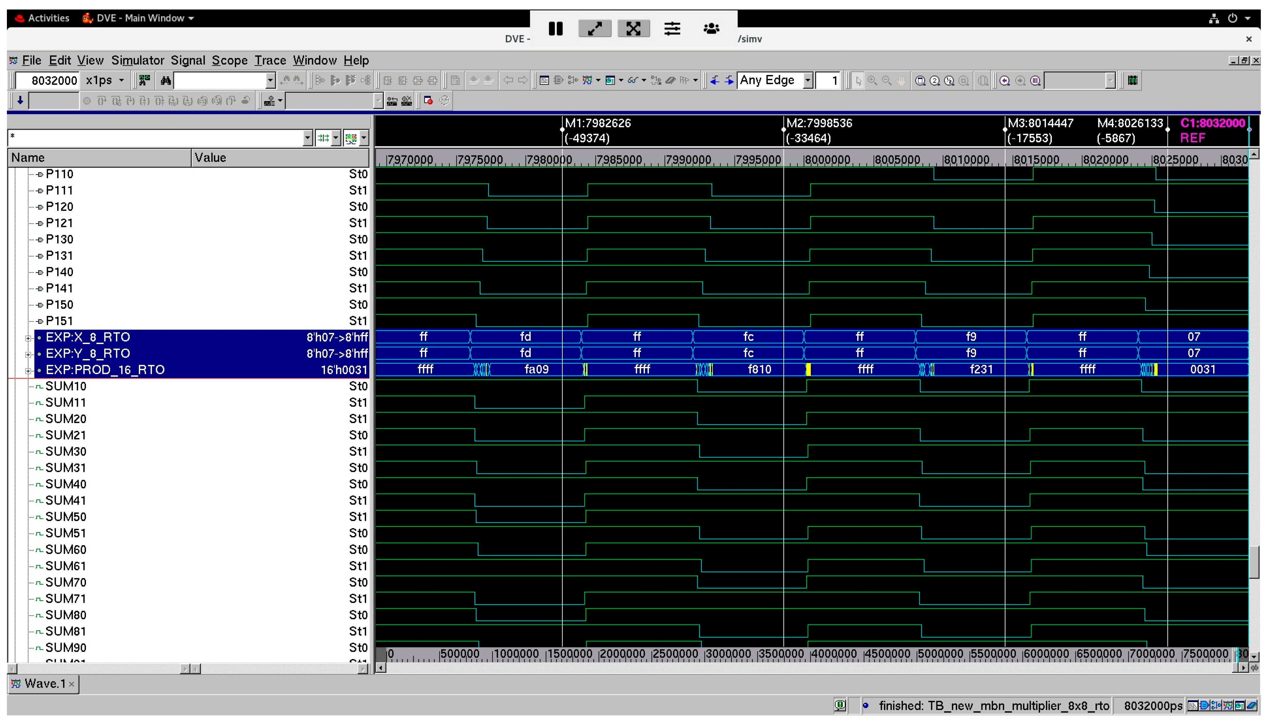
Figure 7 and Figure 8 show screenshots of a portion of waveforms of the proposed 8 × 8 array multiplier corresponding to RZH and ROH, respectively. In Figure 7 and Figure 8, (J71, J70) up to (J01, J00) and (K71, K70) up to (K01, K00) represent two 8-bit dual-rail encoded multiplier inputs, and (P151, P150) up to (P01, P00) represents the 16-bit dual-rail encoded multiplier output. In Figure 7, the bus X_8_RZH groups the input rails (J71, J61, J51, J41, J31, J21, J11, J01) and the bus Y_4_RZH groups the input rails (K71, K61, K51, K41, K31, K21, K11, K01). The bus PROD_16_RZH groups the output rails (P151, P141, P131, P121, P111, P101, P91, P81, P71, P61, P51, P41, P31, P21, P11, P01). The buses highlighted in blue in Figure 7 show example multiplications performed between the inputs and the respective product produced in hexadecimal format. The four markers M1 to M4 shown in Figure 7 point to the scenarios when some sample input data are multiplied, generating the corresponding products. It may be seen that the zero spacer separates two data products in the case of RZH, and hence the spacer product (0000 H) appears between two data products. In Figure 8, the bus X_8_RTO groups the input rails (J70, J60, J50, J40, J30, J20, J10, J00) and the bus Y_8_RTO groups the input rails (K70, K60, K50, K40, K30, K20, K10, K00). The bus PROD_16_RTO groups the output rails (P150, P140, P130, P120, P110, P100, P90, P80, P70, P60, P50, P40, P30, P20, P10, P00). The buses highlighted in blue in Figure 8 show example multiplications performed between the inputs and the respective product produced in hexadecimal format. The four markers M1 to M4 shown in Figure 8 point to the scenarios when some sample input data are multiplied, generating the corresponding products. It may be seen that the one spacer separates two data products in the case of ROH, and hence the spacer product (ffff H) appears between two data products.
4. Implementation and Design Metrics
We implemented 20 4 × 4 IOM asynchronous array multipliers, including the existing and proposed designs, with 10 corresponding to RZH and an equal number corresponding to ROH. We also implemented 20 8 × 8 IOM asynchronous array multipliers, including the existing and proposed designs, with 10 corresponding to RZH and an equal number corresponding to ROH. The 40 multipliers were realized using a 28 nm CMOS process technology [34]. It has been validated in [14] that IOM asynchronous array multipliers comprising only indicating building blocks as in [13] are inferior to their counterparts comprising a mix of indicating and early-output QDI building blocks, as in [14]. Therefore, the designs given in [13] are not considered for comparison here but the designs given in [14,15] were considered for comparison. We considered a typical case library specification that involved a supply voltage of 1.05 V and an operating temperature of 25 °C for the simulations. To perform functional simulations, approximately 2000 random input vectors were used to form test benches corresponding to 4 × 4 and 8 × 8 multiplications. The test benches contained an equal representation of data and spacers. The test benches followed a logical equivalence between RZH and ROH. The test benches were supplied to the multipliers, assuming a cycle time of 8 ns (i.e., a latency of 4 ns) for 4 × 4 multiplication, and a cycle time of 16 ns (i.e., a latency of 8 ns), aligning with prior works [13,14,15], to allow for a direct and fair comparison post-simulation. The switching activity recorded during the functional simulations was utilized to estimate the total power dissipation. A fanout-of−4 drive strength was used for all the output ports (i.e., product bits) and the default wire load was considered during the design metrics estimation. Synopsys tools were used to estimate design parameters such as the cycle time, area, and total power dissipation. The cycle time was calculated as the sum of forward latency and reverse latency. The forward latency could be estimated directly (as it is equivalent to the critical path delay of a synchronous design), and doubling the forward latency gave the cycle time of the existing designs. For the proposed designs, whose reverse latency was considerably less than the forward latency, the reverse latency was estimated based on the timing report generated by the tool. An advanced timing analysis was performed using PrimeTime, whereby a virtual clock was introduced for delay estimation, although the clock was not physically included in the designs. The design metrics of various IOM asynchronous multipliers corresponding to 4 × 4 and 8 × 8 multiplications are given in Table 1 and Table 2, respectively.
For ease of analysis and comparison, we refer to the different array multipliers using certain legends, specified in Table 1 and Table 2. The legend ‘4MZx’ generically refers to an existing 4 × 4 IOM asynchronous array multiplier corresponding to RZH with x denoting an integer value varying from 1 to 9, representing the use of a specific half adder and/or full adder from the literature. The legend ‘4Mox’ refers to the respective counterpart of ‘4MZx’, which corresponds to ROH. The legend ‘4PROPZ’ refers to the proposed 4 × 4 IOM asynchronous array multiplier corresponding to RZH, and the legend ‘4PROPO’ is the counterpart of ‘4PROPZ’ that corresponds to ROH. Likewise, the legend ‘8MZx’ generically refers to an existing 8 × 8 IOM asynchronous array multiplier corresponding to RZH, with x denoting an integer value varying from 1 to 9, representing the use of a specific half adder and/or full adder from the literature. The legend ‘8Mox’ refers to the respective counterpart of ‘8MZx’, which corresponds to ROH. The legend ‘8PROPZ’ refers to the proposed 8 × 8 IOM asynchronous array multiplier corresponding to RZH, and the legend ‘8PROPO’ is the counterpart of ‘8PROPZ’ that corresponds to ROH.
We shall now describe the components used in various IOM asynchronous array multipliers. All the IOM asynchronous array multipliers from 4MZ1 up to 4MZ8 (thus, 4MO1 up to 4MO8) and 8MZ1 up to 8MZ8 (thus, 8MO1 up to 8MO8) use the early-output partial product generator shown in Figure 4a (for RZH) and 4b (for ROH). Equally, 4MZ1 up to 4MZ8 (thus, 4MO1 up to 4MO8) and 8MZ1 up to 8MZ8 (thus, 8MO1 up to 8MO8) modify the full adder (by tying its carry input to 0) to realize the half adder functionality. Then, 4MZ1 and 8MZ1 (thus, 4MO1 and 8MO1) use the strong-indication full adder of [35]; 4MZ2 and 8MZ2 (thus, 4MO2 and 8MO2) use the strong-indication full adder of [36]; 4MZ3 and 8MZ3 (thus, 4MO3 and 8MO3) use the strong-indication full adder of [21]; 4MZ4 and 8MZ4 (thus, 4MO4 and 8MO4) use the weak-indication full adder of [36]; 4MZ5 and 8MZ5 (thus, 4MO5 and 8MO5) use the weak-indication full adder of [22]; 4MZ6 and 8MZ6 (thus, 4MO6 and 8MO6) use the weak-indication full adder of [37]; 4MZ7 and 8MZ7 (thus, 4MO7 and 8MO7) use the weak-indication full adder of [38]; and 4MZ8 and 8MZ8 (thus, 4MO8 and 8MO8) use the weak-indication SNFC full adder of [39]. Since the SNFC full adder was found to be better compared to the SN and SNX full adders of [39] in terms of the cycle time, therefore, only the SNFC full adder was considered here for comparison. In addition, 4MZ9 and 8MZ9 (thus, 4MO9 and 8MO9) use the early-output partial product generator and the weak-indication half adder depicted in [15] and the weak-indication full adder of [37]. The proposed designs 4PROPZ and 8PROPZ utilize the components shown in Figure 4a–c, and 4PROPO and 8PROPO utilize the components shown in Figure 4d–f.
From Table 1 and Table 2, it is seen that the proposed monotonic asynchronous array multipliers consume a significantly smaller area for both 4 × 4 and 8 × 8 multiplications compared to the existing QDI asynchronous array multipliers, and this is for two reasons: (i) as seen in Figure 4, the monotonic building blocks do not feature any C-element in their logic realization, and (ii) the proposed monotonic components require fewer gates and realize less complicated logic compared to the QDI realization of such components used in existing QDI asynchronous array multipliers. Among the existing designs, 4MZ9 and 8MZ9 (and 4MO9 and 8MO9) are found to be better compared to their counterparts in terms of area, cycle time, and power dissipation. However, compared to 4MZ9 and 8MZ9 (and 4MO9 and 8MO9), the proposed 4PROPZ and 8PROPZ (and 4PROPO and 8PROPO), respectively, consume a smaller area. This is mainly because the monotonic asynchronous full adders shown in Figure 4c (used in 4PROPZ and 8PROPZ) and Figure 4f (used in 4PROPO and 8PROPO) require an area of 16.77 µm2, which is 59.2% less than the weak-indication full adder of [37] used in 4MZ9 and 8MZ9 (and 4MO9 and 8MO9), which requires an area of 41.17 µm2. Also, the weakly indicating half adder [15] used in 4MZ9 and 8MZ9 (and 4MO9 and 8MO9) occupies an area of 21.35 µm2. In comparison, the monotonic half adder shown in Figure 4b,d used in 4PROPZ and 8PROPZ (and 4PROPO and 8PROPO) occupies an area of 10.42 µm2, which is 51.2% less. The early-output partial product generator [15] used in 4MZ9 and 8MZ9 (and 4MO9 and 8MO9) occupies 4.07 µm2 of area, which is 23.7% less than the area of the monotonic partial product generator used in 4PROPZ and 8PROPZ (and 4PROPO and 8PROPO), shown in Figure 4a,d, which occupies an area of 5.34 µm2. However, overall, the proposed monotonic array multiplier requires a substantially smaller area than the best of the existing QDI array multipliers. Compared to 4MZ9 (and 4MO9), 4PROPZ (and 4PROPO) consumes 37.7% less space. Compared to 8MZ9 (and 8MO9), 8PROPZ (and 8PROPO) consumes 45.2% less space. This implies that the proposed monotonic array multipliers would enable more reduction in the area compared to the existing QDI array multipliers with an increase in the multiplication size.
In terms of timing, the existing QDI array multipliers exhibit the same forward latency and reverse latency, the doubling of which results in a cycle time which would be high. The proposed monotonic array multipliers have the same forward latency as the existing QDI array multipliers, but their reverse latency is a constant roughly dictated by the sum of the propagation delays of a partial product generator and two full adders. As a result, the proposed monotonic array multipliers feature a significantly reduced cycle time compared to the existing QDI array multipliers. In Table 1, for 4 × 4 multiplication, 4PROPZ features a forward latency of 1.20 ns and a reverse latency of 0.73 ns and thus a cycle time of 1.93 ns while 4PROPO features a forward latency of 1.08 ns and a reverse latency of 0.67 ns and thus a cycle time of 1.75 ns. Thus, compared to 4MZ9, 4PROPZ achieves a 40.1% reduced cycle time, and compared to 4MO9, 4PROPO achieves a 44.3% reduced cycle time. For 8 × 8 multiplication, 8PROPZ features a forward latency of 2.41 ns and a reverse latency of 0.78 ns and thus a cycle time of 3.19 ns while 8PROPO features a forward latency of 2.18 ns and a reverse latency of 0.73 ns and thus a cycle time of 2.91 ns. Thus, compared to 8MZ9, 8PROPZ achieves a 58.1% reduced cycle time, and compared to 8MO9, 8PROPO achieves a 60.2% reduced cycle time. These imply that as the size of the multiplication increases, the proposed monotonic array multipliers will enable a greater reduction in cycle time compared to the existing QDI array multipliers since the number of logic levels containing the processing elements (such as half adders and full adders) tends to increase in linear order.
Both the existing QDI array multipliers and the proposed monotonic array multiplier adhere to the monotonic cover constraint [30], which refers to the activation of a unique signal path from the primary inputs to the primary outputs of an IOM asynchronous circuit. This is because an IOM asynchronous circuit output (corresponding to RZH) is typically expressed as a sum of disjoint products [40], where the products are mutually disjoint, and only one product term is activated corresponding to a given input data. Hence, unnecessary signal transitions do not occur widely throughout an IOM asynchronous circuit, unlike a synchronous circuit. As a result, the power dissipation does not tend to vary much between different IOM asynchronous multipliers. This contrasts with synchronous circuits where power dissipation is generally proportional to area. Therefore, in Table 1, compared to 4MZ9, 4PROPZ reports a moderate 4% decrease in power, and compared to 4MO9, 4PROPO reports a moderate 4.5% decrease in power. In Table 2, compared to 8MZ9, 8PROPZ reports a 10.3% decrease in power, and compared to 8MO9, 8PROPO reports an 11% decrease in power. Notably, the savings in power dissipation are also expected to increase with an increase in the multiplication size.
The product of power and delay commonly serves as a low-power/low-energy figure of merit in digital designs [41]. In IOM asynchronous circuits, the Power—Cycle Time Product (PCTP) serves as a low-power/low-energy figure of merit. Hence, we calculated the PCTP of all the asynchronous multipliers and normalized them. The normalization was performed by dividing the actual PCTP of each asynchronous multiplier by the highest actual PCTP of an asynchronous multiplier of the same size and corresponding to the same handshaking protocol. The results of the normalization of PCTPs of different 4 × 4 and 8 × 8 asynchronous multipliers corresponding to RZH and ROH are portrayed in Figure 9.
Since the power and cycle time should be reduced, therefore, the PCTP is also desired to be low. Therefore, in Figure 9, a PCTP of 1 implies the most inferior design and the lowest value of PCTP reflects a preferred (superior) design. From Figure 9, it is evident that the proposed monotonic asynchronous array multipliers are preferable as they exhibit reduced PCTPs compared to the existing QDI asynchronous array multipliers. Notably, for 4 × 4 multiplication, compared to 4MZ9, 4PROPZ reports a 42.5% reduction in the PCTP, and compared to 4MO9, 4PROPO reports a 46.7% reduction in the PCTP. For 8 × 8 multiplication, compared to 8MZ9, 8PROPZ reports a 62.5% reduced PCTP, and compared to 8MO9, 8PROPO reports a 64.5% reduced PCTP.
5. Conclusions
This paper has presented some monotonic asynchronous building blocks that could be used to efficiently realize monotonic asynchronous arithmetic circuits. Specifically, a monotonic partial product generator, a monotonic half adder, and a monotonic full adder were presented corresponding to RZH and ROH. When the proposed building blocks were used to realize a monotonic asynchronous array multiplier, they were found to enable significant reductions in design metrics such as the cycle time, area, and power dissipation compared to the existing QDI asynchronous array multipliers. Notably, a constant reverse latency was realized for the monotonic implementation of the asynchronous array multiplier regardless of the multiplication size, which is unlikely to be realized with existing QDI asynchronous array multipliers. The proposed monotonic asynchronous building blocks do not include the C-element in their logic realization and require fewer gates for implementation, which translates into reductions in area and power dissipation. The proposed monotonic asynchronous array multiplier achieves the following reductions in design metrics compared to the best of the existing QDI asynchronous array multipliers: (i) 40.1% (44.3%) reduction in cycle time, 37.7% (37.7%) reduction in area, and 4% (4.5%) reduction in power for 4 × 4 multiplication for RZH (ROH), and (ii) 58.1% (60.2%) reduction in cycle time, 45.2% (45.2%) reduction in area, and 10.3% (11%) reduction in power for 8 × 8 multiplication for RZH (ROH). In terms of the PCTP, which serves as a low-power/low-energy figure of merit for IOM asynchronous designs, the proposed monotonic asynchronous array multiplier consumes roughly one-half of the energy of the existing optimized QDI asynchronous array multipliers for 4 × 4 multiplication, and roughly one-third of the energy for 8 × 8 multiplication, thus suggesting an increase in energy savings with an increase in the multiplication size. Future work could consider the monotonic implementation of other building blocks such as logic compressors to realize other multipliers efficiently in a monotonic IOM asynchronous design style.
Author Contributions
Conceptualization, P.B.; methodology, P.B.; validation, P.B.; formal analysis, P.B. and N.E.M.; investigation, P.B. and N.E.M.; resources, P.B. and N.E.M.; data curation, P.B.; writing—original draft preparation, P.B.; visualization, P.B. All authors have read and agreed to the published version of the manuscript.
Funding
This research received no external funding.
Data Availability Statement
All data are available within the manuscript.
Conflicts of Interest
The authors declare no conflict of interest.
References
- Zhang, H.; Putic, M.; Lach, J. Low power GPGPU computation with imprecise hardware. In Proceedings of the 51st ACM/EDAC/IEEE Design Automation Conference, San Francisco, CA, USA, 1–5 June 2014. [Google Scholar]
- Wanhammar, L. DSP Integrated Circuits; Academic Press: Cambridge, MA, USA, 1999. [Google Scholar]
- Van Berkel, C.H.; Josephs, M.B.; Nowick, S.M. Applications of asynchronous circuits. Proc. IEEE 1999, 87, 223–233. [Google Scholar] [CrossRef]
- Martin, A.J.; Nystrom, M. Asynchronous techniques for system-on-chip design. Proc. IEEE 2006, 94, 1089–1120. [Google Scholar] [CrossRef]
- Nowick, S.M.; Singh, M. Asynchronous design—Part 1: Overview and recent advances. IEEE Des. Test 2015, 32, 5–18. [Google Scholar] [CrossRef]
- Bouesse, G.F.; Sicard, G.; Baixas, A.; Renaudin, M. Quasi delay insensitive asynchronous circuits for low EMI. In Proceedings of the 4th International Workshop on Electromagnetic Compatibility of Integrated Circuits, Angers, France, 31 March–1 April 2004. [Google Scholar]
- Yu, Z.C.; Furber, S.B.; Plana, L.A. An investigation into the security of self-timed circuits. In Proceedings of the 9th International Symposium on Advanced Research in Asynchronous Circuits and Systems, Vancouver, BC, Canada, 12–16 May 2003. [Google Scholar]
- David, I.; Ginosar, R.; Yoeli, M. Self-timed is self-checking. J. Electron. Test. Theory Appl. 1995, 6, 219–228. [Google Scholar] [CrossRef]
- Yuan, J.S.; Kuang, W. Teaching asynchronous design in digital integrated circuits. IEEE Trans. Educ. 2004, 47, 397–404. [Google Scholar] [CrossRef]
- Kim, M.M.; Kim, J.; Beckett, P. Area performance tradeoffs in NCL multipliers using two-dimensional pipelining. In Proceedings of the International SoC Design Conference, Gyungju, Republic of Korea, 2–5 November 2015. [Google Scholar]
- Metku, P.; Kim, K.K.; Kim, Y.-B.; Choi, M. Low-power null conventional logic multiplier design based on gate diffusion input technique. In Proceedings of the 15th International SoC Design Conference, Daegu, Republic of Korea, 12–15 November 2018. [Google Scholar]
- Fant, K.M.; Brandt, S.A. NULL convention logic: A complete and consistent logic for asynchronous digital circuit synthesis. In Proceedings of the International Conference on Application-Specific Systems, Architectures, and Processors, Chicago, IL, USA, 19–23 August 1996. [Google Scholar]
- Balasubramanian, P.; Maskell, D.L. Indicating asynchronous array multipliers. Int. J. Circuits Syst. Signal Process. 2019, 13, 464–471. [Google Scholar]
- Balasubramanian, P.; Maskell, D.; Naayagi, R.T.; Mastorakis, N. Early output quasi-delay-insensitive array multipliers. Electronics 2019, 8, 444. [Google Scholar] [CrossRef]
- Balasubramanian, P.; Maskell, D.L.; Mastorakis, N.E. Speed, energy and area optimized early output quasi-delay-insensitive array multipliers. PLoS ONE 2020, 15, e0228343. [Google Scholar] [CrossRef] [PubMed]
- Muller, D.E.; Bartky, S. A theory of asynchronous circuits. In Proceedings of the International Symposium on the Theory of Switching (Part I), Cambridge, MA, USA, 2–5 April 1957; Harvard University Press: Cambridge, MA, USA, 1957. [Google Scholar]
- Shams, M.; Ebergen, J.C.; Elmasry, M.I. A comparison of CMOS implementations of an asynchronous circuits primitive: The C-element. In Proceedings of the International Symposium on Low Power Electronics and Design, Monterey, CA, USA, 12–14 August 1996. [Google Scholar]
- Heck, L.S.; Moreira, M.T.; Calazans, N.L.V. Hardening C-elements against metastability. In Proceedings of the 24th IEEE International Conference on Electronics, Circuits and Systems, Batumi, Georgia, 5–8 December 2017. [Google Scholar]
- Beerel, P.A.; Ozdag, R.O.; Ferretti, M. A Designer’s Guide to Asynchronous VLSI; Cambridge University Press: Cambridge, UK, 2010. [Google Scholar]
- Seitz, C.L. System timing. In Introduction to VLSI Systems; Mead, C., Conway, L., Eds.; Addison-Wesley: Reading, MA, USA, 1980; pp. 218–262. ISBN 978-0201043587. [Google Scholar]
- Toms, W.B. Synthesis of Quasi-Delay-Insensitive Datapath Circuits. Ph.D. Thesis, The University of Manchester, Manchester, UK, 2006. [Google Scholar]
- Folco, B.; Bregier, V.; Fesquet, L.; Renaudin, M. Technology mapping for area optimized quasi delay insensitive circuits. In Proceedings of the IFIP 13th International Conference on Very Large Scale Integration, Perth, Australia, 17–19 October 2005. [Google Scholar]
- Brej, C. Early Output Logic and Anti-Tokens. Ph.D. Thesis, The University of Manchester, Manchester, UK, 2005. [Google Scholar]
- Stevens, K.S.; Ginosar, R.; Rotem, S. Relative timing. IEEE Trans. VLSI Syst. 2003, 11, 129–140. [Google Scholar] [CrossRef]
- Varshavsky, V.I. Aperiodic Circuits. In Self-Timed Control of Concurrent Processes: The Design of Aperiodic Logical Circuits in Computers and Discrete Systems; Varshavsky, V.I., Ed.; Yakovlev, A.V., Translator; Kluwer Academic Publishers: New York, NY, USA, 1990; pp. 77–85. [Google Scholar]
- Cortadella, J.; Kondratyev, A.; Lavagno, L.; Sotiriou, C. Coping with the variability of combinational logic delays. In Proceedings of the IEEE International Conference on Computer Design, San Jose, CA, USA, 11–13 October 2004. [Google Scholar]
- Martin, A.J. The limitation to delay-insensitivity in asynchronous circuits. In Beauty Is Our Business (Texts and Monographs in Computer Science); Feijen, W.H.J., van Gasteren, A.J.M., Gries, D., Misra, J., Eds.; Springer: New York, NY, USA, 1990; pp. 302–311. [Google Scholar]
- Bovik, A. Handbook of Image and Video Processing, 2nd ed.; Academic Press: Cambridge, MA, USA, 2005. [Google Scholar]
- Verhoeff, T. Delay-insensitive codes—An overview. Distrib. Comput. 1988, 3, 1–8. [Google Scholar] [CrossRef]
- Sparsø, J.; Furber, S.B. Principles of Asynchronous Circuit Design: A Systems Perspective; Kluwer Academic Publishers: Dordrecht, The Netherlands, 2001. [Google Scholar]
- Moreira, M.T.; Guazzelli, R.A.; Calazans, N.L.V. Return-to-one protocol for reducing static power in C-elements of QDI circuits employing m-of-n codes. In Proceedings of the 25th Symposium on Integrated Circuits and Systems Design, Brasilia, Brazil, 30 August–2 September 2012. [Google Scholar]
- Bose, B. On unordered codes. IEEE Trans. Comput. 1991, 40, 125–131. [Google Scholar] [CrossRef]
- Balasubramanian, P. Comparative evaluation of quasi-delay-insensitive asynchronous adders corresponding to return-to-zero and return-to-one handshaking. Facta Univ. Ser. Electron. Energetics 2018, 31, 25–39. [Google Scholar] [CrossRef]
- Synopsys SAED_EDK32/28_CORE Databook, Revision 1.0.0. January 2012. Available online: https://www.synopsys.com/community/university-program/teaching-resources.html (accessed on 7 September 2023).
- Singh, N.P. A Design Methodology for Self-Timed Systems. Master’s Thesis, Massachusetts Institute of Technology, Cambridge, MA, USA, 1981. [Google Scholar]
- Sparsø, J.; Staunstrup, J. Delay-insensitive multi-ring structures. Integration 1993, 15, 313–340. [Google Scholar] [CrossRef]
- Balasubramanian, P.; Edwards, D.A. A delay efficient robust self-timed full adder. In Proceedings of the IEEE 3rd International Design and Test Workshop, Monastir, Tunisia, 20–22 December 2008. [Google Scholar]
- Balasubramanian, P. A latency optimized biased implementation style weak-indication self-timed full adder. Facta Univ. Ser. Electron. Energetics 2015, 28, 657–671. [Google Scholar] [CrossRef]
- Huemer, F.; Steininger, A. Sorting network based full adders for QDI circuits. In Proceedings of the Austrochip Workshop on Microelectronics, Vienna, Austria, 7 October 2020. [Google Scholar]
- Sasao, T. Switching Theory for Logic Synthesis; Kluwer Academic Publishers: Dordrecht, The Netherlands, 1999; ISBN 978-1-4613-7339-1. [Google Scholar]
- Rabaey, J.M.; Chandrakasan, A.; Nikolic, B. Digital Integrated Circuits: A Design Perspective, 2nd ed.; Pearson Education: London, UK, 2003; ISBN 978-0130909961. [Google Scholar]
Figure 1.
Classification of input–output mode (IOM) asynchronous design styles.

Figure 2.
Schematic of an IOM asynchronous circuit stage showing the asynchronous circuit sandwiched between the input-side and output-side registers. Example completion detectors corresponding to return-to-zero handshaking (RZH) and return-to-one handshaking (ROH) are shown within the dotted blue and brown boxes, respectively. The circles with the marking ‘C’ represent C-elements. The critical data path traversing an input side register and the IOM asynchronous circuit is highlighted by the red dashed line. The critical data path may not be the same for the processing of data and spacer, and this depends upon the type of the IOM asynchronous circuit.

Figure 3.
Logic schematic of (a) 4 × 4 array multiplier and (b) 8 × 8 array multiplier. ‘HA’ refers to the half adder, and ‘FA’ refers to the full adder. Multiplier inputs and outputs are dual-rail encoded.
Figure 3.
Logic schematic of (a) 4 × 4 array multiplier and (b) 8 × 8 array multiplier. ‘HA’ refers to the half adder, and ‘FA’ refers to the full adder. Multiplier inputs and outputs are dual-rail encoded.

Figure 4.
Proposed monotonic building blocks used to realize the asynchronous array multiplier. (a–c) correspond to RZH; (d–f) are the logic equivalents corresponding to ROH.
Figure 4.
Proposed monotonic building blocks used to realize the asynchronous array multiplier. (a–c) correspond to RZH; (d–f) are the logic equivalents corresponding to ROH.

Figure 5.
Screenshot of a portion of simulation waveforms of the proposed 4 × 4 monotonic asynchronous array multiplier corresponding to RZH.
Figure 5.
Screenshot of a portion of simulation waveforms of the proposed 4 × 4 monotonic asynchronous array multiplier corresponding to RZH.

Figure 6.
Screenshot of a portion of simulation waveforms of the proposed 4 × 4 monotonic asynchronous array multiplier corresponding to ROH.
Figure 6.
Screenshot of a portion of simulation waveforms of the proposed 4 × 4 monotonic asynchronous array multiplier corresponding to ROH.

Figure 7.
Screenshot of a portion of simulation waveforms of the proposed 8 × 8 monotonic asynchronous array multiplier corresponding to RZH.
Figure 7.
Screenshot of a portion of simulation waveforms of the proposed 8 × 8 monotonic asynchronous array multiplier corresponding to RZH.

Figure 8.
Screenshot of a portion of simulation waveforms of the proposed 8 × 8 monotonic asynchronous array multiplier corresponding to ROH.
Figure 8.
Screenshot of a portion of simulation waveforms of the proposed 8 × 8 monotonic asynchronous array multiplier corresponding to ROH.

Figure 9.
Normalized PCTP of 4 × 4 and 8 × 8 IOM asynchronous array multipliers corresponding to RZH and ROH.
Figure 9.
Normalized PCTP of 4 × 4 and 8 × 8 IOM asynchronous array multipliers corresponding to RZH and ROH.


Table 1.
Design metrics of 4 × 4 IOM asynchronous array multipliers.
| Multiplier Legend | Area (µm2) | Cycle Time (ns) | Power (µW) |
|---|---|---|---|
| Corresponding to return-to-zero handshaking (RZH) | |||
| 4MZ1 *α | 852.65 | 7.18 | 706.5 |
| 4MZ2 *α | 843.50 | 5.34 | 686.9 |
| 4MZ3 *α | 764.21 | 5.78 | 676.7 |
| 4MZ4 *β | 813.01 | 5.12 | 681.8 |
| 4MZ5 *β | 660.52 | 5.10 | 675.3 |
| 4MZ6 *β | 691.02 | 3.82 | 681.1 |
| 4MZ7 *β | 672.72 | 4.40 | 675.7 |
| 4MZ8 *β | 785.56 | 5.36 | 707.5 |
| 4MZ9 *βγ | 579.45 | 3.22 | 586.3 |
| 4PROPZ ψ | 360.88 | 1.93 | 562.6 |
| Corresponding to return-to-one handshaking (ROH) | |||
| 4MO1 *α | 852.65 | 6.96 | 705.2 |
| 4MO2 *α | 794.71 | 5.06 | 676.2 |
| 4MO3 *α | 764.21 | 5.66 | 679.4 |
| 4MO4 *β | 788.61 | 4.92 | 675.9 |
| 4MO5 *β | 660.52 | 5.00 | 674.8 |
| 4MO6 *β | 691.02 | 3.58 | 680.6 |
| 4MO7 *β | 672.72 | 4.26 | 676.2 |
| 4MO8 *β | 785.56 | 5.26 | 714.2 |
| 4MO9 *βγ | 579.45 | 3.14 | 586.7 |
| 4PROPO ψ | 360.88 | 1.75 | 560.3 |
* Partial product generator is of the early-output type; α Full adder is of strong-indication type; β Full adder is of weak-indication type; γ Half adder is of weak-indication type; ψ Partial product generator, half adder, and full adder are monotonic (early-output) type.
Table 2.
Design metrics of 8 × 8 IOM asynchronous array multipliers.
| Multiplier Legend | Area (µm2) | Cycle Time (ns) | Power (µW) |
|---|---|---|---|
| Corresponding to return-to-zero handshaking (RZH) | |||
| 8MZ1 *α | 3608.58 | 14.38 | 910.0 |
| 8MZ2 *α | 3565.89 | 10.94 | 860.1 |
| 8MZ3 *α | 3195.86 | 11.78 | 834.1 |
| 8MZ4 *β | 3423.57 | 10.40 | 848.1 |
| 8MZ5 *β | 2711.97 | 10.18 | 827.9 |
| 8MZ6 *β | 2854.29 | 8.26 | 842.2 |
| 8MZ7 *β | 2768.90 | 8.52 | 828.4 |
| 8MZ8 *β | 3295.48 | 11.20 | 910.2 |
| 8MZ9 *βγ | 2602.44 | 7.62 | 779.6 |
| 8PROPZ ψ | 1425.24 | 3.19 | 699.6 |
| Corresponding to return-to-one handshaking (ROH) | |||
| 8MO1 *α | 3608.58 | 13.96 | 906.9 |
| 8MO2 *α | 3338.18 | 10.36 | 835.4 |
| 8MO3 *α | 3195.86 | 11.58 | 838.9 |
| 8MO4 *β | 3309.71 | 10.04 | 834.2 |
| 8MO5 *β | 2711.97 | 10.00 | 826.5 |
| 8MO6 *β | 2854.29 | 7.82 | 841.4 |
| 8MO7 *β | 2768.90 | 8.30 | 829.3 |
| 8MO8 *β | 3295.48 | 11.10 | 921.7 |
| 8MO9 *βγ | 2602.44 | 7.32 | 780.7 |
| 8PROPO ψ | 1425.24 | 2.91 | 694.9 |
* Partial product generator is of the early-output type; α Full adder is of strong-indication type; β Full adder is of weak-indication type; γ Half adder is of weak-indication type; ψ Partial product generator, half adder, and full adder are monotonic (early-output) type.
Disclaimer/Publisher’s Note: The statements, opinions and data contained in all publications are solely those of the individual author(s) and contributor(s) and not of MDPI and/or the editor(s). MDPI and/or the editor(s) disclaim responsibility for any injury to people or property resulting from any ideas, methods, instructions or products referred to in the content. |
© 2023 by the authors. Licensee MDPI, Basel, Switzerland. This article is an open access article distributed under the terms and conditions of the Creative Commons Attribution (CC BY) license (https://creativecommons.org/licenses/by/4.0/).
Share and Cite
MDPI and ACS Style
Balasubramanian, P.; Mastorakis, N.E. Speed, Power and Area Optimized Monotonic Asynchronous Array Multipliers. J. Low Power Electron. Appl. 2024, 14, 1. https://doi.org/10.3390/jlpea14010001
AMA Style
Balasubramanian P, Mastorakis NE. Speed, Power and Area Optimized Monotonic Asynchronous Array Multipliers. Journal of Low Power Electronics and Applications. 2024; 14(1):1. https://doi.org/10.3390/jlpea14010001
Chicago/Turabian StyleBalasubramanian, Padmanabhan, and Nikos E. Mastorakis. 2024. "Speed, Power and Area Optimized Monotonic Asynchronous Array Multipliers" Journal of Low Power Electronics and Applications 14, no. 1: 1. https://doi.org/10.3390/jlpea14010001
Note that from the first issue of 2016, this journal uses article numbers instead of page numbers. See further details here.