Next Issue
Volume 14, June
Previous Issue
Volume 13, December


J. Low Power Electron. Appl., Volume 14, Issue 1 (March 2024) – 17 articles

Cover Story (view full-size image): 
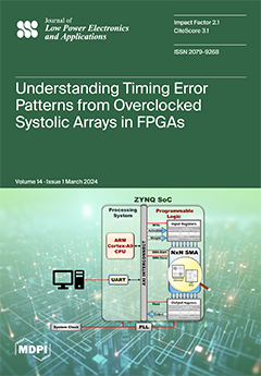
Many AI hardware accelerators comprise a systolic multiply–accumulate array (SMA) as its computational brain. We investigate the faulty output characterization of an SMA in a real silicon FPGA board. Our extensive experimental platform with a hardware–software ecosystem provides a methodological pathway that reveals fascinating characteristics of SMA behavior in an overclocked environment. While one may intuitively expect that timing errors resulting from overclocked hardware may produce a wide variation in output values, our post-silicon evaluation reveals a lack of variation in erroneous output values. We found an intriguing pattern where error output values are stable for a given input across a range of operating frequencies far exceeding the rated frequency of the FPGA. View this paper
  • Issues are regarded as officially published after their release is announced to the table of contents alert mailing list.
  • You may sign up for e-mail alerts to receive table of contents of newly released issues.
  • PDF is the official format for papers published in both, html and pdf forms. To view the papers in pdf format, click on the "PDF Full-text" link, and use the free Adobe Reader to open them.
Order results
Result details
Select all
Export citation of selected articles as:
14 pages, 1090 KiB  
Article
A Simplified GmC Filter Technique for Reference Spur Reduction in Phase-Locked Loop
by P. Purushothama Chary, Rizwan Shaik Peerla and Ashudeb Dutta
J. Low Power Electron. Appl. 2024, 14(1), 17; https://doi.org/10.3390/jlpea14010017 - 20 Mar 2024
Viewed by 850
Abstract
This paper presents a wideband approach for L5 and S-band integer-N phase-locked loop (PLL) targeting Indian Regional Navigation Satellite System (IRNSS) applications. A reference spur reduction technique using a GmC filter is proposed. The reference spur is improved by 7 [...] Read more.
This paper presents a wideband approach for L5 and S-band integer-N phase-locked loop (PLL) targeting Indian Regional Navigation Satellite System (IRNSS) applications. A reference spur reduction technique using a GmC filter is proposed. The reference spur is improved by 7 dB when compared with one without any GmC filter. The wideband integer-N PLL is designed and fabricated in UMC 65-nm CMOS process. The GmC filter block consumes 200 μA current. The wideband voltage-controlled oscillator (VCO) oscillates from 1.6 GHz to 3.2 GHz having a tuning range (TR) of 40%, achieving a best and worst phase noise of ≈−122 dBc/Hz and ≈116 dBc/Hz at a 1 MHz offset, respectively. Full article
Show Figures

Figure 1

11 pages, 1933 KiB  
Communication
Design of Impedance Matching Network for Low-Power, Ultra-Wideband Applications
by Sepideh Hassani, Chih-Hung Chen and Natalia K. Nikolova
J. Low Power Electron. Appl. 2024, 14(1), 16; https://doi.org/10.3390/jlpea14010016 - 19 Mar 2024
Viewed by 883
Abstract
This paper addresses the design of ultra-wideband (UWB) impedance matching networks operating in the unlicensed 3.1–10.6 GHz frequency band for low-power applications. It improves the simplified real frequency technique (SRFT) by adding a realizability check and employing an iterative approach with different initial [...] Read more.
This paper addresses the design of ultra-wideband (UWB) impedance matching networks operating in the unlicensed 3.1–10.6 GHz frequency band for low-power applications. It improves the simplified real frequency technique (SRFT) by adding a realizability check and employing an iterative approach with different initial guesses in optimization to achieve realizable solutions under the requirements of UWB, low-power consumption, and a minimum number of circuit components. The comparison of solutions obtained using the SRFT with published solutions based on the Chebyshev filter theory is presented. It is shown that the optimal SRFT solution requires fewer components in the impedance matching network, maximizes the RF power delivery over the UWB spectrum with a reflection coefficient below −10 dB, and allows for circuit optimization to reduce power consumption. Using the improved SRFT, it demonstrates a systematic approach to find the strategies and limitations of designing the input matching networks for low-power UWB applications using GlobalFoundries 90 nm BiCMOS technology. Full article
Show Figures

Figure 1

16 pages, 3134 KiB  
Article
Control of Vibratory Feeder Device Mechanical Frequency Using the Modification of the Sinusoidal Supply Voltage Signal
by Žydrūnas Kavaliauskas and Igor Šajev
J. Low Power Electron. Appl. 2024, 14(1), 15; https://doi.org/10.3390/jlpea14010015 - 06 Mar 2024
Viewed by 1141
Abstract
In the industrial and sales processes, dosing systems of various constructions, whose operation is based on mechanical vibrations (vibratory feeders), are very often used. These systems face many problems, such as resonant frequency, flow instability of dosed product, instability of mechanical vibration amplitude, [...] Read more.
In the industrial and sales processes, dosing systems of various constructions, whose operation is based on mechanical vibrations (vibratory feeders), are very often used. These systems face many problems, such as resonant frequency, flow instability of dosed product, instability of mechanical vibration amplitude, etc., because most of them are based on controlling the frequency of the electrical signal of the supply voltage. All these factors negatively affect the durability and reliability of the vibratory feeder systems. During this research, an automatic control system for vibratory feeder was created, whose control process is based on the modification of the sinusoidal signal (partially changing the signal area). In addition, such a way of controlling the vibratory feeder is not discussed in the literature. As the research conducted in this paper has shown, while using sinusoidal signal modification it was possible to achieve a stable flow rate of bulk production (the flow rate varied from 0 to 100 g/s when the frequency of mechanical vibrations changed from 1 to 50 Hz) and a stable amplitude of mechanical oscillations was achieved and equal to 1.5 mm. The control system is based on the microcontroller PIC24FV32KA302 for which the special software was developed. The thyristor BTA16 used for voltage modification of the sinusoidal signal made it possible to ensure the reliable control of the sinusoidal voltage modification process. Full article
Show Figures

Figure 1

17 pages, 4705 KiB  
Article
CMOS Design of Chaotic Systems Using Biquadratic OTA-C Filters
by Eduardo Juarez-Mendoza, Francisco Asahel del Angel-Diaz, Alejandro Diaz-Sanchez and Esteban Tlelo-Cuautle
J. Low Power Electron. Appl. 2024, 14(1), 14; https://doi.org/10.3390/jlpea14010014 - 04 Mar 2024
Viewed by 1429
Abstract
This manuscript shows the CMOS design of Lorenz systems using operational transconductance amplifiers (OTAs). Two Lorenz systems are then synchronized in a master–slave topology and used to implement a CMOS secure communication system. The contribution is devoted to the correct design of first- [...] Read more.
This manuscript shows the CMOS design of Lorenz systems using operational transconductance amplifiers (OTAs). Two Lorenz systems are then synchronized in a master–slave topology and used to implement a CMOS secure communication system. The contribution is devoted to the correct design of first- and second-order OTA-C filters, using 180 nm CMOS technology, to guarantee chaotic behavior. First, Simulink is used to simulate a secure communication system using two Lorenz systems connected in a master–slave topology, which is tested using sinusoidal signals that are masked by chaotic signals. Second, the Lorenz systems are scaled to have amplitudes of the state variables below 1 Volt, to allow for CMOS design using OTA-C filters. The transconductances of the OTAs are tuned to accomplish a Laplace transfer function. In this manner, this work highlights the design of a second-order CMOS OTA-C filter, whose damping factor is tuned to generate appropriate chaotic behavior. Finally, chaotic masking is performed by designing a whole CMOS secure communication system by using OTA-C based Lorenz systems, and its SPICE simulation results show its appropriateness for hardware security applications. Full article
Show Figures

Figure 1

17 pages, 2747 KiB  
Article
A Sub-1-V Nanopower MOS-Only Voltage Reference
by Siqi Wang, Zhenghao Lu, Kunpeng Xu, Hongguang Dai, Zhanxia Wu and Xiaopeng Yu
J. Low Power Electron. Appl. 2024, 14(1), 13; https://doi.org/10.3390/jlpea14010013 - 29 Feb 2024
Viewed by 1139
Abstract
A novel low-power MOS-only voltage reference is presented. The Enz–Krummenacher–Vittoz (EKV) model is adopted to provide a new perspective on the operating principle. The normalized charge density, introduced as a new variable, serves as an indicator when trimming the output temperature coefficient. The [...] Read more.
A novel low-power MOS-only voltage reference is presented. The Enz–Krummenacher–Vittoz (EKV) model is adopted to provide a new perspective on the operating principle. The normalized charge density, introduced as a new variable, serves as an indicator when trimming the output temperature coefficient. The proposed voltage reference consists of a specific current generator and a 5-bit trimmable load. Thanks to the good match between the current source stage and the output stage, the nonlinear temperature dependence of carrier mobility is automatically canceled out. The circuit is designed using 55 nm COMS technology. The operating temperature ranges from −40 °C to 120 °C. The average temperature coefficient of the output voltage can be reduced to 21.7 ppm/°C by trimming. The power consumption is only 23.2 nW with a supply voltage of 0.8 V. The line sensitivity and the power supply rejection ratio at 100 Hz are 0.011 %/V and −89 dB, respectively. Full article
(This article belongs to the Special Issue Ultra-Low-Power ICs for the Internet of Things Vol. 2)
Show Figures

Figure 1

16 pages, 8901 KiB  
Article
A Low-Power BL Path Design for NAND Flash Based on an Existing NAND Interface
by Hikaru Makino and Toru Tanzawa
J. Low Power Electron. Appl. 2024, 14(1), 12; https://doi.org/10.3390/jlpea14010012 - 19 Feb 2024
Viewed by 1304
Abstract
This paper is an extended version of a previously reported conference paper regarding a low-power design for NAND Flash. As the number of bits per NAND Flash die increases with cost scaling, the IO data path speed increases to minimize the page access [...] Read more.
This paper is an extended version of a previously reported conference paper regarding a low-power design for NAND Flash. As the number of bits per NAND Flash die increases with cost scaling, the IO data path speed increases to minimize the page access time with a scaled CMOS in IOs. The power supply for IO buffers, namely, VDDQ, decreases from 3 V to 1.2 V, accordingly. In this paper, the way in which a reduction in VDDQ can contribute to power reduction in the BL path is discussed and validated. Conventionally, a BL voltage of about 0.5 V has been supplied from a supply voltage source (VDD) of 3 V. The BL path power can be reduced by a factor of VDDQ to VDD when the BL voltage is supplied by VDDQ. To maintain a sense margin at the sense amplifiers, the supply source for BLs is switched from VDDQ to VDD before sensing. As a result, power reduction and an equivalent sense margin can be realized at the same time. The overhead of implementing this operation is an increase in the BL access time of about 2% for switching the power supply from VDDQ to VDD and an increase in the die size of about 0.01% for adding the switching circuit, both of which are not significant in comparison to the significant power reduction in the BL path power of the NAND die of about 60%. The BL path is then designed in 180 nm CMOS to validate the design. When the cost for powering the SSD becomes quite significant, especially for data centers, an additional lower voltage supply, such as 0.8 V, dedicated to BL charging for read and program verifying operations may be the best option for future applications. Full article
Show Figures

Figure 1

16 pages, 9834 KiB  
Article
Extrema-Triggered Conversion for Non-Stationary Signal Acquisition in Wireless Sensor Nodes
by Swagat Bhattacharyya and Jennifer O. Hasler
J. Low Power Electron. Appl. 2024, 14(1), 11; https://doi.org/10.3390/jlpea14010011 - 17 Feb 2024
Viewed by 1268
Abstract
While wireless sensor node (WSNs) have proliferated with the rise of the Internet of Things (IoT), uniformly sampled analog–digital converters (ADCs) have traditionally reigned paramount in the signal processing pipeline. The large volume of data generated by uniformly sampled ADCs while capturing most [...] Read more.
While wireless sensor node (WSNs) have proliferated with the rise of the Internet of Things (IoT), uniformly sampled analog–digital converters (ADCs) have traditionally reigned paramount in the signal processing pipeline. The large volume of data generated by uniformly sampled ADCs while capturing most real-world signals, which are highly non-stationary and sparse in information content, considerably strains the power budget of WSNs during data transmission. Given the pressing need for intelligent sampling, this work proposes an extrema pulse generator devised to trigger ADCs at significant signal extrema, thereby curbing the volume of data points collected and transmitted, and mitigating transmission power draw. After providing a comprehensive signal-theoretic rationale, we construct and experimentally validate these circuits on a system-on-chip field-programmable analog array in a 350 nm complementary metal-oxide-semiconductor (MOS) process. Operating within a power range of 4.3–12.3 µW (contingent on the input bandwidth requirements), the extrema pulse generator has proven to be capable of effectively sampling both synthetic and natural signals, achieving significant reductions in data volume and signal reconstruction error. Using a nonideality-resilient reconstruction algorithm, that we develop in this work, experimental comparisons between extrema and uniform sampling show that extrema sampling achieves an 18-fold lower normalized root mean square reconstruction error for a quadratic chirp signal, despite requiring 5-fold fewer sample points. Similar improvements in both the reconstruction error and effective sampling rate objectives are found experimentally for an electrocardiogram signal. Using both theoretical and experimental methods, this work demonstrates the potential of extrema-triggered systems for extending Pareto frontiers in modern, resource-constrained sensing scenarios. Full article
Show Figures

Figure 1

23 pages, 5373 KiB  
Article
PANDA: Processing in Magnetic Random-Access Memory-Accelerated de Bruijn Graph-Based DNA Assembly
by Shaahin Angizi, Naima Ahmed Fahmi, Deniz Najafi, Wei Zhang and Deliang Fan
J. Low Power Electron. Appl. 2024, 14(1), 9; https://doi.org/10.3390/jlpea14010009 - 02 Feb 2024
Viewed by 1636
Abstract
In this work, we present an efficient Processing in MRAM-Accelerated De Bruijn Graph-based DNA Assembly platform, named PANDA, based on an optimized and hardware-friendly genome assembly algorithm. PANDA is able to assemble large-scale DNA sequence datasets from all-pair overlaps. We first design a [...] Read more.
In this work, we present an efficient Processing in MRAM-Accelerated De Bruijn Graph-based DNA Assembly platform, named PANDA, based on an optimized and hardware-friendly genome assembly algorithm. PANDA is able to assemble large-scale DNA sequence datasets from all-pair overlaps. We first design a PANDA platform that exploits MRAM as computational memory and converts it to a potent processing unit for genome assembly. PANDA can not only execute efficient bulk bit-wise X(N)OR-based comparison/addition operations heavily required for the genome assembly task but also a full set of 2-/3-input logic operations inside the MRAM chip. We then develop a highly parallel and step-by-step hardware-friendly DNA assembly algorithm for PANDA that only requires the developed in-memory logic operations. The platform is then configured with a novel data partitioning and mapping technique that provides local storage and processing to utilize the algorithm level’s parallelism fully. The cross-layer simulation results demonstrate that PANDA reduces the run time and power by a factor of 18 and 11, respectively, compared with CPU. Moreover, speed-ups of up to 2.5 to 10× can be obtained over other recent processing in-memory platforms to perform the same task, like STT-MRAM, ReRAM, and DRAM. Full article
Show Figures

Figure 1

18 pages, 12954 KiB  
Article
A Low-Power, 65 nm 24.6-to-30.1 GHz Trusted LC Voltage-Controlled Oscillator Achieving 191.7 dBc/Hz FoM at 1 MHz
by Abdullah Kurtoglu, Amir H. M. Shirazi, Shahriar Mirabbasi and Hossein Miri Lavasani
J. Low Power Electron. Appl. 2024, 14(1), 10; https://doi.org/10.3390/jlpea14010010 - 02 Feb 2024
Viewed by 1462
Abstract
This work presents a novel trusted LC voltage-controlled oscillator (VCO) with an embedded compact analog Physically Unclonable Function (PUF) used for authentication. The trusted VCO is implemented in a 1P9M 65 nm standard CMOS process and consumes 1.75 mW. It exhibits a measured [...] Read more.
This work presents a novel trusted LC voltage-controlled oscillator (VCO) with an embedded compact analog Physically Unclonable Function (PUF) used for authentication. The trusted VCO is implemented in a 1P9M 65 nm standard CMOS process and consumes 1.75 mW. It exhibits a measured phase noise (PN) of −104.8 dBc/Hz @ 1 MHz and −132.2 dBc/Hz @ 10 MHz offset, resulting in Figures of Merit (FoMs) of 191.7 dBc/Hz and 199.1 dBc/Hz, respectively. With the measured frequency tuning range (TR) of ~5.5 GHz, the FoM with tuning (FoMT) reaches 197.6 dBc/Hz and 205.0 dBc/Hz at 1 MHz and 10 MHz offset, respectively. The analog PUF consists of CMOS cross-coupled pairs in the main VCO to change analog characteristics. Benefiting from the impedance change and parasitic capacitance of the cross-coupled pairs, the AC and DC responses of the VCO are utilized for multiple responses for each input. The PUF consumes 0.83 pJ/bit when operating at 1.5 Gbps. The proposed PUF exhibits a measured Inter-Hamming Distance (HD) of 0.5058b and 0.4978b, with Intra-HD reaching 0.0055b and 0.0053b for the current consumption and fosc, respectively. The autocorrelation function (ACF) of 0.0111 and 0.0110 is obtained for the current consumption and fosc, respectively, at a 95% confidence level. Full article
Show Figures

Figure 1

17 pages, 6203 KiB  
Article
LC Tank Oscillator Based on New Negative Resistor in FDSOI Technology
by Yuqing Mao, Yoann Charlon, Yves Leduc and Gilles Jacquemod
J. Low Power Electron. Appl. 2024, 14(1), 8; https://doi.org/10.3390/jlpea14010008 - 01 Feb 2024
Cited by 1 | Viewed by 1448
Abstract
Although Moore’s Law reaches its limits, it has never applied to analog and RF circuits. For example, due to the short channel effect (SCE), drain-induced barrier lowering (DIBL), and sub-threshold slope (SS)…, longer transistors are required to implement analog cells. From 22 nm [...] Read more.
Although Moore’s Law reaches its limits, it has never applied to analog and RF circuits. For example, due to the short channel effect (SCE), drain-induced barrier lowering (DIBL), and sub-threshold slope (SS)…, longer transistors are required to implement analog cells. From 22 nm CMOS technology and beyond, for reasons of variability, the channel of the transistors has no longer been doped. Two technologies then emerged: FinFET transistors for digital applications and UTBB FDSOI transistors, suitable for analog and mixed applications. In a previous paper, a new topology was proposed utilizing some advantages of the FDSOI technology. Thanks to this technology, a novel cross-coupled back-gate (BG) technique was implemented to improve analog and mixed signal cells in order to reduce the surface of the integrated circuit. This technique was applied to a current mirror to reduce the small channel effect and to provide high-output impedance. It was demonstrated that it is possible to overcompensate the SCE and DIBL effects and to create a negative output resistor. This paper presents a new LC tank oscillator based on this current mirror functioning as a negative resistor. Full article
Show Figures

Figure 1

24 pages, 7423 KiB  
Review
Array-Designed Triboelectric Nanogenerator for Healthcare Diagnostics: Current Progress and Future Perspectives
by Zequan Zhao, Qiliang Zhu, Yifei Wang, Muhammad Shoaib, Xia Cao and Ning Wang
J. Low Power Electron. Appl. 2024, 14(1), 7; https://doi.org/10.3390/jlpea14010007 - 22 Jan 2024
Viewed by 1722
Abstract
Array-designed triboelectric nanogenerators (AD-TENGs) have firmly established themselves as state-of-the-art technologies for adeptly converting mechanical interactions into electrical signals. Central to the AD-TENG’s prowess is its inherent modularity and the multifaceted, grid-like design that pave the way to robust and adaptable detection platforms [...] Read more.
Array-designed triboelectric nanogenerators (AD-TENGs) have firmly established themselves as state-of-the-art technologies for adeptly converting mechanical interactions into electrical signals. Central to the AD-TENG’s prowess is its inherent modularity and the multifaceted, grid-like design that pave the way to robust and adaptable detection platforms for wearables and real-time health monitoring systems. In this review, we aim to elucidate the quintessential role of array design in AD-TENGs for healthcare detection, emphasizing its ability to heighten sensitivity, spatial resolution, and dynamic monitoring while ensuring redundancy and simultaneous multi-detection. We begin from the fundamental aspects, such as working principles and design basis, then venture into methodologies for optimizing AD-TENGs that ensure the capture of intricate physiological changes, from nuanced muscle movements to sensitive electronic skin. After this, our exploration extends to the possible cutting-edge electronic systems that are built with specific advantages in filtering noise, magnifying signal-to-noise ratios, and interpreting complex real-time datasets on the basis of AD-TENGs. Culminating our discourse, we highlight the challenges and prospective pathways in the evolution of array-designed AD-TENGs, stressing the necessity to refine their sensitivity, adaptability, and reliability to perfectly align with the exacting demands of contemporary healthcare diagnostics. Full article
Show Figures

Figure 1

18 pages, 5415 KiB  
Article
Advancing Smart Lighting: A Developmental Approach to Energy Efficiency through Brightness Adjustment Strategies
by Vandha Pradwiyasma Widartha, Ilkyeun Ra, Su-Yeon Lee and Chang-Soo Kim
J. Low Power Electron. Appl. 2024, 14(1), 6; https://doi.org/10.3390/jlpea14010006 - 15 Jan 2024
Viewed by 2162
Abstract
Smart lighting control systems represent an advanced approach to reducing energy use. These systems leverage advanced technology to provide users with better control over their lighting, allowing them to manually, remotely, and automatically modify the brightness, color, and timing of their lights. In [...] Read more.
Smart lighting control systems represent an advanced approach to reducing energy use. These systems leverage advanced technology to provide users with better control over their lighting, allowing them to manually, remotely, and automatically modify the brightness, color, and timing of their lights. In this study, we aimed to enhance the energy efficiency of smart lighting systems by using light source data. A multifaceted approach was employed, involving the following three scenarios: sensing device, daylight data, and a combination of both. A low-cost sensor and third-party API were used for data collection, and a prototype application was developed for real-time monitoring. The results showed that combining sensor and daylight data effectively reduced energy consumption, and the rule-based algorithm further optimized energy usage. The prototype application provided real-time monitoring and actionable insights, thus contributing to overall energy optimization. Full article
Show Figures

Figure 1

24 pages, 2686 KiB  
Article
A Scalable Formal Framework for the Verification and Vulnerability Analysis of Redundancy-Based Error-Resilient Null Convention Logic Asynchronous Circuits
by Dipayan Mazumder, Mithun Datta, Alexander C. Bodoh and Ashiq A. Sakib
J. Low Power Electron. Appl. 2024, 14(1), 5; https://doi.org/10.3390/jlpea14010005 - 14 Jan 2024
Viewed by 1573
Abstract
The increasing demand for high-speed, energy-efficient, and miniaturized electronics has led to significant challenges and compromises in the domain of conventional clock-based digital designs, most notably reduced circuit reliability, particularly in mission-critical hardware. At scaled technology nodes, devices are vulnerable to transient or [...] Read more.
The increasing demand for high-speed, energy-efficient, and miniaturized electronics has led to significant challenges and compromises in the domain of conventional clock-based digital designs, most notably reduced circuit reliability, particularly in mission-critical hardware. At scaled technology nodes, devices are vulnerable to transient or soft errors, such as Single Event Upset (SEU) and Single Event Latch-up (SEL). External radiation, internal electromagnetic interference (EMI), or noise are the primary sources of these errors, which can compromise the circuit functionality. In response to these challenges, the Quasi-Delay-Insensitive (QDI) Null Convention Logic (NCL) asynchronous design paradigm has emerged as a promising alternative, offering advantages such as ultra-low power performance, reduced noise and EMI, and resilience to process, voltage, and temperature variations. Moreover, its unique architecture and insensitivity to timing variations offers a degree of resistance against transient errors; however, it is not entirely resilient. Several resiliency schemes are available to detect and mitigate soft errors in QDI circuits, with approaches based on redundancy proving to be the most effective in ensuring complete resilience across all major QDI implementation paradigms, including NCL, Pre-charge/Weak-charge Half Buffers (PCHB/WCHB), and Sleep Convention Logic (SCL). This research focuses on one such redundancy-based resiliency scheme for QDI NCL circuits, known as the dual-modular redundancy-based NCL (DMR-NCL) architecture, and addresses the absence of formal methods for the verification and analysis of such circuits. A novel methodology has been proposed for formally verifying the correctness of DMR-NCL circuits synthesized from their synchronous counterparts, covering both safety (functional correctness) and liveness (the absence of deadlock). In addition, this research introduces a formal framework for the vulnerability analysis of DMR-NCL circuits against SEU/SEL. To demonstrate the framework’s efficacy and scalability, a prototype computer-aided support tool has been developed, which verifies and analyzes multiple DMR-NCL benchmark circuits of varying sizes and complexities. Full article
Show Figures

Figure 1

18 pages, 22499 KiB  
Article
Understanding Timing Error Characteristics from Overclocked Systolic Multiply–Accumulate Arrays in FPGAs
by Andrew Chamberlin, Andrew Gerber, Mason Palmer, Tim Goodale, Noel Daniel Gundi, Koushik Chakraborty and Sanghamitra Roy
J. Low Power Electron. Appl. 2024, 14(1), 4; https://doi.org/10.3390/jlpea14010004 - 09 Jan 2024
Viewed by 1540
Abstract
Artificial Intelligence (AI) hardware accelerators have seen tremendous developments in recent years due to the rapid growth of AI in multiple fields. Many such accelerators comprise a Systolic Multiply–Accumulate Array (SMA) as its computational brain. In this paper, we investigate the faulty output [...] Read more.
Artificial Intelligence (AI) hardware accelerators have seen tremendous developments in recent years due to the rapid growth of AI in multiple fields. Many such accelerators comprise a Systolic Multiply–Accumulate Array (SMA) as its computational brain. In this paper, we investigate the faulty output characterization of an SMA in a real silicon FPGA board. Experiments were run on a single Zybo Z7-20 board to control for process variation at nominal voltage and in small batches to control for temperature. The FPGA is rated up to 800 MHz in the data sheet due to the max frequency of the PLL, but the design is written using Verilog for the FPGA and C++ for the processor and synthesized with a chosen constraint of a 125 MHz clock. We then operate the system at a frequency range of 125 MHz to 450 MHz for the FPGA and the nominal 667 MHz for the processor core to produce timing errors in the FPGA without affecting the processor. Our extensive experimental platform with a hardware–software ecosystem provides a methodological pathway that reveals fascinating characteristics of SMA behavior under an overclocked environment. While one may intuitively expect that timing errors resulting from overclocked hardware may produce a wide variation in output values, our post-silicon evaluation reveals a lack of variation in erroneous output values. We found an intriguing pattern where error output values are stable for a given input across a range of operating frequencies far exceeding the rated frequency of the FPGA. Full article
Show Figures

Figure 1

17 pages, 1008 KiB  
Article
Design and Assessment of Hybrid MTJ/CMOS Circuits for In-Memory-Computation
by Prashanth Barla, Hemalatha Shivarama, Ganesan Deepa and Ujjwal Ujjwal
J. Low Power Electron. Appl. 2024, 14(1), 3; https://doi.org/10.3390/jlpea14010003 - 06 Jan 2024
Viewed by 1791
Abstract
Hybrid magnetic tunnel junction/complementary metal oxide semiconductor (MTJ/CMOS) circuits based on in-memory-computation (IMC) architecture is considered as the next-generation candidate for the digital integrated circuits. However, the energy consumption during the MTJ write process is a matter of concern in these hybrid circuits. [...] Read more.
Hybrid magnetic tunnel junction/complementary metal oxide semiconductor (MTJ/CMOS) circuits based on in-memory-computation (IMC) architecture is considered as the next-generation candidate for the digital integrated circuits. However, the energy consumption during the MTJ write process is a matter of concern in these hybrid circuits. In this regard, we have developed a novel write circuit for the contemporary three-terminal perpendicular-MTJs that works on the voltage-gated spin orbit torque (VG+SOT) switching mechanism to store the information in hybrid circuits for IMC architecture. Investigation of the novel write circuit reveals a remarkable reduction in the total energy consumption (and energy delay product) of 92.59% (95.81) and 92.28% (42.03%) than the conventional spin transfer torque (STT) and spin-Hall effect assisted STT (SHE+STT) write circuits, respectively. Further, we have developed all the hybrid logic gates followed by nonvolatile full adders (NV-FAs) using VG+SOT, STT, and SHE+STT MTJs. Simulation results show that with the VG+SOT NOR-OR, NAND-AND, XNOR-XOR, and NV-FA circuits, the reduction in the total power dissipation is 5.35% (4.27%), 5.62% (3.2%), 3.51% (2.02%), and 4.46% (2.93%) compared to STT (SHE+STT) MTJs respectively. Full article
(This article belongs to the Special Issue Recent Advances in Spintronics)
Show Figures

Figure 1

20 pages, 3333 KiB  
Article
Multi-Ported GC-eDRAM Bitcell with Dynamic Port Configuration and Refresh Mechanism
by Roman Golman, Robert Giterman and Adam Teman
J. Low Power Electron. Appl. 2024, 14(1), 2; https://doi.org/10.3390/jlpea14010002 - 04 Jan 2024
Viewed by 1724
Abstract
Embedded memories occupy an increasingly dominant part of the area and power budgets of modern systems-on-chips (SoCs). Multi-ported embedded memories, commonly used by media SoCs and graphical processing units, occupy even more area and consume higher power due to larger memory bitcells. Gain-cell [...] Read more.
Embedded memories occupy an increasingly dominant part of the area and power budgets of modern systems-on-chips (SoCs). Multi-ported embedded memories, commonly used by media SoCs and graphical processing units, occupy even more area and consume higher power due to larger memory bitcells. Gain-cell eDRAM is a high-density alternative for multi-ported operation with a small silicon footprint. However, conventional gain-cell memories have limited data availability, as they require periodic refresh operations to maintain their data. In this paper, we propose a novel multi-ported gain-cell design, which provides up-to N read ports and M independent write ports (NRMW). In addition, the proposed design features a configurable mode of operation, supporting a hidden refresh mechanism for improved memory availability, as well as a novel opportunistic refresh port approach. An 8kbit memory macro was implemented using a four-transistor bitcell with four ports (2R2W) in a 28 nm FD-SOI technology, offering up-to a 3× reduction in bitcell area compared to other dual-ported SRAM memory options, while also providing 100% memory availability, as opposed to conventional dynamic memories, which are hindered by limited availability. Full article
Show Figures

Figure 1

19 pages, 8638 KiB  
Article
Speed, Power and Area Optimized Monotonic Asynchronous Array Multipliers
by Padmanabhan Balasubramanian and Nikos E. Mastorakis
J. Low Power Electron. Appl. 2024, 14(1), 1; https://doi.org/10.3390/jlpea14010001 - 24 Dec 2023
Viewed by 1356
Abstract
Multiplication is a fundamental arithmetic operation in electronic processing units such as microprocessors and digital signal processors as it plays an important role in various computational tasks and applications. There exist many designs of synchronous multipliers in the literature. However, in the domain [...] Read more.
Multiplication is a fundamental arithmetic operation in electronic processing units such as microprocessors and digital signal processors as it plays an important role in various computational tasks and applications. There exist many designs of synchronous multipliers in the literature. However, in the domain of Input–Output Mode (IOM) asynchronous design, there is relatively less published research on multipliers. Some existing works have considered quasi-delay-insensitive (QDI) asynchronous implementations of multipliers. However, the QDI asynchronous design paradigm, in general, is not area- and speed-efficient. This article presents an efficient alternative implementation of IOM asynchronous multipliers based on the concept of monotonic Boolean networks. The array multiplier architecture has been considered for demonstrating the usefulness of our proposition. The building blocks of the multiplier, such as the partial product generator, half adder, and full adder, were implemented monotonically. The popular dual-rail encoding scheme was considered for encoding the multiplier inputs and outputs, and four-phase return-to-zero handshaking (RZH) and return-to-one handshaking (ROH) were separately considered for communication. Compared to the best of the existing QDI asynchronous array multipliers, the proposed monotonic asynchronous array multiplier achieves the following reductions in design metrics: (i) a 40.1% (44.3%) reduction in cycle time (which is the asynchronous equivalent of synchronous clock timing), a 37.7% (37.7%) reduction in area, and a 4% (4.5%) reduction in power for 4 × 4 multiplication corresponding to RZH (ROH), and (ii) a 58.1% (60.2%) reduction in cycle time, a 45.2% (45.2%) reduction in area, and a 10.3% (11%) reduction in power for 8 × 8 multiplication corresponding to RZH (ROH). The multipliers were implemented using a 28 nm CMOS process technology. Full article
Show Figures

Figure 1

Previous Issue
Next Issue
Back to TopTop