
A Compact 0.73~3.1 GHz CMOS VCO Based on Active-Inductor and Active-Resistor Topology


1
College of Advanced Manufacturing Innovation, King Mongkut’s Institute of Technology Ladkrabang, Bangkok 10520, Thailand
2
Department of Electronic Engineering, National Taipei University of Technology, Taipei 106344, Taiwan
*
Author to whom correspondence should be addressed.
J. Low Power Electron. Appl. 2024, 14(2), 18; https://doi.org/10.3390/jlpea14020018
Submission received: 3 February 2024
/
Revised: 18 March 2024
/
Accepted: 22 March 2024
/
Published: 25 March 2024
(This article belongs to the Special Issue Analog/Mixed-Signal Integrated Circuit Design)
Abstract
:In this paper, a wideband VCO that covers popular Long-Term Evolution (LTE) 0.7 GHz and LTE 2.6 GHz frequencies is designed and developed in a standard 0.18 μm CMOS process. The VCO utilizes active inductors to achieve coarse-tuning of the inductance and a compact chip area. Moreover, an active feedback resistor is introduced into the active inductor for fine-tuning of the inductance. The feedback resistor also affects the equivalent resistance of the active inductor; therefore, wide inductance tuning and low power consumption can be obtained by optimizing the resistor. The core area of the fabricated CMOS chip is merely 0.046 mm2, excluding all testing pads. With a 6.7~10.1 mW DC consumption, the measured oscillation frequencies range from 0.73 GHz to 3.1 GHz, which demonstrates a 123.8% tuning range. At the frequencies of interest, the measured phase noises are from −80.7 to −84.5 dBc/Hz at a 1 MHz offset frequency.
1. Introduction
Multi-band and multi-standard systems have recently drawn much attention because of their capability for high-data-rate transmission. To achieve advanced communication systems such as the Long-Term Evolution (LTE) 0.7 GHz and LTE 2.6 GHz bands, a wideband solution is more flexible and less complex than a combination of multiple narrow-band ones. The demand for voltage-controlled oscillators (VCOs) capable of operating at several frequency bands to provide pure sinusoidal signals with compact size, low DC power consumption, and low phase noise at the same time has been constantly increasing [1,2,3]. Some VCOs used switched-capacitor arrays to increase their frequency tuning range [4,5]. However, their improved tuning ranges were less than 55%, and they occupied large chip areas due to the purely passive inductors in the LC tank. On the other hand, the use of active inductors in differential CMOS VCOs not only increases the tuning range and quality (Q) factors but also achieves compact designs [6,7,8,9,10]. Active inductors based on gyrators use an additive capacitor [6] or CMOS inverters [7] to further increase their Q factors and inductances. Nevertheless, their frequency tuning ranges were still limited to 81%. Another technique used fixed feedback resistors and grounded capacitors in the gyrators of the VCO to obtain 127% frequency tuning with good phase noise [8]. However, it required a moderate DC consumption and a large core area because of the grounded capacitors. Other techniques include a high-Q differential active inductor (DAI) with negative resistance realized by using a cascode structure with feedback resistance or current-mirror feedback networks [8,9]. Although post-layout simulation of the high-Q DAI required low power dissipation, it did not propose any practical circuit with the DAI, and the design feasibility was not validated by practical measurement either [8]. A gyrator-based active inductor for the single-ended Hartley VCO was also proposed [11]. Still, its frequency tuning range and power dissipation was moderate compared with others in the literature. As mentioned above, most of the previously reported active and tunable inductors utilized gyrator-based inductors to achieve high-Q performances.
In this paper, a wideband CMOS VCO using an active-inductor topology in an NMOS cross-coupled pair is presented. The active inductor with a tunable resistor in the series feedback path can further increase the equivalent inductance and decrease the equivalent resistance. Therefore, a compact, wideband, and low-DC-dissipation VCO can be obtained. The derivation and analysis of the proposed active inductor are also detailed. The paper is organized as follows. Section 2 provides the details of the design method and simulations of the VCO. Section 3 describes the implementation and measurement of the design. Finally, Section 4 concludes this work.
2. Circuit Design and Simulation
An active resistor (AR) is mainly used in the application of large signal circuits and attenuators because it allows for very subtle adjustments. The proposed active inductor (AI) circuit has a feedback resistor, which is used to enhance the inductance and improve the Q factors. If one of the feedback resistors is replaced by the AR, the inductance-tuning range can also be increased. Figure 1a shows the proposed active resistor, which consists of an NMOS transistor (MR) and a purely passive resistor (Rf). Different channel widths (W) of the transistor result in different resistances. With a Vtune of 2.2 V and a channel width from 4 μm to 36 μm, the simulated variations of the AR range from 16 Ω to 123 Ω, as shown in Figure 1b. Typically, a transistor with a smaller channel width achieves a higher resistance. The channel width of 4 μm is used because it can provide up to more than 120 Ω feedback resistance, which translates into a high quality factor of the proposed active inductor at the frequencies of interest. Figure 1c plots the simulated frequency responses of the resistances of the NMOS with a 4 μm channel width subjected to different tuning voltages, Vtune. It is noted that the resistances can be tuned from 118 Ω to 138 Ω by controlling Vtune from 2.7 V to 1.7 V.
Figure 2a illustrates the proposed active inductor with the built-in active resistor mentioned above. The control voltages VDD2 and VDD4 adjust the current sources I1 and I2, respectively. The transistors M1 and M5 form a gyrator, and I1 and I2 determine the trans-conductance (gm2 and gm4) of transistors M2 and M4. Furthermore, the feedback active resistor uses VDD3 to change its resistance value. The equivalent lumped model of the active inductor can be regarded as a combination of series R-L elements. Equations (1) and (2) show the equivalent series inductance (LAI) and series resistance (RS), respectively. Then the quality (Q) factor of the inductor can be defined as ωLAI/RS. From Equations (1) and (2), it is obvious that a large feedback resistor and capacitor C1 will increase the equivalent inductance and decrease the series resistance of the active inductor. As a result, the Q factors can be enhanced significantly. Moreover, the controlling currents I1 and I2 adjust gm2 and gm4 and, therefore, tune the inductances coarsely.
Figure 2b,c show the simulated inductances and Q factors of the proposed AI under different VDD3 and VDD4 bias conditions. Comparing a VDD3 of 1.6 V to a VDD3 of 1.9 V with the same VDD4 of 1.53 V in Figure 2b, the small VDD3 of 1.6 V will lead to a larger peak inductance, which corresponds to the results of Figure 1c and Equation (1). Moreover, a high DC power consumption or a large VDD4 value results in a large gm2, a lower inductance and a higher self-resonance frequency. Typically, peak Q factors of a purely passive inductor in standard CMOS processes are about 10. Meanwhile the simulated peak Q factors of the AI are up to several hundred from 0.8 GHz to 3.4 GHz. In addition, the circuit demonstrates adjustable capabilities in inductances and quality factors.
Figure 3 shows the proposed CMOS VCO based on the active-inductor and active-resistor topology. The NMOS cross-coupled pair consists of transistors M11 and M12; this provides a negative resistance so that the circuit can achieve stable oscillation conditions. The LC tank is formed by the two active inductors, two varactors (Cvar) and the control voltage Vctrl for controlling the varactors. Transistors M13 and M14 are used to stabilize the current of the circuit. Capacitors C4 and C5 block the direct current between the core circuit and the output buffers. The buffers are the inverting amplifiers consisting of the feedback resistors (R3 and R4). The two AIs are directly connected to the cross-coupled pairs which form a current-reuse topology. Furthermore, to reduce power consumption, smaller transistors M7 and M10 are preferred. All the circuit parameters in Figure 3 are tabulated in Table 1.
3. Implementation and Measurement
The chip is implemented in a standard mixed-signal/RF bulk 0.18 µm CMOS process that is provided by TSMC (Taiwan Semiconductor Manufacturing Company, Hsinchu, Taiwan). The process provides one poly and six metal layers (1P6M), and all the implemented capacitors are metal–insulator–metal (MIM) capacitors. To avoid the IR drop effect and minimize resistive losses, wide power lines of 30 μm are used. In addition, the lines are realized on the top metal layer (M6), which is made up of 2.3 μm thick AlCu. Moreover, on-chip bypass capacitors for reducing low-frequency noises are also placed around the power lines. The circuit features differential outputs; therefore, a symmetrical layout is adopted. Figure 4 shows the chip photo of the fabricated VCO with a chip area of 0.81 mm2, including all testing pads, and its core area is merely 0.046 mm2. On-wafer measurements were conducted on a probing station MPITS200, along with a Three Agilent E3617A DC power supply and an Agilent E5052B signal-source analyzer. The Agilent power supply can offer precise two-decimal-place voltage; therefore, the tuning range of the VCO can be measured correctly. Two groups of 9-pin DC probes and RF probes were also used to characterize the circuit performances. Since VCO is differential, only one output port was measured. Therefore, one output port was connected to the analyzer for measurements with the other output port terminated by a 50 Ω load. The undesired parasitics of the pads and interconnections were calibrated by a de-embedding procedure.
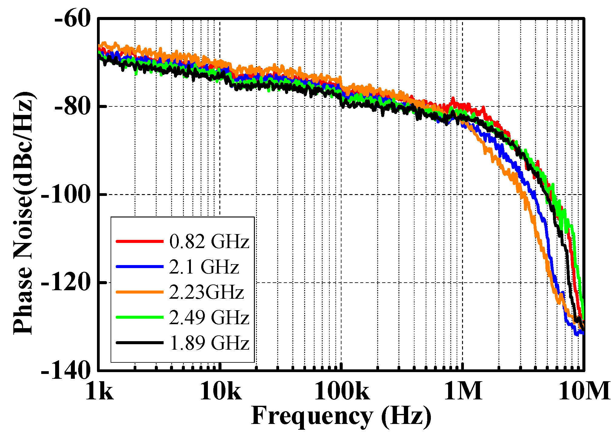
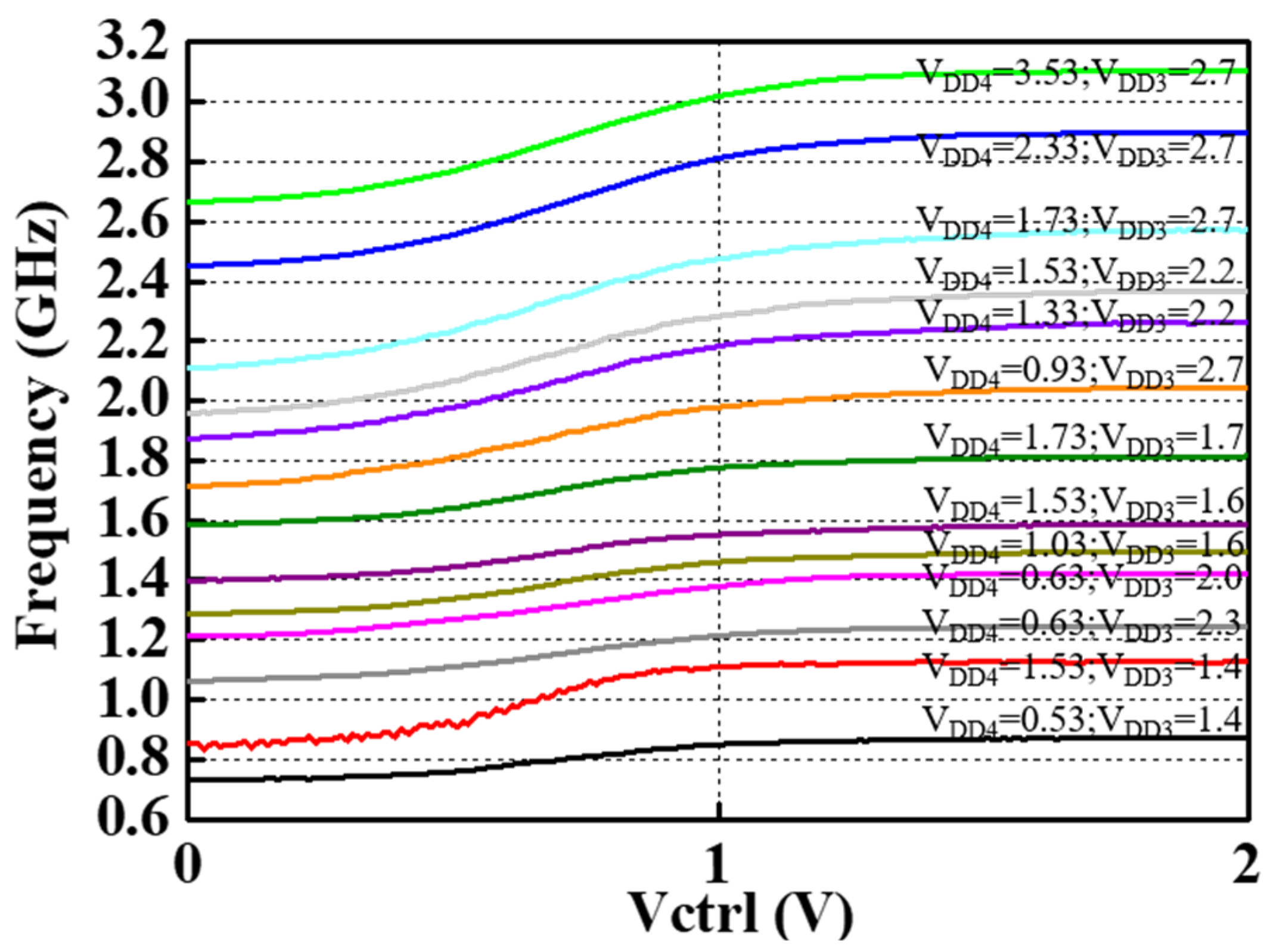
While operating at the supply voltage (VDD1) of 1.6 V and a VDD2 of 0.53 V, the VDD4 is tuned from 0.53 V to 3.53 V, and VDD3 is tuned from 1.4 to 2.7 V. In this condition, the VCO consumes around 6.8~10.1 mW, excluding the two output buffers. Figure 5 presents the measured frequency tuning range of the VCO. In general, the oscillation frequencies vary from 0.73 GHz to 3.1 GHz by adjusting the two control voltages (VDD4 and VDD3) of the active inductors and active resistors. It is also noted that the VCO consumes high DC power at high oscillation frequencies; namely, the DC power consumption of the line with VDD4 = 2.53 V and VDD3 = 2.7 V in Figure 5 is 10.1 mW. As shown in Figure 6, the measured output power is −15.5 dBm at 2.23 GHz, and the resolution bandwidth, video bandwidth, and span of the spectrum analyzer are 1 MHz, 10 MHz, and 100 MHz, respectively. Under a fixed 1 V of Vctrl and different VDD3,4 values as shown in Figure 5, the measured phase noise at different oscillating frequencies from 1 kHz to 10 MHz offset frequency are plotted in Figure 7. The measured phase noise from the 0.82 GHz, 2.23 GHz, and 2.49 GHz oscillating signals are −80.7, −84.5, and −83 dBc/Hz at a 1 MHz offset from the carriers, respectively. It is noted that the measured phase noise does not follow the conventional 1/f3 and 1/f2 decade, especially between the 1 kHz and 100 kHz offset frequencies. This poor phase noise below the 1 MHz offset frequency could have resulted from the coupling effect between the interconnections and noise from the active inductors. Besides flicker noise, the induced noise in the LC tank also includes shot noise and thermal noise. Therefore, the measured output spectrum in Figure 6 features some fluctuations. Table 2 summarizes the performances of the presented VCO and other previously reported CMOS VCOs based on the active-inductor topologies. As shown in the Table 2, the two 130 nm CMOS VCOs feature a lower PDC and a wider tuning range since the advanced process offers better trans-conductance (gm), which affects the active and tunable inductor directly. The common FOM and FOMT are also listed to fairly compare these VCOs [12]. It is observed that this work achieves lower DC power consumption and a wider tuning range of 123.8%, although its phase-noise performance is not good enough.
4. Conclusions
In this paper, a wide-tuning-range and low-power VCO using active inductors is designed, implemented, and verified in a standard 0.18 μm CMOS process. The active inductor incorporating a feedback active resistor not only achieves low power consumption but also increases the tuning range of the inductance. With a 6.7~10.1 mW DC consumption, the measured oscillating frequencies range from 0.73 GHz to 3.1 GHz and demonstrate a 123.8% tuning range. Moreover, the use of the differential active inductors reduces the chip size significantly, which allows the chip cost to be minimized. Compared with other CMOS VCOs based on active-inductor topologies, this work also features advantages in its low DC power consumption and superior wide-tuning range. The developed technique and VCO are applicable to the popular LTE 0.7 GHz and LTE 2.6 GHz bands.
Author Contributions
Conceptualization, S.W. and K.-C.H.; methodology, S.W.; software, K.-C.H.; validation, C.P. and S.W.; formal analysis, K.-C.H.; investigation, S.W. and K.-C.H.; resources, S.W.; data curation, K.-C.H.; writing—original draft preparation, C.P. and S.W.; writing—review and editing, C.P.; visualization, K.-C.H.; supervision, S.W.; project administration, C.P. and S.W.; funding acquisition, C.P. and S.W. All authors have read and agreed to the published version of the manuscript.
Funding
This work is supported by research funding under the Memorandum of Understanding of King Mongkut’s Institute of Technology Ladkrabang (grant number KREF156603), and the National Taipei University of Technology-King Mongkut’s Institute of Technology Ladkrabang Joint Research Program (NTUT-KMITL No. NTUT-KMITL-111-01).
Data Availability Statement
No new data were created or analyzed in this study. Data sharing is not applicable to this article.
Conflicts of Interest
The authors declare no conflicts of interest.
References
- Mukhopadhyay, R.; Park, Y.; Sen, P.; Srirattana, N.; Lee, J.; Lee, C.-H.; Nuttinck, S.; Joseph, A.; Cressler, J.D.; Laskar, J. Reconfigurable RFICs in Si-based technologies for a compact intelligent RF frontend. IEEE Trans. Microw. Theory Tech. 2005, 53, 81–93. [Google Scholar] [CrossRef]
- Dhamani, N.; Sepidband, P.; Entesari, K. A low phase noise wide-tuning range Class-F VCO based on a dual-mode resonator in 65nm CMOS. In Proceedings of the 2018 IEEE Radio and Wireless Symposium (RWS), Anaheim, CA, USA, 15–18 January 2018; pp. 277–280. [Google Scholar]
- Xu, S.; Zhang, W.; Shen, P.; Xie, H.; Jin, D.; Zhang, Y.; Yang, X.; Zhang, Z. A wide tuning range low Kvco and low phase noise VCO. In Proceedings of the 3rd International Conference on Integrated Circuits and Microsystems, Shanghai, China, 24–26 November 2018; pp. 47–50. [Google Scholar]
- Shu, R.; Subramanian, V.; Boeck, G.; Wu, J.; Lu, S. A wideband CMOS voltage-controlled oscillator with switched-capacitor array. In Proceedings of the German Microwave Conference Digest of Papers, Berlin, Germany, 15–17 March 2010; pp. 43–46. [Google Scholar]
- Yang, X.; Uchida, Y.; Xu, K.; Wang, W.; Yoshimasu, T. 2.4 GHz-band ultra-low-voltage Class-C LC-VCO IC in 65 nm CMOS Technology. In Proceedings of the 2013 Asia-Pacific Microwave Conference Proceedings (APMC), Seoul, Republic of Korea, 5–8 November 2013; pp. 325–327. [Google Scholar]
- Jeong, Y.J.; Kim, Y.M.; Chang, H.J. Low-power CMOS VCO with a low-current, high-Q active inductor. IET Microw. Antennas Propag. 2012, 6, 788–792. [Google Scholar] [CrossRef]
- Haddad, F.; Ghorbel, I.; Rahajandraibe, W. Multi-band inductor-less VCO for IoT applications. In Proceedings of the IEEE International Symposium on Circuits and Systems (ISCAS), Baltimore, MD, USA, 28–31 May 2017; pp. 1–4. [Google Scholar]
- Xu, J.; Saavedra, C.E.; Chen, G. An active inductor-based VCO with wide tuning range and high dc-to-RF power efficiency. IEEE Trans. Circuits Syst. II Express Briefs 2011, 58, 462–466. [Google Scholar] [CrossRef]
- Hammadi, A.B.; Mhiri, M.; Haddad, F.; Saad, S.; Besbes, K. An enhanced design of RF integrated differential active inductor. BioNanoScience 2016, 6, 185–192. [Google Scholar] [CrossRef]
- Zhang, Y.; Zhang, W.; Shen, P.; Xie, H.; Jin, D.; Xu, S.; Yang, X.; Zhang, Z. A novel LC VCO with high output power and low phase noise using differential active inductor. In Proceedings of the IEEE International Conference on Integrated Circuits and Microsystems (ICICM), Shanghai, China, 24–26 November 2018; pp. 90–93. [Google Scholar]
- Mehrabian, M.; Nabavi, A.; Rashidi, N. A 4-7GHz ultra wideband VCO with tunable active inductor. In Proceedings of the IEEE International Conference on Ultra-Wideband, Hannover, Germany, 10–12 September 2008; pp. 21–24. [Google Scholar]
- Wang, S.; Xiao, C.-Y. A 7/24-GHz CMOS VCO with High Band Ratio Using a Current-Source Switching Topology. IEEE Trans. Ultrason. Ferroelectr. Freq. Control 2016, 63, 790–795. [Google Scholar] [CrossRef] [PubMed]
Figure 1.
(a) The tunable active-resistor topology. (b) The resistance versus different sizes (channel width) with a Vtune of 2.2 V. (c) The resistance versus different tuning voltages of Vtune with a channel width of 4 μm.
Figure 1.
(a) The tunable active-resistor topology. (b) The resistance versus different sizes (channel width) with a Vtune of 2.2 V. (c) The resistance versus different tuning voltages of Vtune with a channel width of 4 μm.
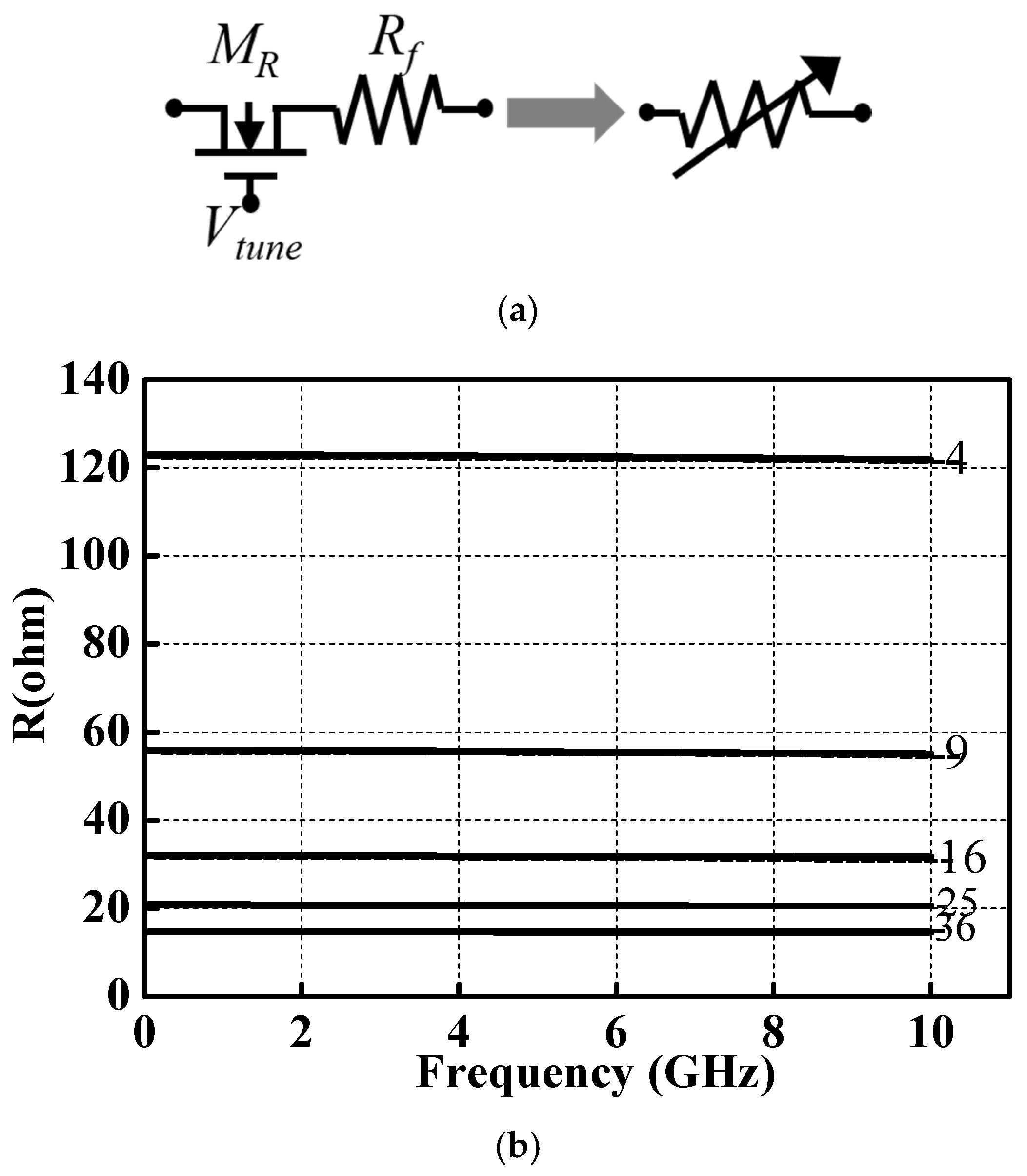
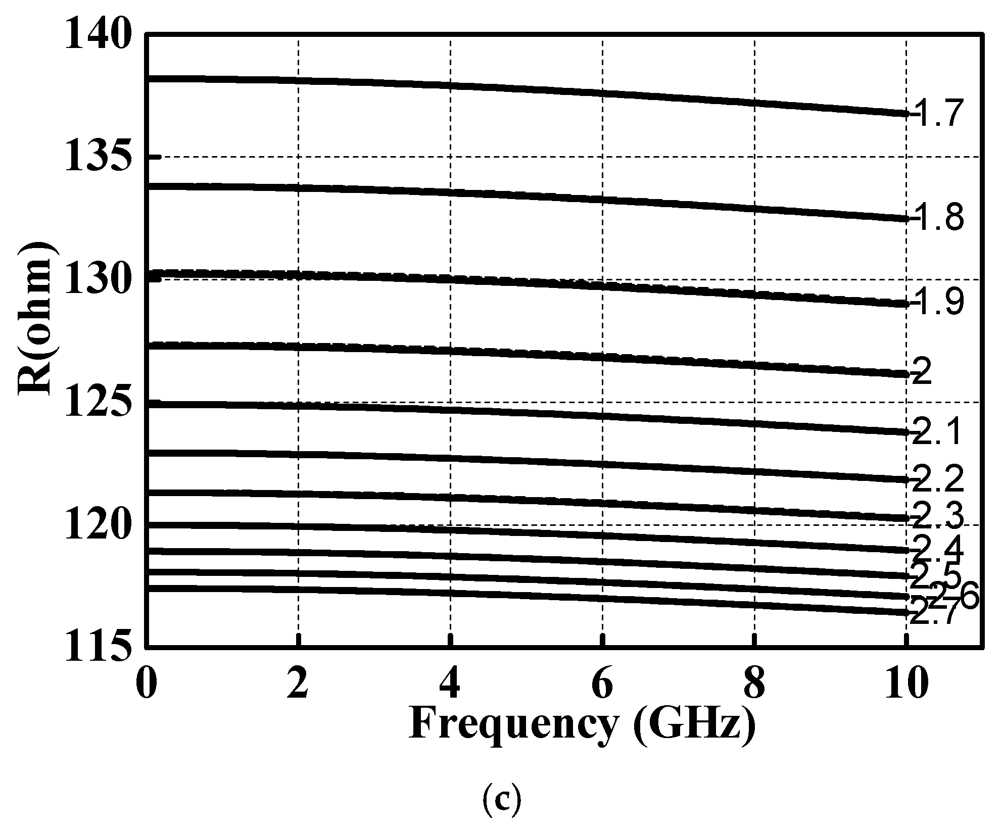
Figure 2.
(a) The proposed active inductor with a built-in active resistor. (b) Simulated inductances of the AI with a VDD1 of 1.6 V and a VDD2 of 0.53 V. (c) Simulated Q factors of the AI.
Figure 2.
(a) The proposed active inductor with a built-in active resistor. (b) Simulated inductances of the AI with a VDD1 of 1.6 V and a VDD2 of 0.53 V. (c) Simulated Q factors of the AI.

Figure 3.
Complete schematic of the proposed CMOS VCO.

Figure 4.
The photograph of the CMOS VCO.

Figure 5.
Measured oscillation frequencies versus control voltages.

Figure 6.
Measured 2.23 GHz oscillating frequency.
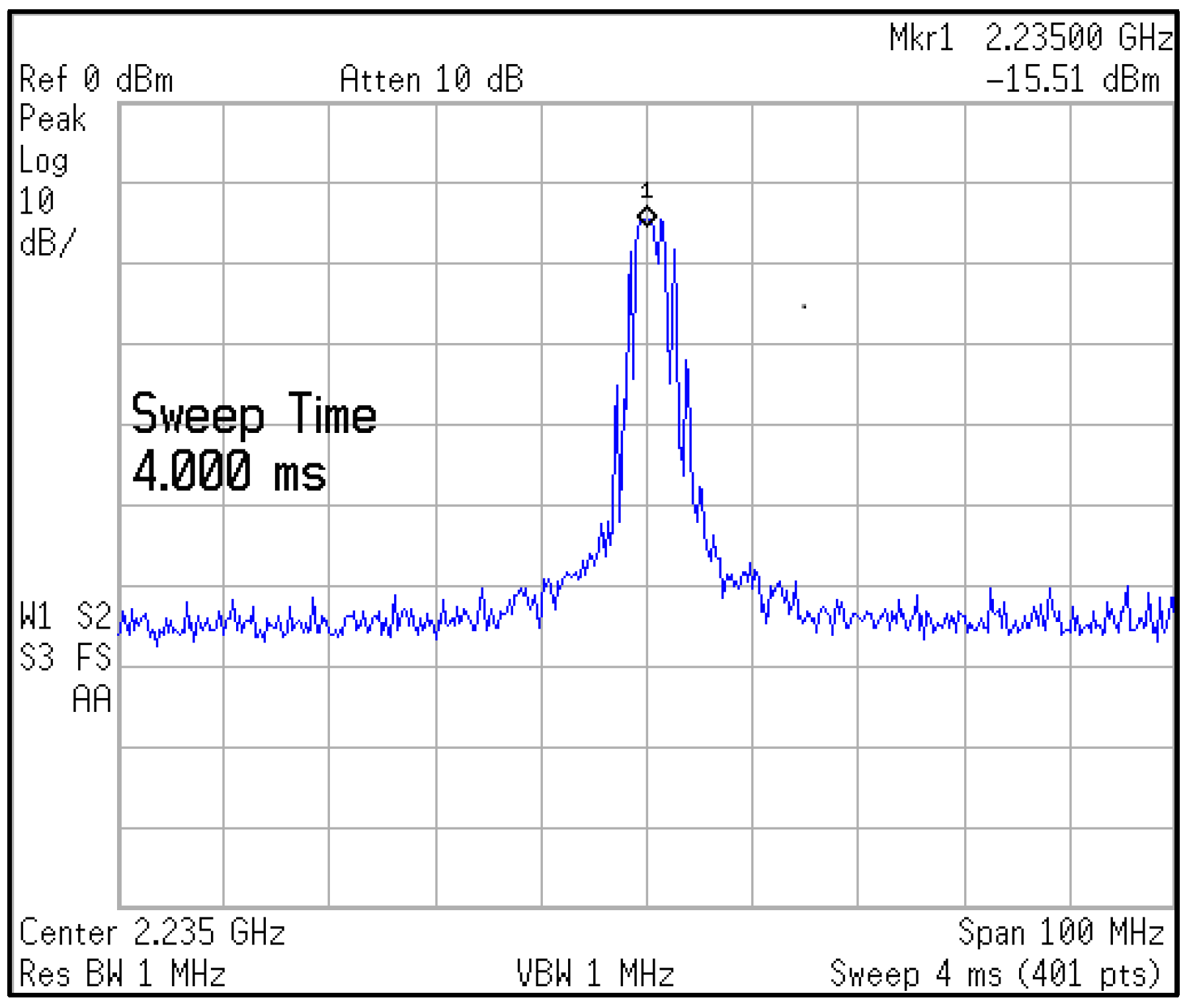
Figure 7.
Measured phase noise of different oscillating frequencies under a fixed 1 V of Vctrl and different VDD3,4, as shown in Figure 5.
Figure 7.
Measured phase noise of different oscillating frequencies under a fixed 1 V of Vctrl and different VDD3,4, as shown in Figure 5.

Table 1.
Design parameters of the proposed CMOS VCO.
| VDD1 = 1.6 V VDD2 = 0.53 V | VDD3 = 1.4~2.7 V | VDD4 = 0.53~3.53 V | Cvar = 373.9~493.7 fF |
| R1,2 = 900 Ω | R3,4 = 1.5 kΩ | C1,2 = 20.28 fF | C1,2 = 951.6 fF |
| M1,2 W/L (μm) = 16/0.18 | M3,6 W/L (μm) = 64/0.18 | M4,5 W/L (μm) = 4/0.18 | M7,10 W/L (μm) = 2/0.18 |
| M8,9 W/L (μm) = 60/0.18 | M11,12 W/L (μm) = 96/0.18 | M13,14 W/L (μm) = 400/0.18 | M15,16,17,18 W/L (μm) = 14/0.18 |
Table 2.
Comparison of CMOS VCOs based on an active-inductor topology.
| Reference | Process (nm) | Topology | fo (GHz) | Tuning Range (%) | PDC (mW) | Pout (dBm) | Phase Noise (dBc/Hz)@1MHz | FOM * (dBc/Hz) | FOMT * (dBc/Hz) | Area (mm2) |
|---|---|---|---|---|---|---|---|---|---|---|
| [6] IET MAP’12 | 180 | Active L | 1.13~2.67 | 81 | 2.2~13 | −14.3 | −82.8~−92.2 | −144.2 | −162.4 | 0.03 |
| [7] ISCAS’17 | 130 | Active L | 1.28~2.6 | 68 | 3.8~4 | N.A. | −81~−87 | −143.8 | −160.5 | 0.0031 |
| [8] TCAS-II’11 | 130 | Active L | 0.83~3.72 | 127 | 8~13 | −0.9 | −104~−109 | −163.4 | −185.5 | 0.108 |
| [10] ** ICICM’18 | 180 | Active and Differential L | 1.13~2.71 | 82.3 | 13.6 | −4.2 | −101~−105 | −157.3 | −175.6 | N.A |
| [11] ** ICUWB’08 | 180 | Active L + Parallel R | 3.8~7.4 | 64.2 | 29.1 | N.A | −75~−92 | −143.8 | −159.9 | N.A |
| This work | 180 | Active L + Series R | 0.73~3.1 | 123.8 | 6.8~10.1 | −15.5 | −80.7~−84.5 | −139 | −160.8 | 0.046 |
* The best values. ** Simulation results.
Disclaimer/Publisher’s Note: The statements, opinions and data contained in all publications are solely those of the individual author(s) and contributor(s) and not of MDPI and/or the editor(s). MDPI and/or the editor(s) disclaim responsibility for any injury to people or property resulting from any ideas, methods, instructions or products referred to in the content. |
© 2024 by the authors. Licensee MDPI, Basel, Switzerland. This article is an open access article distributed under the terms and conditions of the Creative Commons Attribution (CC BY) license (https://creativecommons.org/licenses/by/4.0/).
Share and Cite
MDPI and ACS Style
Pakasiri, C.; Hsu, K.-C.; Wang, S. A Compact 0.73~3.1 GHz CMOS VCO Based on Active-Inductor and Active-Resistor Topology. J. Low Power Electron. Appl. 2024, 14, 18. https://doi.org/10.3390/jlpea14020018
AMA Style
Pakasiri C, Hsu K-C, Wang S. A Compact 0.73~3.1 GHz CMOS VCO Based on Active-Inductor and Active-Resistor Topology. Journal of Low Power Electronics and Applications. 2024; 14(2):18. https://doi.org/10.3390/jlpea14020018
Chicago/Turabian StylePakasiri, Chatrpol, Ke-Chung Hsu, and Sen Wang. 2024. "A Compact 0.73~3.1 GHz CMOS VCO Based on Active-Inductor and Active-Resistor Topology" Journal of Low Power Electronics and Applications 14, no. 2: 18. https://doi.org/10.3390/jlpea14020018
Note that from the first issue of 2016, this journal uses article numbers instead of page numbers. See further details here.