1. Introduction
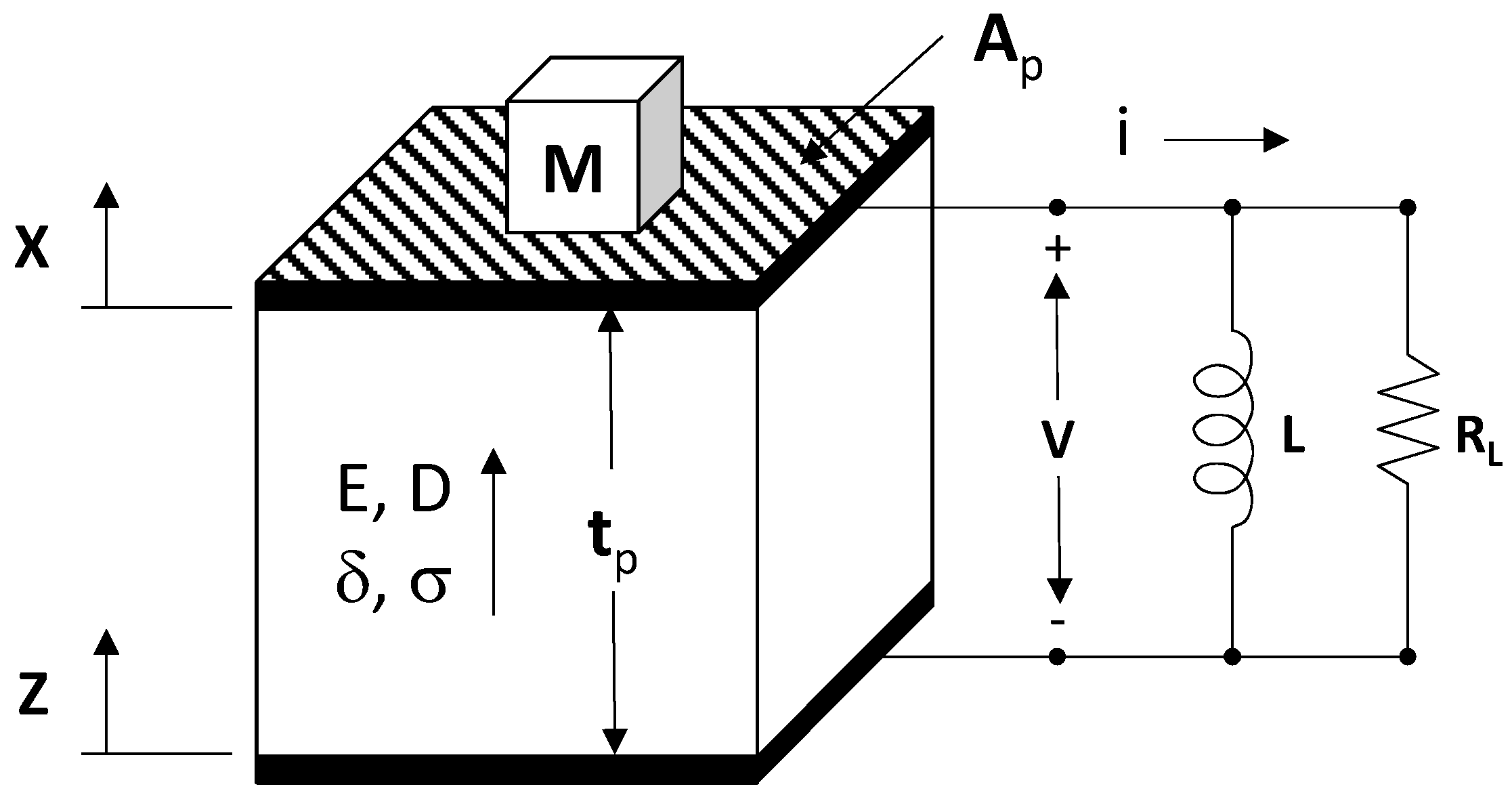
Figure 1 shows a schematic of a Piezoelectric (PZ) Energy Harvesting Device (EHD) that is the subject of this research. This structure is referred to as a cantilever structure, and is used to amplify the amplitude of the source vibration [
1]. Previous work has shown that maximum output power is achieved when the cantilever has a high Q resonance at the frequency of the source vibration. However, the frequency of the source vibration is not usually matched to the resonant frequency of the EHD. The source vibration may vary with time. This paper addresses the problem of electronically tuning the PZ EHD to achieve maximum power in situations where the source vibration is not a stable frequency matched to the mechanical resonant frequency of the EHD.
Figure 1.
Schematic of a Piezo-Electric (PZ) Energy Harvesting Device (EHD) based on the Cantilever Beam structure.
Figure 1.
Schematic of a Piezo-Electric (PZ) Energy Harvesting Device (EHD) based on the Cantilever Beam structure.
In the interest of simplicity, we will analyze the structure in
Figure 2. The results achieved through analysis of this structure can be generalized to the cantilever structure through the addition of geometrical constants.
Figure 2.
Schematic of the simplified EHD that is analyzed in this paper. A
p is the area of the PZ capacitor, and t
p is the thickness. Z is the complex amplitude of the source vibration, and X is the complex amplitude of the mechanical displacement of the mass M. This simplified model illustrates the concepts of electronic tuning that apply to the cantilever structure of
Figure 1.
This paper describes three concepts for electrically tuning of PZ EHDs.
Use of voltage amplitude to tune the mechanical stiffness of the EHD;
Coupling of the mechanical resonator to an electrical RLC tank circuit;
Bias-Flip (BF) technique to emulate the large tunable inductor that is required for the RLC tank circuit.
These three concepts were introduced in summary form in [
2]. In the succeeding sections of this paper, these concepts will be presented in more detail.
Section 6 shows that BF can be used to effectively optimize the power output from a PZ EHD. In this paper, we have changed some of the notation that we used in [
2], in order to conform to generally accepted usage.
In this paper, we will analyze the PZ EHD. However, many of the results and conclusions are equally applicable to electromagnetic and electrostatic EHDs. Cammarano
et al. [
3] have described concepts very similar to #1 and #2 above in the context of electro-magnetic EHDs.
2. Frequency Tuning by Voltage
The material equations for PZ material can be written as follows [
1].
The parameters are defined below.
δ = mechanical strain (displacement/length)
σ = mechanical stress (force/area)
Y = Young’s Modulus (force/area)
d = piezo-electric (PZ) coefficient (m/volt)
![Jlpea 03 00194 i022]()
PZ coupling constant
E = electric field (volt/m)
D = electrical displacement (coulomb/m2)
ε = dielectric constant (coul/volt-m)
km = mechanical (short-circuit) spring constant
![Jlpea 03 00194 i023]()
mechanical (short-circuit) resonant frequency
![Jlpea 03 00194 i024]()
electrical (
σ = 0) capacitance
![Jlpea 03 00194 i025]()
motion constrained (
δ = 0) capacitance.
L = inductance
![Jlpea 03 00194 i026]()
motion constrained resonant frequency
η = mechanical damping factor (force/velocity)
![Jlpea 03 00194 i027]()
mechanical Q-factor
![Jlpea 03 00194 i028]()
load conductance
![Jlpea 03 00194 i029]()
normalized load conductance
![Jlpea 03 00194 i030]()
internal conductance
![Jlpea 03 00194 i031]()
normalized internal conductance
Refer to the device of
Figure 2. When the output is shorted, E = 0, and the mechanical stiffness is given by Young’s modulus,
![Jlpea 03 00194 i032]()
. The short-circuit, resonance frequency is given by
![Jlpea 03 00194 i033]()
. However, when the output is in the open circuit condition, D = 0; the open-circuit stiffness is given by
![Jlpea 03 00194 i034]()
, where
ρ is the dimensionless PZ coupling constant, defined in
Table 1. From this, it can be shown that the open-circuit and short-circuit resonant frequencies
ωoc and
ωm are related by the equation
![Jlpea 03 00194 i035]()
. This relationship is well-known, and has been used to experimentally determine the coupling constant ρ [
1].
Similarly, we define the electrical capacitance
![Jlpea 03 00194 i036]()
for the case when there is no stress (
σ = 0); and we define the motion constrained capacitance
![Jlpea 03 00194 i037]()
for the case when δ = 0.
The equations for the PZ EHD shown in
Figure 2 are given below
These equations can be solved for V(ω) and X(ω) as shown below.
When the source vibration frequency ω equals the mechanical resonant frequency ωm, Equation (5) for output voltage reduces to a familiar form.
where
![Jlpea 03 00194 i038]()
and
![Jlpea 03 00194 i039]()
.
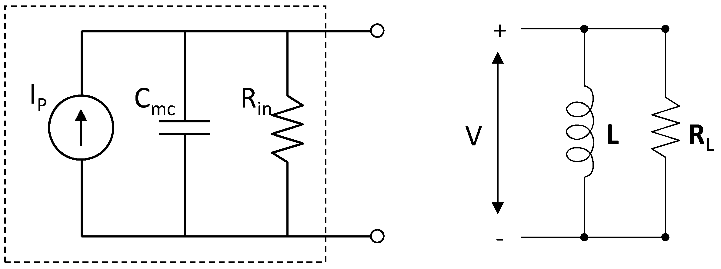
This results in the familiar circuit model for the PZ EHD, shown at the left of
Figure 3.
Figure 3.
The circuit within the dashed box is the equivalent circuit that applies to a PZ EHD when ω=ωm. At this frequency, the PZ current Ip is independent of the load. For ω ≠ ωm this equivalent circuit does not accurately model device behavior, because the PZ current Ip changes as the load changes. The circuit at the right includes an inductor to cancel the capacitive reactance of the EHD.
If a purely resistive load is connected to the EHD, the device capacitance Cmc degrades output power. As a result, an inductor (or an effective inductor) is added to the output circuit for the purpose of cancelling the capacitive admittance and achieving maximum average power to the load.
In succeeding sections, simulations of voltage and output power are shown as a function of frequency. In [
2] simulations were shown for
ρ = 0.2;
Qm = 50; and
![Jlpea 03 00194 i040]()
. Throughout this paper, simulations are shown for
ρ = 0.05;
Qm = 20; and
![Jlpea 03 00194 i041]()
. These values are more representative of today’s commercial devices.
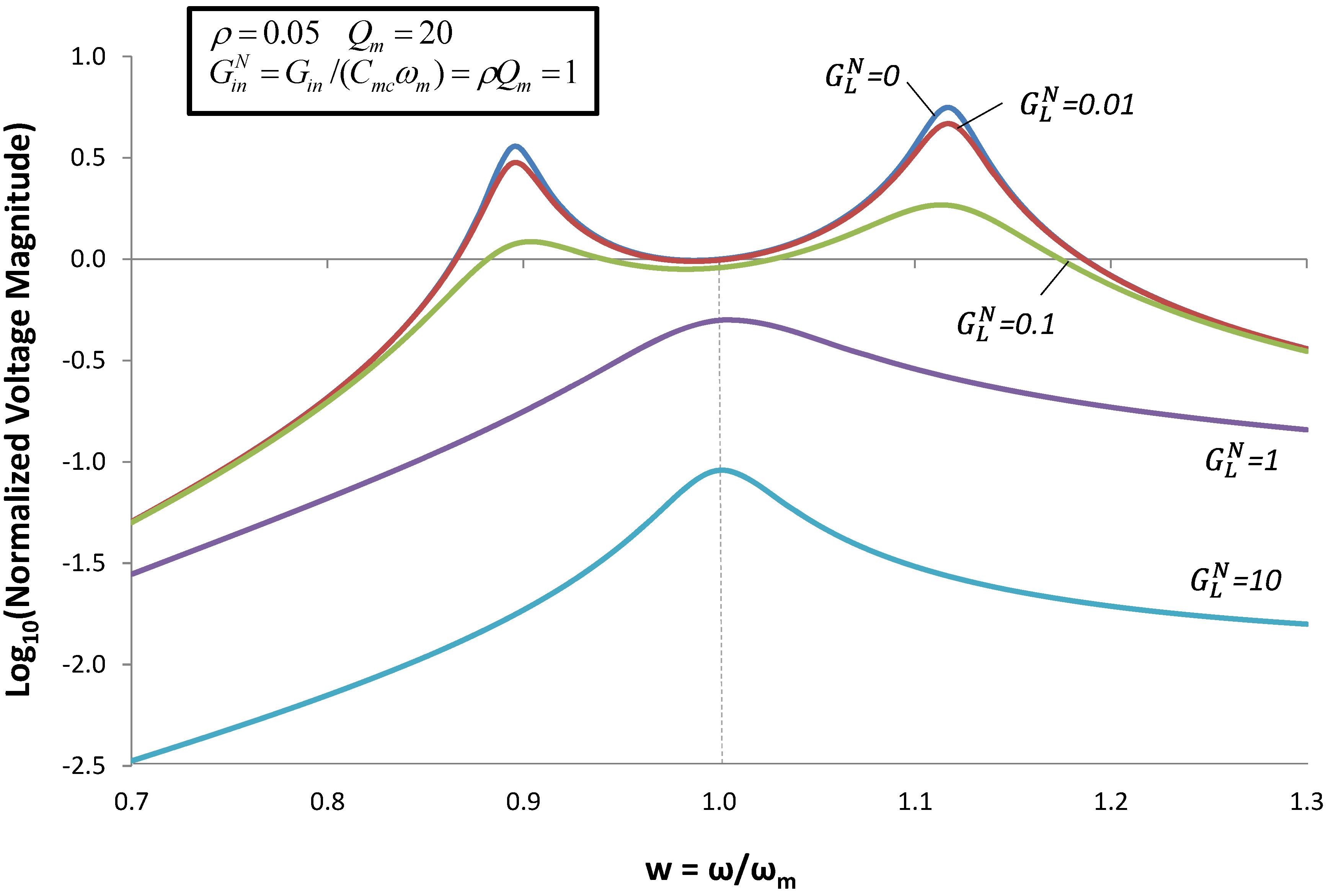
Figure 4.
Voltage magnitude for the case of no inductor. Voltage is normalized to Z / d, the open-circuit voltage at w = 1.
Figure 4.
Voltage magnitude for the case of no inductor. Voltage is normalized to Z / d, the open-circuit voltage at w = 1.
Figure 4 shows the magnitude of the output voltage as a function of frequency, calculated using Equation (5), for the case of no inductor (
ωmc = 0). On the vertical axis, voltage is normalized to the maximum open-circuit voltage at the mechanical resonant frequency
![Jlpea 03 00194 i042]()
. Frequency, on the horizontal axis, is normalized to
ωm. For
![Jlpea 03 00194 i043]()
,
Figure 4 confirms the predictions of Equation (7). For
![Jlpea 03 00194 i044]()
, the normalized voltage magnitude is 0.707; and for
![Jlpea 03 00194 i045]()
, the normalized voltage magnitude is 0.447. However, for
w ≠ 1,
Figure 4 shows interesting behavior, especially for
![Jlpea 03 00194 i046]()
. For
![Jlpea 03 00194 i044]()
, the voltage shows a resonance at
![Jlpea 03 00194 i047]()
.
Figure 4 shows that, for large
![Jlpea 03 00194 i048]()
, the voltage peaks at the mechanical or short-circuit resonance frequency
ωm. However, for small
![Jlpea 03 00194 i048]()
, the device characteristics change. When
![Jlpea 03 00194 i044]()
, the peak voltage occurs at
![Jlpea 03 00194 i047]()
. This can be understood as follows. For large
![Jlpea 03 00194 i048]()
, the electric field is effectively shorted. As
![Jlpea 03 00194 i048]()
decreases, the electric field in the EHD increases, and alters the effective spring constant of the cantilever beam.
It is tempting to assume from the above that frequency tuning is possible only in the narrow range
![Jlpea 03 00194 i049]()
[
4]. However, as we will see below, the addition of a resonant electrical circuit allows the voltage to swing below zero and above
Voc, thereby enabling a wider tuning range.
3. Coupled Oscillators
In the simulations in the previous section, we did not attempt to cancel the reactive admittance of the PZ capacitor, and we observed the degradation in output voltage. Since
![Jlpea 03 00194 i050]()
in the simulations above, the degradation is not large. However, in some cases, the PZ EHD has a large capacitance, which can substantially degrade output power at
ω =
ωm. In
Figure 5, we simulate Equation (5) for the case
ωmc =
ωm. This is equivalent to adding an inductor that cancels the reactive admittance of the capacitor at
ω =
ωm. The inductor performs as expected at
ω =
ωm. The output voltage equals
![Jlpea 03 00194 i051]()
. Moreover, for large
![Jlpea 03 00194 i048]()
, the output voltage continues to show a resonant peak at
ω =
ωm; and the voltage falls away sharply away from
ω =
ωm.
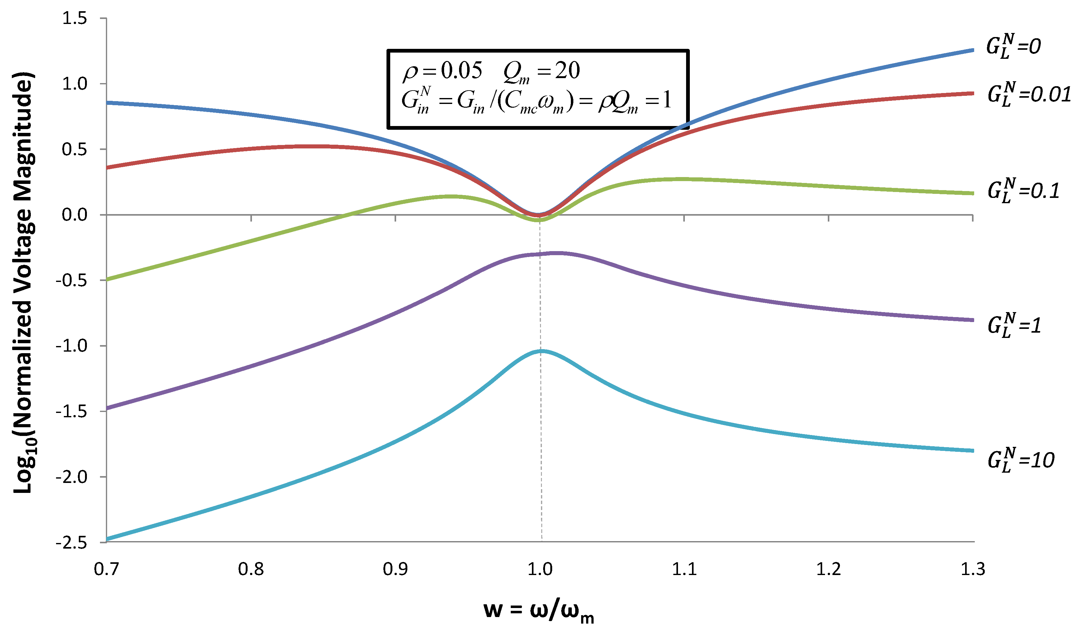
However, for
ω ≠
ωm,
Figure 5 shows a surprising result when
![Jlpea 03 00194 i048]()
is small. Two peaks occur at
![Jlpea 03 00194 i052]()
and
![Jlpea 03 00194 i053]()
. These resonances result from the poles in the denominator of Equation (5) when
![Jlpea 03 00194 i044]()
.
Solution to the pole-splitting equation above, for the case
ωmc =
ωm and
ρ = 0.05 gives the values of
w+ and
w− above. Note that, when
ωmc = 0 (case of no inductor), the solutions of Equation (9) are
w− = 0 and
![Jlpea 03 00194 i054]()
. Pole splitting, which describes coupled modes of the mechanical and electrical resonators, occurs only for small
![Jlpea 03 00194 i048]()
. When
![Jlpea 03 00194 i048]()
is large, the electric field in the PZ material is screened, and coupling is suppressed.
Figure 5.
Voltage magnitude for the case when an inductor of value
![Jlpea 03 00194 i055]()
is added to the circuit. Voltage is normalized as in
Figure 4.
Figure 5.
Voltage magnitude for the case when an inductor of value
![Jlpea 03 00194 i055]()
is added to the circuit. Voltage is normalized as in
Figure 4.
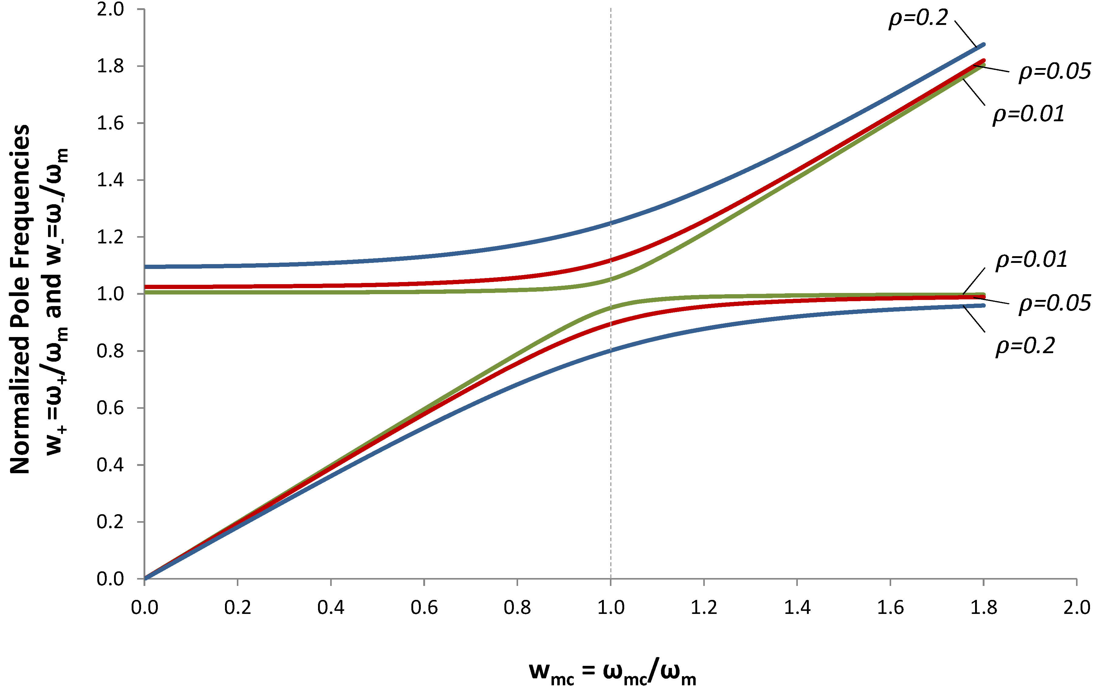
Figure 6.
Roots of the Pole-splitting Equation (9). The normalized pole frequencies
![Jlpea 03 00194 i056]()
and
![Jlpea 03 00194 i057]()
are plotted
vs.
![Jlpea 03 00194 i058]()
.
Figure 6.
Roots of the Pole-splitting Equation (9). The normalized pole frequencies
![Jlpea 03 00194 i056]()
and
![Jlpea 03 00194 i057]()
are plotted
vs.
![Jlpea 03 00194 i058]()
.
The roots of the pole-splitting equation are shown in
Figure 6 for several values of coupling constant
ρ. In
Figure 5, we selected
ωmc =
ωm, in order to optimize output power at
ω =
ωm. But, we discovered that, if we increased the load resistance, we could also optimize output voltage at
w+ and
w−. (We will show in the next section that output power is also optimized at these frequencies). This analysis suggests that we can tune the EHD resonant frequency by varying
ωmc.
We can gain further insight into the pole-splitting by returning to Equations (5) and (6). For small
![Jlpea 03 00194 i048]()
, the following relationship holds between
X(
ω) and
V(
ω).
Using Equation (10) the force of the spring can be written as
The above equation shows that, by tuning L, we can vary
ωmc and vary the effective spring constant. When
ω <
ωmc,
V(
ω) has a phase of 180° relative to
X(
ω); and the voltage reduces the effective spring constant. When
ω >
ωmc,
V(
ω) has a phase of 0° relative to
X(
ω); and the voltage increases the effective spring constant. When
ω =
ωmc, the magnitude of
X(
ω) is zero. If we adjust
ωmc such that the corresponding root of Equation (9) equals the source vibration frequency, then Equation (11) reduces to
Equation (12) shows that the effective spring constant can be tuned over a wide range.
It is also somewhat surprising that the peak voltages at
ω− and
ω+ are 3.5× to 5.5× higher than
![Jlpea 03 00194 i051]()
. The simulations in this paper assume that the source magnitude
Z is held constant as the frequency changes. As a result, the input acceleration increases in proportion to
ω2, and
![Jlpea 03 00194 i059]()
. The important result is that the peak voltages away from resonance can be somewhat higher than
![Jlpea 03 00194 i051]()
, and the higher voltage enables frequency tuning.
4. Optimizing Output Power
In the previous section, we showed that voltage can be made to peak at frequencies
ω− and
ω+, which are different from
ωm.
Figure 7 shows that power is also maximized at these frequencies. The curve for
![Jlpea 03 00194 i060]()
indicates that output power peaks at
ω =
ωm, at the power
![Jlpea 03 00194 i061]()
given by Equation (8). The curve for
![Jlpea 03 00194 i063]()
shows a peak at
ω =
ωm at a degraded power level. The curve for
![Jlpea 03 00194 i062]()
shows two peaks at
ω− and
ω+ that have output power comparable to
![Jlpea 03 00194 i061]()
. When
![Jlpea 03 00194 i048]()
is further reduced to
![Jlpea 03 00194 i064]()
, the output power at
ω− and
ω+ decreases.
Figure 7.
Normalized average output power for the case when an inductor of value
![Jlpea 03 00194 i091]()
is added to the circuit. Average power is normalized by
![Jlpea 03 00194 i061]()
Equation (8).
Figure 7.
Normalized average output power for the case when an inductor of value
![Jlpea 03 00194 i091]()
is added to the circuit. Average power is normalized by
![Jlpea 03 00194 i061]()
Equation (8).
Figure 7 suggests that output power can be optimized at frequencies different from
ωm by adjusting the external inductor (or effective inductor). Equation (5) provides a general expression for
V(
ω). Varying the parameter
![Jlpea 03 00194 i065]()
in Equation (5) is equivalent to varying the inductor. Maximizing power with respect to
ωmc gives the expression
When we use Equation (13) to determine the value of
ωmc that optimizes power at each frequency, the resulting voltage and power are shown in
Figure 8,
Figure 9.
Equation (13) suggests that we need two strategies for optimizing power, depending on the source frequency
ω. For frequencies near
ωm, (Region 2), Equation (13) reduces to
Note that, when
ω =
ωm, Equation (14) reduces further to
ωmc =
ωm, which is equivalent to matching the capacitive admittance (refer to
Figure 3). When
ω is above or below
ωm (Regions 1 and 3), Equation (13) reduces to the pole-splitting Equation (9). Far from
ωm, output power is maximized at the pole frequencies [roots of Equation (9)]. However, as
ω approaches
ωm, interaction between the poles shifts the max-power frequency [given by Equation (13)] slightly away from the pole frequency.
Figure 8.
Normalized voltage magnitude for the case when the reactive admittance is optimized to give maximum output power using Equation (13). Plots of Voltage
vs. frequency are given for different values of normalized load conductance
![Jlpea 03 00194 i048]()
. These plots can be thought of as envelopes of curves such as
Figure 5 for different values of
ωmc.
Figure 9.
Normalized average power for the case when the reactive admittance is optimized to give maximum output power using Equation (13). Plots of power
vs. frequency are given for different values of normalized load conductance
![Jlpea 03 00194 i048]()
. Power increases with increasing
ω because source acceleration increases, thereby increasing input power.
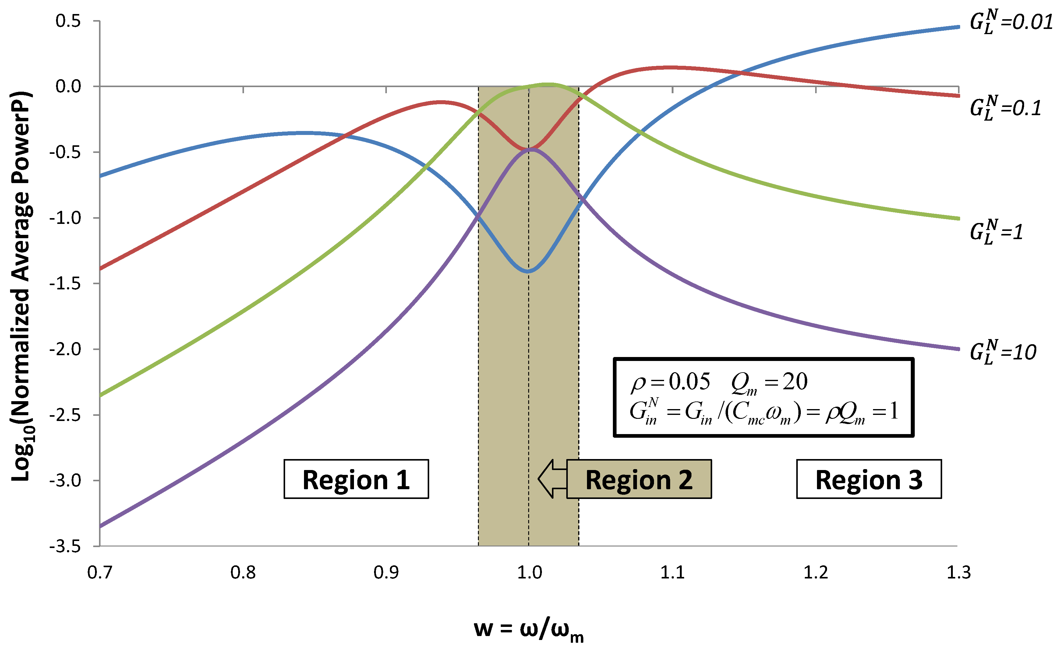
Within the region
![Jlpea 03 00194 i066]()
around the mechanical resonant frequency (Region 2), output power can be optimized by using (14) for reactive admittance and
![Jlpea 03 00194 i067]()
. In Regions 1 and 3, power is optimized by using the pole splitting Equation (9) for reactive admittance and
![Jlpea 03 00194 i068]()
. For the parameters used in this example (
Qm = 20), Δ
w ≈ 0.025.
Cammarano
et al. [
3] have derived an equation very similar to Equation (13): Equation (8) in [
3]. They observe that the power conditioning system at the output of the EHD can be used to synthesize the complex load impedance required by Equation (13), and they comment on the challenge of reducing the power of such systems. Chang
et al. [
5] have implemented a switch-mode power conditioning system to the output of a PZ EHD, and have demonstrated the ability to harvest energy from two sources simultaneously:
ω =
ωm and
ω = 1.2
ωm.
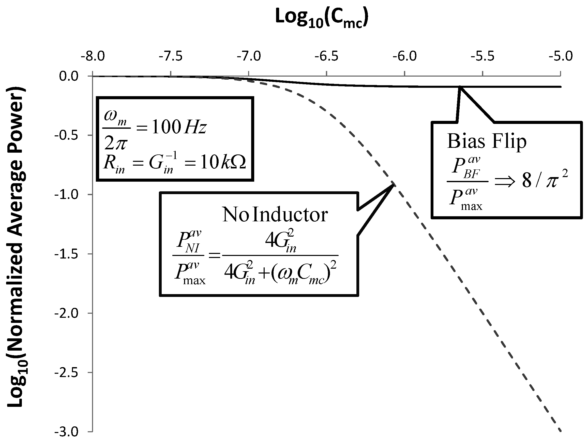
5. Bias-Flip Technique
For a typical, discrete EHD,
Cmc ≈ 100
nF, and the inductor required to match this reactance at 100 Hz is impractically large:
L ≈ 25
H. However, it has been shown that the Bias-Flip technique can be used to synthesize a reactive impedance for effective impedance matching [
6,
7]. This technique is suitable to ULP miniaturization. It utilizes a very small inductor together with ULP microelectronics to emulate an inductor that is large and tunable. The BF technique has been shown to be effective in maximizing the output power of PZ EHDs at
ω =
ωm [
7]. In this section, we will describe the Bias-Flip technique in the context of the equivalent circuit of
Figure 3 describing a PZ EHD operating at the mechanical resonance frequency.
Figure 10.
Operation of a Bias Flip (BF) Inductor. (a) A small inductor is connected to the output through ideal switches; (b) When the switchers are closed, the LC tank circuit begins to oscillate, when the switches are opened, half a period later, the sign of the voltage has been adiabatically “flipped”; (c) To achieve maximum power to the load, the bias is flipped when Ip changes sign; (d) The resulting voltage waveform is “in-phase” with the current.
The BF technique is illustrated in
Figure 10. In the BF circuit, the large inductor is replaced by a small inductor, connected by MOS switches. When the switches are closed, a high frequency tank circuit is formed. After ½ period of oscillation of this tank circuit, the switches are opened, and the voltage on the capacitor has “flipped” adiabatically from +V to −V. In this paper, the switches are assumed to be ideal and lossless.
Refer to
Figure 3. When an ideal inductor is used together with a matched resistive load
RL =
Rin, the maximum average output power is given by
![Jlpea 03 00194 i069]()
. [See Equation (8)] In
Figure 11, we show how effective the ideal Bias-Flip circuit is in achieving maximum power.
Figure 11.
Normalized Average Power delivered to the load at
ω =
ωm. The equivalent circuit of Fig 3 is used with
RL =
Rin. The dashed line shows the case of no inductor. The solid line shows the improvement in output power that is achievable using the Bias-Flip inductor. Both curves are normalized to the average power obtained using an ideal tuned inductor
![Jlpea 03 00194 i069]()
.
In the worst case of very large
Cmc, the output power is degraded by several orders of magnitude, when no inductor is used. However, the Bias-Flip approach delivers power
![Jlpea 03 00194 i070]()
, which is 8 /
π2 = 81% of the max power obtained using an ideal inductor. This illustrates the effectiveness of Bias-Flip circuits to achieve high output power when
Cmc is large [
7].
So far in this paper, we have discussed the case in which AC power is delivered to a resistive load. We have done this because the analysis can be performed in closed form. However, in many energy harvesting applications, it is necessary to rectify the AC power and store it in a battery or super-capacitor. The Bias-Flip technique is especially applicable to this case, as shown in [
7].
The rectification circuit analyzed in [
7] is shown in
Figure 12. For simplicity, we assumed that the EHD is operating at the mechanical resonance frequency, and we use the equivalent circuit of
Figure 3. The output AC voltage
v(
t) is rectified in the diode bridge and stored on the capacitor
CRECT that is maintained at voltage
VRECT by the Energy Management Circuit. The analysis below assumes ideal diodes.
Figure 12.
Circuit to rectify and store the AC power being generated by the EHD. It is assumed that the EHD is operating at the mechanical resonance frequency.
Figure 12.
Circuit to rectify and store the AC power being generated by the EHD. It is assumed that the EHD is operating at the mechanical resonance frequency.
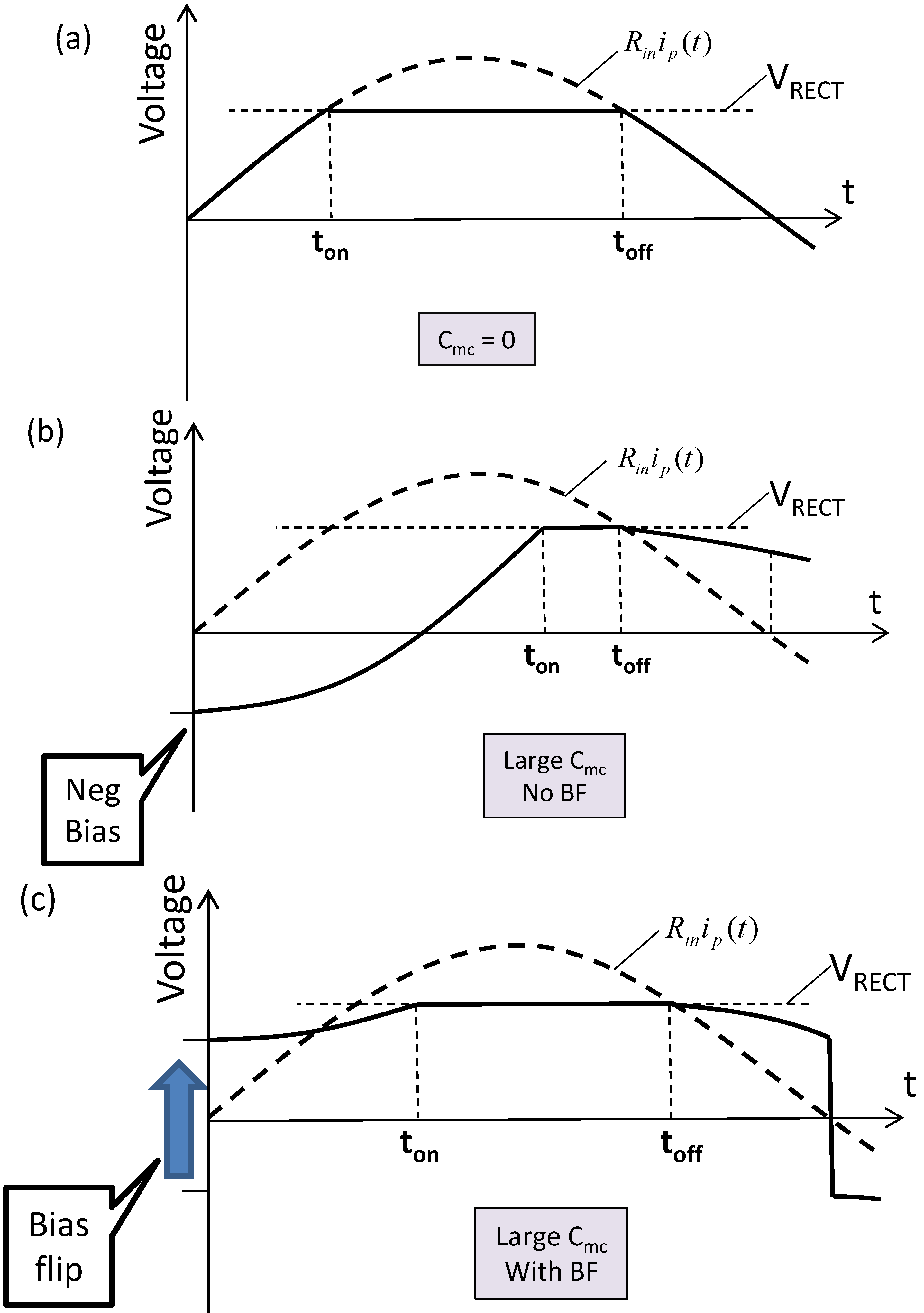
Operation of the Bias-Flip rectifier is described with reference to
Figure 13.
Figure 13.
(
a) Voltage waveform
v(
t) in
Figure 12 for the case
Cmc = 0; in this case, the Bias-Flip circuit is not required; (
b) Voltage waveform for the case of large
Cmc without Bias-Flip compensation; when the current becomes positive, there is a large negative voltage on the capacitor
Cmc, this must be discharged before the voltage can swing positive; (
c) When the current becomes positive, the polarity of the voltage
v(
t) is “flipped”. This reduces the time to diode turn-on and increases power transferred to
CRECT.
When the capacitance is zero, as shown in
Figure 13a, Bias-Flip is not required.
![Jlpea 03 00194 i071]()
until
t =
ton; at which time,
v(
t) becomes clamped at
VRECT. Between
ton and
toff power is supplied to the storage unit. At
t =
toff, the diodes turn off, and
v(
t) returns to zero following the curve
![Jlpea 03 00194 i071]()
. The presence of non-zero
Cmc degrades transferred power:
Figure 13b. When the current turns positive, there is a negative bias on
Cmc that must be discharged before the voltage can swing positive. This delays diode turn-on, and forces a reduction in
VRECT, both of which degrade transferred power. This degradation can be corrected by adiabatically flipping the bias on
Cmc when the current changes sign, as illustrated in
Figure 13c.
Figure 14.
Power transferred to the storage capacitor
CRECT as a function of
VRECT for different values of
Cmc. Power is normalized to
![Jlpea 03 00194 i061]()
(see Equation (8)). The curve for
Cmc = 0 is negligibly different from the curve for
Cmc = 10
nF, and is not shown. For the case of no capacitor, the max power transfer of 0.92 occurs at
![Jlpea 03 00194 i072]()
.
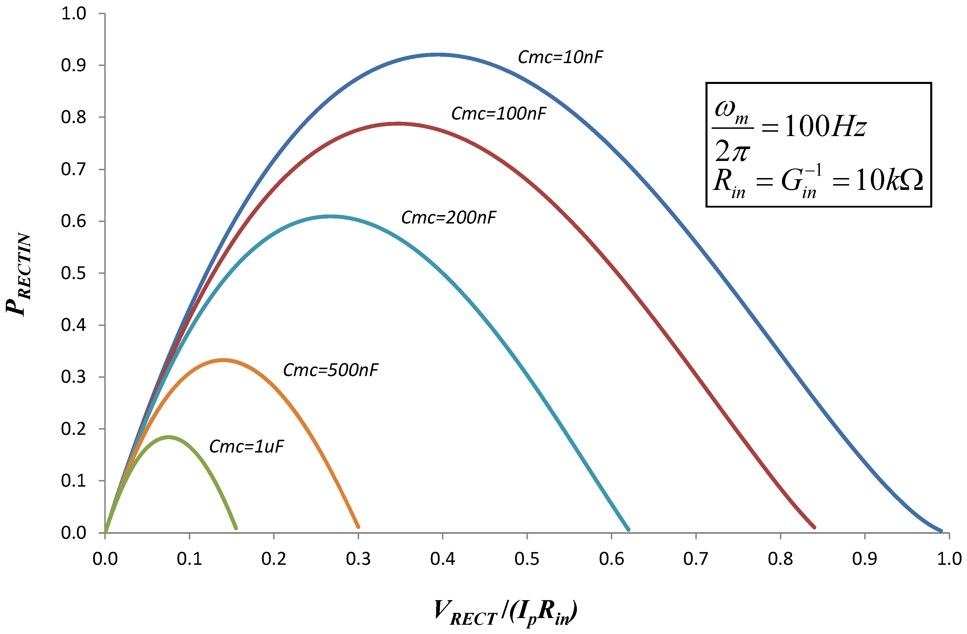
The energy transferred per cycle depends on
VRECT. When
VRECT is low, the power transfer interval
toff −
ton is long, but the power is low. When
VRECT is high, the power transfer is high, but the transfer interval is short. In fact, for
VRECT above a maximum value the diodes do not turn on, and no power is transferred.
Figure 14 shows the power transfer as a function of
VRECT, for various values of
Cmc. This simulation is made using the values
![Jlpea 03 00194 i073]()
and
![Jlpea 03 00194 i074]()
.
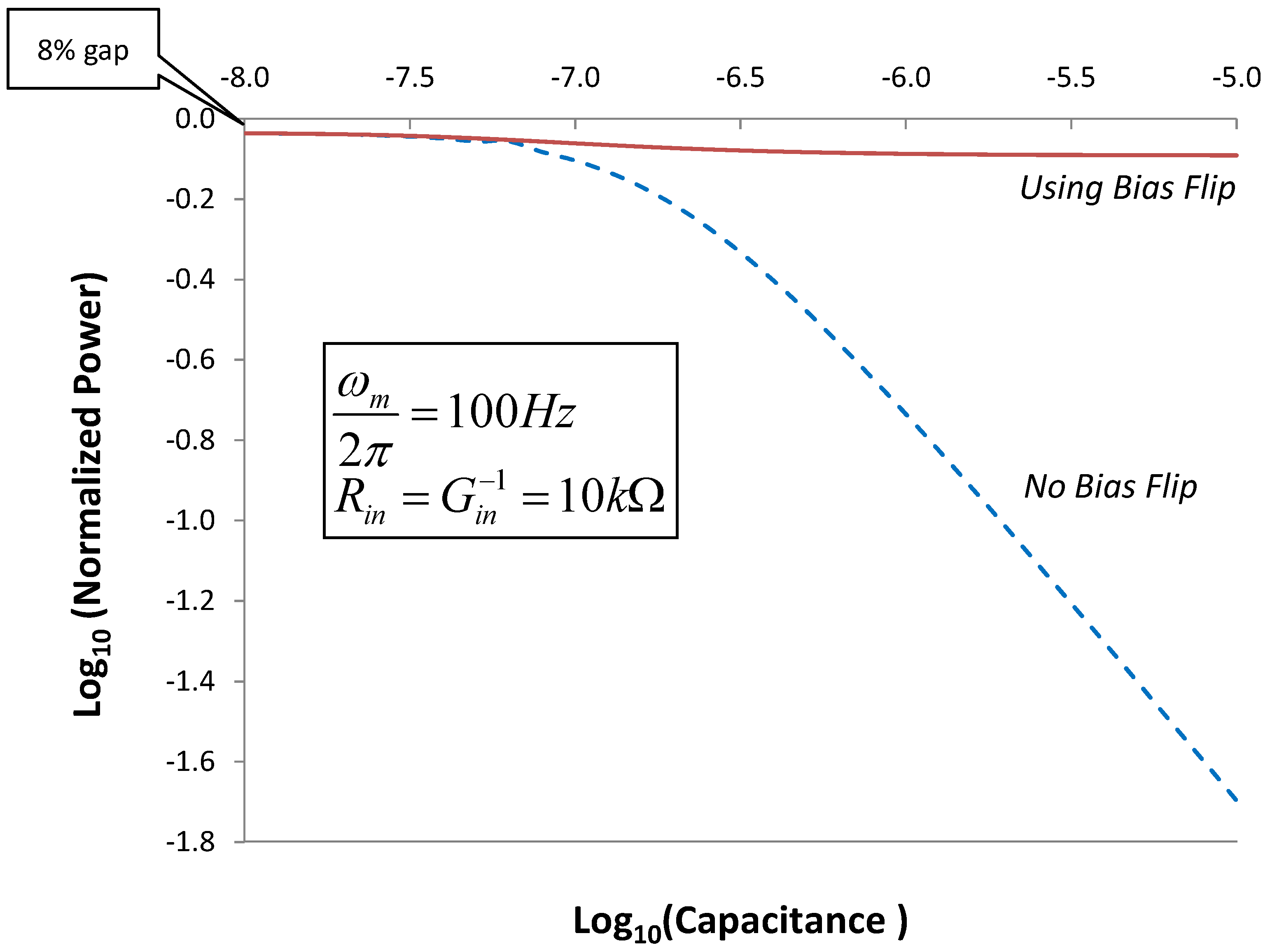
Figure 15.
Shows the rectified power as a function of
Cmc. For each point on the curve,
VRECT was selected to give the max power transfer. Power is normalized to
![Jlpea 03 00194 i061]()
, and capacitance has units Farads.
Figure 15.
Shows the rectified power as a function of
Cmc. For each point on the curve,
VRECT was selected to give the max power transfer. Power is normalized to
![Jlpea 03 00194 i061]()
, and capacitance has units Farads.
Figure 15 shows that, for large
Cmc, output is severely degraded. However, the Bias-Flip circuit is effective in recovering most of the lost output power. This analysis confirms the conclusions of Ramadass and Chandrakasan [
7] that for an EHD, operating at resonance, the Bias-Flip circuit is effective in canceling the reactive impedance of the device, and achieving near-optimum output power. In the next section, we will demonstrate that the Bias-Flip technique can be used to form an effective LC tank circuit that, when coupled to the EHD can tune the resonant frequency.
6. Bias Flip for Frequency Tuning
In
Section 5, we confirmed the effectiveness of the BF technique for power optimization at the mechanical resonant frequency. When
ω =
ωm, and the equivalent circuit of
Figure 3 applies, we can optimize power to the load by “canceling” or “matching” the reactive admittance of the capacitor with an inductor. We select an inductor value such that
![Jlpea 03 00194 i075]()
. Matching the reactive admittance aligns the phase of the voltage across the load with the phase of the current. This works because the current source is assumed to be ideal. Varying the reactive load does not change the current from the source. We confirmed the finding of [
7] that the BF inductor is effective in canceling capacitive admittance at
ωm. In this section, we will demonstrate that the BF inductor can also be used to tune the resonant frequency of the EHD and optimize power at frequencies substantially different from
ωm.
In order to maximize output power at any frequency, we need to maximize the input power delivered from the mechanical source to the EHD. In other words, we need to align the phase of the force with the phase of the source velocity.
In the following analysis, we assume the phase of
z(
t) to be zero.
![Jlpea 03 00194 i076]()
, and the velocity of the source is
![Jlpea 03 00194 i077]()
. The source velocity has a phase of +90
o. The force acting on the EHD is given by Equation (3). Our goal is to maximize.
Where
FI is the imaginary part of
F.
![Jlpea 03 00194 i078]()
. From this, we conclude that input average power is maximized when
F has phase +90°, matched to source velocity, and
X has phase −90°.
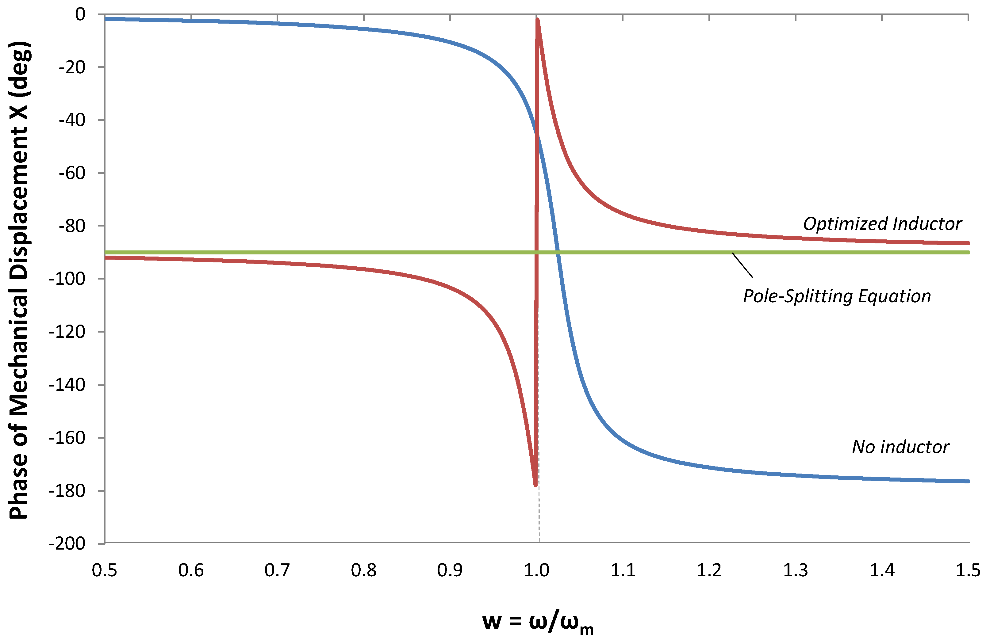
Figure 16.
Phase of mechanical displacement X(ω) for three cases: (1) No inductor; (2) Inductor optimized using (13) and (3) Inductor optimized using the pole-splitting Equation (9). In all three cases, GL = 0.
Figure 16.
Phase of mechanical displacement X(ω) for three cases: (1) No inductor; (2) Inductor optimized using (13) and (3) Inductor optimized using the pole-splitting Equation (9). In all three cases, GL = 0.
Additional insight into maximization of output power is seen in
Figure 16. Here, we compare the phase of mechanical displacement
X(
ω) for three conditions
No inductor. The phase is −90° only at
![Jlpea 03 00194 i079]()
. Below
ωm, the phase is ≈0°, and above
ωm, the phase is ≈ −180°. Only at
ω =
ωoc is the force in phase with the source velocity;
Inductor, optimized using Equation (13). Note that the phase approaches −90° above and below ω = ωm;
Inductor optimized using the pole-splitting Equation (9). The phase is −90° for all frequencies.
The improvement in power at frequencies above and below ωm results from phase alignment between force and source velocity.
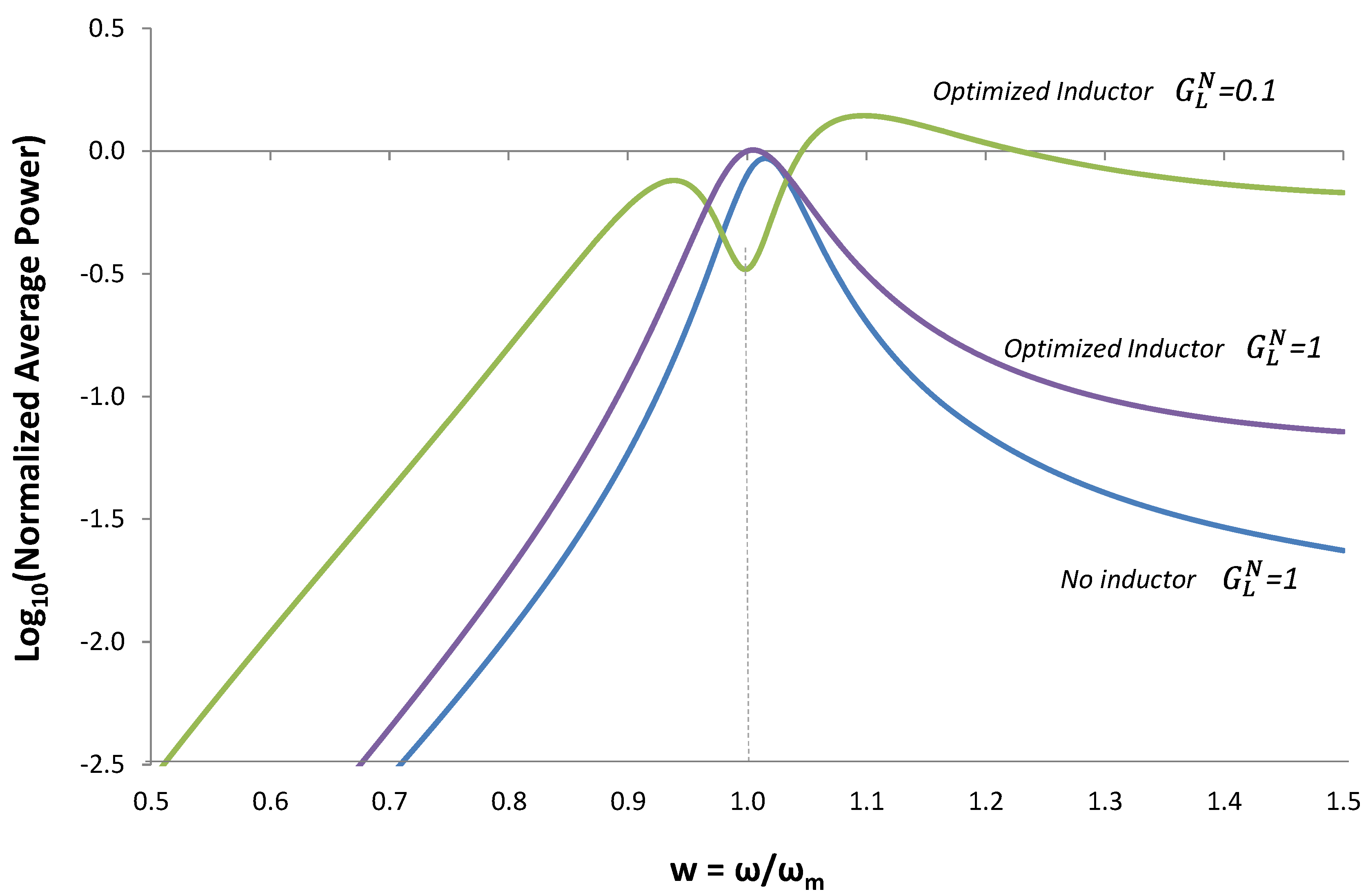
Figure 17 shows output power for 3 conditions.
No inductor:
![Jlpea 03 00194 i080]()
;
Inductor optimized using Equation (13):
![Jlpea 03 00194 i080]()
;
Inductor optimized using Equation (13):
![Jlpea 03 00194 i081]()
.
Figure 17.
Normalized Average Output Power for three cases. (1) No inductor &
![Jlpea 03 00194 i080]()
; (2) Inductor optimized using Equation (13) &
![Jlpea 03 00194 i080]()
; (3) Inductor optimized using Equation (13) &
![Jlpea 03 00194 i081]()
.
Figure 17.
Normalized Average Output Power for three cases. (1) No inductor &
![Jlpea 03 00194 i080]()
; (2) Inductor optimized using Equation (13) &
![Jlpea 03 00194 i080]()
; (3) Inductor optimized using Equation (13) &
![Jlpea 03 00194 i081]()
.
Case #2 illustrates the case where the reactive admittance is chosen to optimize output power, but the load conductance
![Jlpea 03 00194 i048]()
is kept at
![Jlpea 03 00194 i080]()
. Very little improvement is achieved, because the voltage is kept low by the high load conductance, and the voltage is ineffective in modulating the cantilever spring constant. Case #3 shows power improvement of ~50X compared to case #1. When we compensate for the increase in acceleration with frequency, case #3 demonstrates that it is possible to achieve output power at
ω ≠
ωm that is comparable to the maximum power at
ωm.
Additional insight into the mechanism of frequency tuning can be obtained by transforming the mechanical equations of motion to an equivalent circuit [
1,
8,
9], as shown in
Figure 18.
Figure 18.
(
a) Equivalent circuit model for a PZ EHD in which
![Jlpea 03 00194 i082]()
,
![Jlpea 03 00194 i083]()
,
![Jlpea 03 00194 i084]()
,
![Jlpea 03 00194 i085]()
,
![Jlpea 03 00194 i086]()
, and
![Jlpea 03 00194 i087]()
The subscript m denotes the mechanical circuit.
S(
ω) is used for velocity to avoid confusion with voltage; (
b) Equivalent circuit model of
Figure 18a, in which the electronic circuit is replaced by an electrical impedance Z
e.
The equations for the mechanical portion of the equivalent circuit are shown below.
Define
Zm to be the impedance seen by the voltage source
VF(
ω) in
Figure 18b. Setting Im(Z
m) = 0 gives the pole-splitting equation, equivalent to Equation (9), in the limit
![Jlpea 03 00194 i088]()
.
The last term in the above equation can be used to tune the resonance frequency above or below the mechanical resonance frequency. The last term takes the form
where
Leff can be made positive or negative to add or subtract from
Lm. At the mechanical resonance frequency
ω =
ωm,
![Jlpea 03 00194 i089]()
, and output power is optimized by setting
ω =
ωmc. When
ω <
ωm the resonant frequency
ω− must be reduced. This can be achieved by increasing the effective inductance, which can be achieved by setting
ωmc >
ω. When
ω >
ωm, the resonant frequency
ω+ must be increased. This can be achieved by decreasing the effective inductance, which can be achieved by setting
ωmc <
ω.
These results are summarized in
Table 1.
Table 1.
Strategy For Power Optimization in the Three Frequency Regions of Operation.
Table 1.
Strategy For Power Optimization in the Three Frequency Regions of Operation.
| Frequency region | Leff | ωmc | Phase of voltage | Optimum power |
|---|
| Region 1:
ω < ωm | >0 | ωmc > ω | ~ +90o | RL >> Rin |
| Region 2:
ω ≈ ωm | ≈0 | ωmc = ω ≈ ωm | ~0o | RL = Rin |
| Region 3:
ω > ωm | <0 | ωmc < ω | ~ −90o | RL >> Rin |
Maximizing power in the three regions can be envisioned in term of an effective inductor. Alternatively, it can be envisioned in terms of setting the phase of the voltage V(ω). The phase in each of the three regions is given in the table. In Region 2, the voltage across the load V(ω) is in phase with IS(ω), and output power is optimized by setting RL = Rin. However, in Regions 1 and 3, max power occurs when V(ω) has a phase of +90o (Region 1) and −90° (Region 3) relative to the phase of IS(ω), and optimum power is achieved by setting RL to be substantially larger than Rin.
The foregoing analysis suggests that the Bias-Flip technique can be used to synthesize an inductor, by flipping the polarity of the voltage in such a way that
X(
ω) has a phase of −90° in all three regions of operation. Recall from Equation (10) that, when
![Jlpea 03 00194 i048]()
is small, the phase of
X(
ω) is related to the phase of
V(
ω) in a simple way. By adjusting the phase of
V(
ω) as shown in
Table 1, we also adjust the phase of
X(
ω) to −90°.
Simulations were performed starting from the differential equations for v(t) and x(t) that are comparable to Equations (3) and (4), for the case of no inductor. These equations were solved subject to the boundary conditions.
In the case of no Bias-Flip,
![Jlpea 03 00194 i090]()
. The effect of the BF inductor is to change the phase of
v(
t) every half-period.
Using the voltage waveform, we calculated average output power. This is shown normalized to
![Jlpea 03 00194 i061]()
in
Figure 19. These simulations show that the BF technique is capable of achieving output power, comparable to the optimum power achievable with an optimized inductor. Moreover, the BF technique is self-tuning. If the bias is flipped whenever the source velocity crosses zero (as assumed in this simulation), the desired phase is maintained as the source frequency changes. No calculation is required to solve Equation (13).
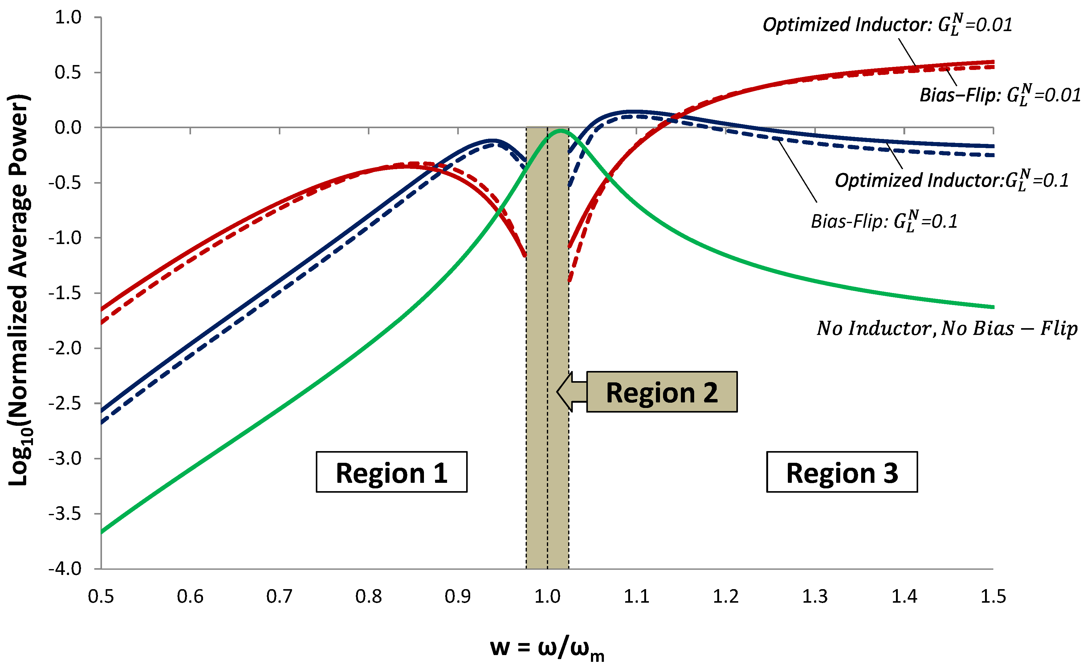
Figure 19.
Normalized average power as a function of frequency. In Regions 1 and 3, the Bias-Flip technique (red and blue dashed lines) improves output power by ~100X compared to the case of no inductor and no BF (green line). Moreover, it gives output power that is comparable to the maximum power achievable with an optimized inductor (red and blue solid lines).
Analysis of the voltage waveforms reveals another aspect of self-tuning. In Region 1, the bias flips from negative to positive at t = 0 and from positive to negative at t = T / 2, thereby emulating a +90° phase shift. In Region 3, the reverse happens. The bias flips from positive to negative at t = 0 and from negative to positive at t = T / 2, thus emulating a −90° phase shift.
7. Conclusions
In the preceding sections, we have explained the principles for electrically tuning of PZ EHDs. These principles are summarized below.
Equation (11) shows that the effective spring constant of the mechanical resonator is a function of voltage. If the load conductance is large, the voltage is kept small, and the resonator responds only at the mechanical resonant frequency ωm. However, for small load conductance GL, the voltage can be used to tune the spring constant, and the resonant frequency of the mechanical oscillator.
In Regions 1 and 3, output power is maximized by maximizing input power (force x velocity), transferred from the source to the EHD. At frequencies below ωm (Region 1), this occurs when the phase of the voltage is +90° relative to the source vibration, and at frequencies above ωm (Region 3), output power is optimized when the phase of the voltage is -90o relative to the source vibration.
This optimum phase relationship can, in theory, be achieved using a tunable inductor, whose value can be obtained from Equation (13). A large tunable inductor is not generally practical. However, the Bias-Flip technique can be used to emulate a large, tunable inductor. Previous work has shown that the BF technique can be used to optimize the output power at ωm, by cancelling the capacitive admittance of the EHD. In this work, we have shown how the BF technique can be used to tune an EHD and harvest energy from frequencies other than the mechanical resonance frequency.


 . The short-circuit, resonance frequency is given by
  . However, when the output is in the open circuit condition, D = 0; the open-circuit stiffness is given by
  , where ρ is the dimensionless PZ coupling constant, defined in Table 1. From this, it can be shown that the open-circuit and short-circuit resonant frequencies ωoc and ωm are related by the equation
  . This relationship is well-known, and has been used to experimentally determine the coupling constant ρ [1].
 for the case when there is no stress (σ = 0); and we define the motion constrained capacitance
  for the case when δ = 0.


 and
and  .
.

 . Throughout this paper, simulations are shown for ρ = 0.05; Qm = 20; and
  . These values are more representative of today’s commercial devices.
 . Frequency, on the horizontal axis, is normalized to ωm. For
  , Figure 4 confirms the predictions of Equation (7). For
  , the normalized voltage magnitude is 0.707; and for
  , the normalized voltage magnitude is 0.447. However, for w ≠ 1, Figure 4 shows interesting behavior, especially for
  . For
. For  .
. , the voltage peaks at the mechanical or short-circuit resonance frequency ωm. However, for small
  [4]. However, as we will see below, the addition of a resonant electrical circuit allows the voltage to swing below zero and above Voc, thereby enabling a wider tuning range.
  in the simulations above, the degradation is not large. However, in some cases, the PZ EHD has a large capacitance, which can substantially degrade output power at ω = ωm. In Figure 5, we simulate Equation (5) for the case ωmc = ωm. This is equivalent to adding an inductor that cancels the reactive admittance of the capacitor at ω = ωm. The inductor performs as expected at ω = ωm. The output voltage equals
  . Moreover, for large
  and
and  . These resonances result from the poles in the denominator of Equation (5) when
 . Pole splitting, which describes coupled modes of the mechanical and electrical resonators, occurs only for small
  is added to the circuit. Voltage is normalized as in Figure 4.

 and
and  are plotted vs.
  .
.


 . The important result is that the peak voltages away from resonance can be somewhat higher than
  indicates that output power peaks at ω = ωm, at the power
  given by Equation (8). The curve for
  shows a peak at ω = ωm at a degraded power level. The curve for
  shows two peaks at ω− and ω+ that have output power comparable to
  , the output power at ω− and ω+ decreases.
 is added to the circuit. Average power is normalized by
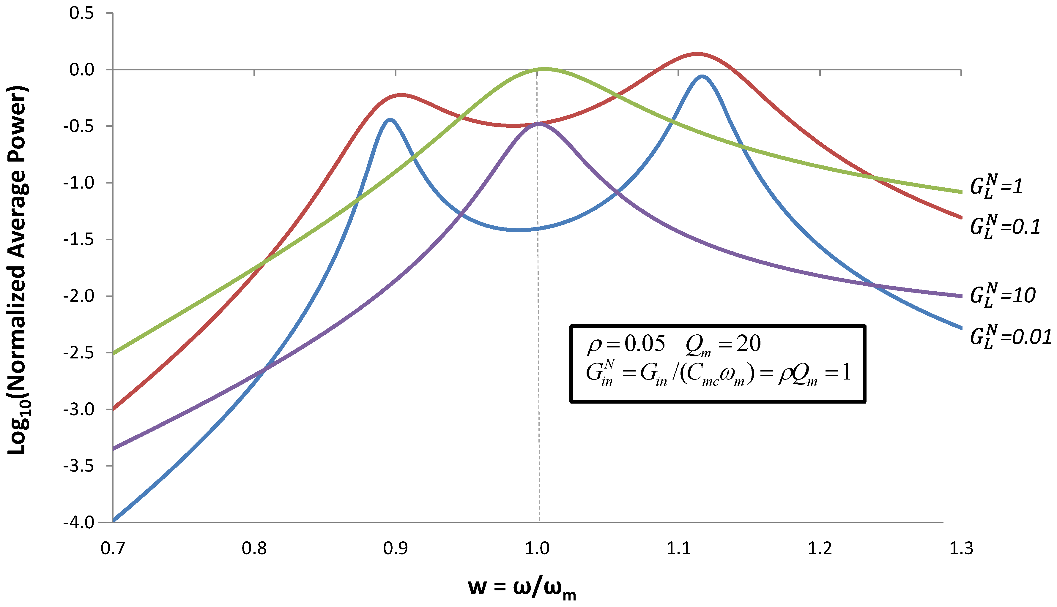
 in Equation (5) is equivalent to varying the inductor. Maximizing power with respect to ωmc gives the expression


 around the mechanical resonant frequency (Region 2), output power can be optimized by using (14) for reactive admittance and
  . In Regions 1 and 3, power is optimized by using the pole splitting Equation (9) for reactive admittance and
  . For the parameters used in this example (Qm = 20), Δw ≈ 0.025.
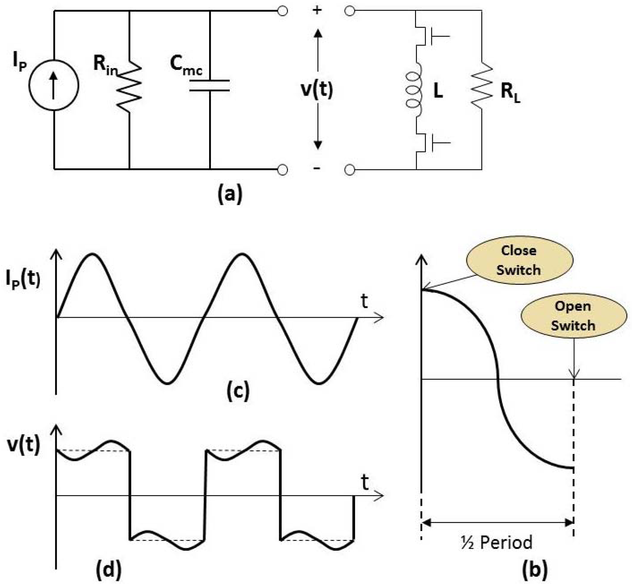
 . [See Equation (8)] In Figure 11, we show how effective the ideal Bias-Flip circuit is in achieving maximum power.
 , which is 8 / π2 = 81% of the max power obtained using an ideal inductor. This illustrates the effectiveness of Bias-Flip circuits to achieve high output power when Cmc is large [7].
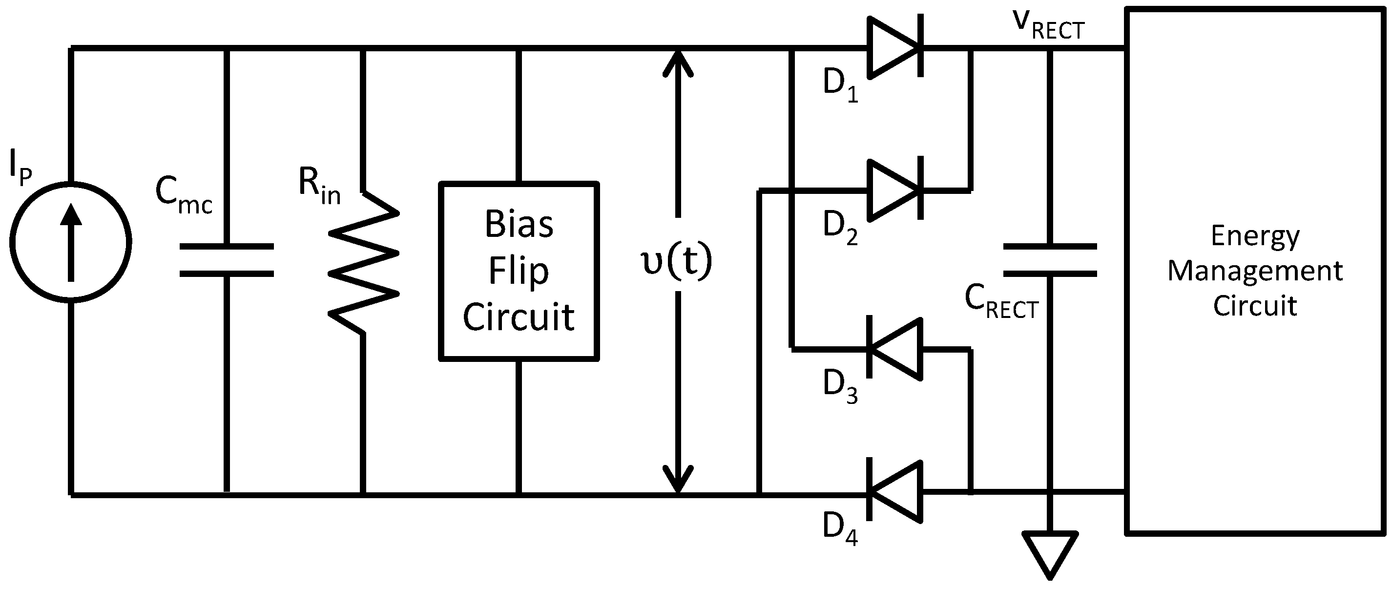
 until t = ton; at which time, v(t) becomes clamped at VRECT. Between ton and toff power is supplied to the storage unit. At t = toff, the diodes turn off, and v(t) returns to zero following the curve
  .
.
 and
and  .
.
 . Matching the reactive admittance aligns the phase of the voltage across the load with the phase of the current. This works because the current source is assumed to be ideal. Varying the reactive load does not change the current from the source. We confirmed the finding of [7] that the BF inductor is effective in canceling capacitive admittance at ωm. In this section, we will demonstrate that the BF inductor can also be used to tune the resonant frequency of the EHD and optimize power at frequencies substantially different from ωm.
 , and the velocity of the source is
  . The source velocity has a phase of +90o. The force acting on the EHD is given by Equation (3). Our goal is to maximize.
 . From this, we conclude that input average power is maximized when F has phase +90°, matched to source velocity, and X has phase −90°.

 ; (2) Inductor optimized using Equation (13) &
  .
.
 ,
,  ,
,  ,
,  ,
,  , and
, and  The subscript m denotes the mechanical circuit. S(ω) is used for velocity to avoid confusion with voltage; (b) Equivalent circuit model of Figure 18a, in which the electronic circuit is replaced by an electrical impedance Ze.


 .
.

 , and output power is optimized by setting ω = ωmc. When ω < ωm the resonant frequency ω− must be reduced. This can be achieved by increasing the effective inductance, which can be achieved by setting ωmc > ω. When ω > ωm, the resonant frequency ω+ must be increased. This can be achieved by decreasing the effective inductance, which can be achieved by setting ωmc < ω.

 . The effect of the BF inductor is to change the phase of v(t) every half-period.