1. Introduction
Subthreshold designs yield high energy efficiency by lowering operating voltages of the given circuits. Such designs can be applied to low-power sensor nodes or other low-power applications [
1]. On the other hand, several new-structure steep subthreshold slope (SS) FETs, such as FinFETs, Gate All Around (GAA) FETs, and tunnel FETs [
2,
3], have been discussed as further advancement of CMOS processes. These transistors have steeper SS values than conventional planar MOSFETs, and reduced leakage current at low voltages.
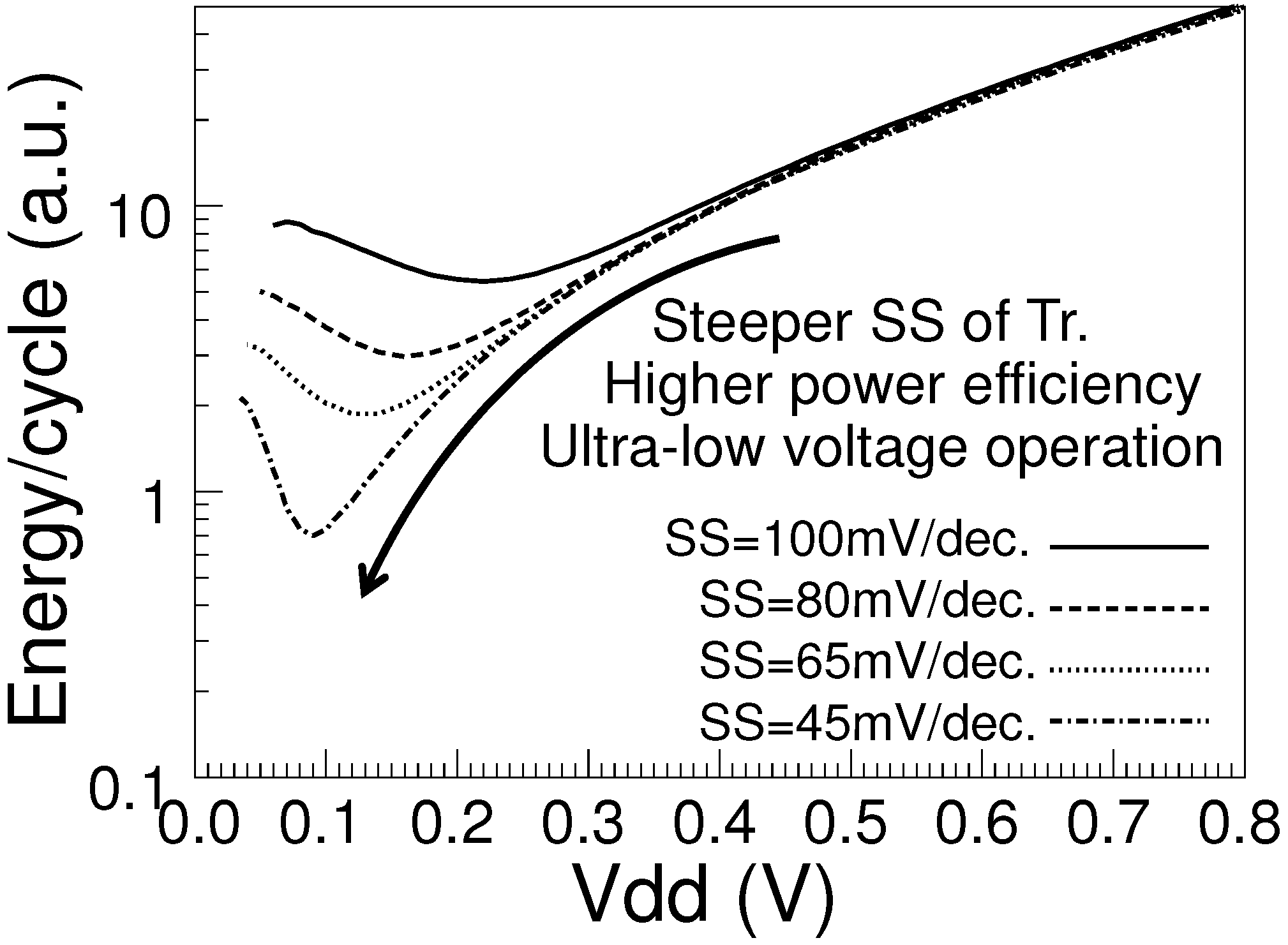
Figure 1 [
4] shows the energy/cycle of a 54-stage inverter chain under several SS conditions which was simulated following [
5]. From the figure, the SS of the planar CMOS process is approximately 100 mV/dec, with the minimum energy/cycle obtained at about 0.22 V. On the other hand, 3
× and 8.5
× energy efficiency improvement was obtained at near 0.1 V under 65 mV/dec and 45 mV/dec conditions because of reduced leakage current. In general, when the SS values of transistors are improved, the minimum energy point is lowered.
Figure 1.
Energy efficiency simulation results of inverter chains for various SS values.
Figure 1.
Energy efficiency simulation results of inverter chains for various SS values.
Lowering the operating voltage will be more effective for obtaining high energy efficiency in future processes: however, low-voltage operation is restricted by variability in transistor performance, and the impact of local random variation is serious in large-scale circuits [
5]. In [
6], Niiyama
et al. reported the minimum operating voltage of ring oscillators (ROs) in a 90-nm bulk process. Although the minimum operating voltage of 11-stage ROs was 90 mV, that of 1 million-stage ROs reached 343 mV. Several studies have reported on the implementation of ultra-low-voltage operation circuits [
7,
8,
9,
10]; their operating ranges are from 0.175 V to 0.28 V depending on the scale of the circuit and process technology. SRAM has relatively high minimum operating voltage, and methods of lowering the minimum operating voltage via circuit structures are frequently discussed in the literature. A conventional 6T-SRAM has approximately 0.8 V minimum operating voltage [
11], whereas 7T [
12], 8T [
13], 10T [
14], and improved-6T [
15] SRAMs operate at 0.44 V, 0.25 V, 0.16 V and 0.208 V, respectively.
In this study, we report notably decreased minimum operating voltages via variability suppressed Silicon on Thin Buried Oxide (SOTB) [
16] technology with a million-gate logic circuit based on our previous research [
17].
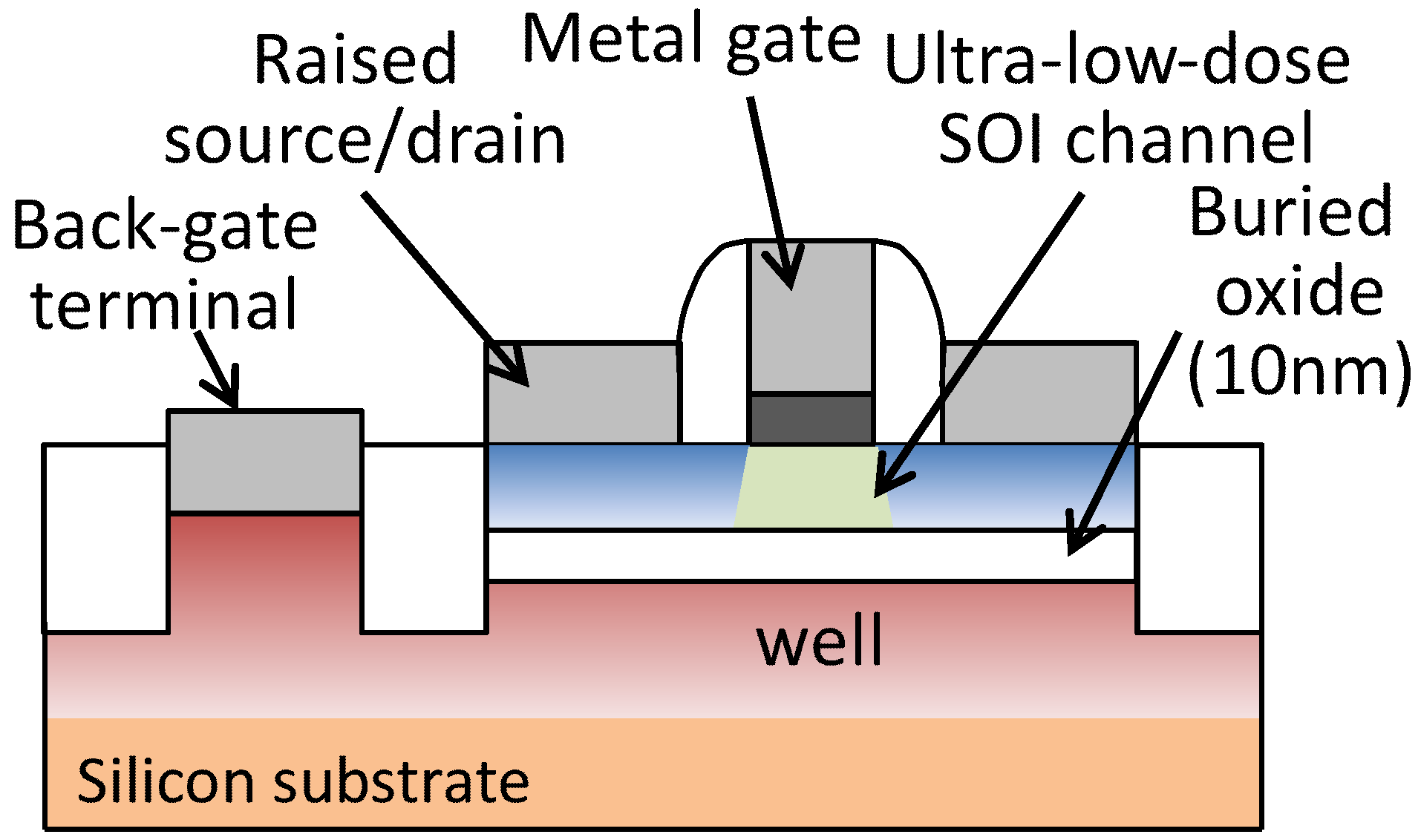
Figure 2 shows the structure of the SOTB transistor, which is formed on a thin silicon on insulator (SOI) layer and has an ultra-low dose channel. This ultra-low dose channel enables reductions in the random dopant variability and, as a result, decreased operating voltage is expected. Whereas a 0.37 V minimum operating voltage of 6T-SRAM in the SOTB process has been reported [
11], we focus on logic circuits. We measure a 1 million-gate logic circuit consisting of 1011 ROs with 1001 stages on test chips fabricated in 65-nm SOTB and bulk processes, and demonstrate the notable impact of low-variability SOTB technology on ultra-low-voltage design. In addition, the operating voltage limit of logic circuits is the fundamental limit of the minimum operating voltage of SRAMs. Our measurement results on the operating voltage limit of logic circuits in bulk and SOTB processes suggest the goal of research on the reduction of the minimum operating voltage of SRAMs in the common bulk, SOTB, or other variability-suppressed processes.
Figure 2.
Schematic cross section of Silicon on Thin Buried Oxide (SOTB) transistor.
Figure 2.
Schematic cross section of Silicon on Thin Buried Oxide (SOTB) transistor.
2. Implementation of Test Element Group (TEG)
We designed 337 RO patterns, and each RO pattern consists of 3 ROs. An RO pulse is counted by the counter on the chip. To measure ultra-low-voltage operation of ROs, we implemented three power supply and ground-line pairs for ROs, a counter and buffers. The buffers were located between the ROs and the counter.
Table 1 describes the details of the implemented 337 ROs. We selected INV, NAND, and NOR gates as measurement target gates. Our nominal design of INV, NAND and NOR cells had 1:1, 1:1 and 2:1 P:N (pMOS width:nMOS width) ratios, respectively. In addition to basic logic cells, complex gates are commonly included in standard cell libraries, and these complex gates frequently include serially stacked transistors, transmission gates, or an unbalanced P:N ratio. The impact of these designs in a low-voltage design is different from that of a MOS width (W) change. Although we observe ultra-low-voltage operation of 1 million logic gates with this RO Test Element Group (TEG), this TEG is also aimed to be designed for observation of layout dependence [
18]. Gates in which shallow trench isolation (STI) stress effect and inverse narrow channel effect were escalated were included in the RO patterns. The stress caused by STI causes a mobility shift of pMOS and nMOS transistors depending on the distance between the transistor gate and STI edge. The inverse narrow channel effect is the reduction of
observed in narrow channel device. These effects can cause
or mobility variation, and are beneficial for estimating low-voltage behavior of logic circuits.
Table 1.
Number of designed ring oscillator (RO) patterns; 3 ROs for each RO design were placed on a chip.
Table 1.
Number of designed ring oscillator (RO) patterns; 3 ROs for each RO design were placed on a chip.
| Included Gate(s) | Number of RO Designs Containing |
|---|
| Single Type | 2 Types | 3 Types |
|---|
| Basic | STI | Narrow
Channel | Basic | STI | Narrow
Channel | STI | Narrow
Channel |
|---|
| INV | 1 | 7 | 6 | - | 22 | 21 | - | 20 |
| NAND | 1 | 7 | 13 | - | 22 | 18 | - | - |
| NOR | 1 | 7 | 10 | - | 22 | 18 | - | - |
| INV & NAND | - | - | - | 1 | 29 | 15 | - | - |
| INV & NOR | - | - | - | 1 | 29 | 15 | - | - |
| NAND & NOR | - | - | - | 1 | 29 | 21 | - | - |
Changes in STI effect were implemented with active area design. Each standard cell consisted of an even number of pMOS or nMOS transistor, and their sources or drains, which are connected to ground or power, were connected to neighboring gates. When a source or drain area of a pMOS or nMOS transistor is connected to that of neighboring gates, STI is not inserted between the gates, and the impact of STI in the gate width direction can be weakened. The strength of the inverse narrow channel effect can be escalated by narrowing the transistor width.
Table 2 shows implemented STI conditions in the gates. We designed four STI conditions,
i.e., (pMOS STI weak, nMOS STI weak), (pMOS STI weak, nMOS STI strong), (pMOS STI strong, nMOS STI weak) and (pMOS STI strong, nMOS STI strong), for INV, NAND and NOR cells. In addition to changing STI conditions, simple transistor width changes were also implemented such that the impact of STI could be compensated. The STI stress effect is known as nMOS mobility degradation and pMOS mobility enhancement, and (pMOS nominal W, nMOS W +10%) and (pMOS nominal W, nMOS W +20%) patterns were additionally designed for (pMOS STI weak, nMOS STI strong) and (pMOS STI strong, nMOS STI weak) designs.
We also designed the gates with narrow channel transistors as shown in
Table 3. We set 1/n
× width per finger and n
× number of fingers for cells to observe narrow channel effects, and enhanced the narrow channel effect without changing the total transistor width in each cell. We used this approach because simply narrowing the width causes a reduction of driving current of transistors, and the narrow channel effect and reduction of width would otherwise be confused in our measurement results. Implemented (width per finger, number of fingers) patterns were (1/1.5
× width per finger, 1.5
× number of fingers), (1/2
× width per finger, 2
× number of fingers), and (1/3
× width per finger, 3
× number of fingers). The pMOS and nMOS conditions of narrow channel cells includes (pMOS nominal width, nMOS narrow width) and (pMOS narrow width, nMOS narrow width).
An RO consisting of only one type of cell may report too optimistic a minimum operating voltage and, in addition to ROs with one type of cell, ROs which include two or three types of cells were also designed. The details of the number of RO patterns are shown in
Table 1. 53 patterns of ROs included a single type of cell, whereas 284 patterns were composed of two or three cells.
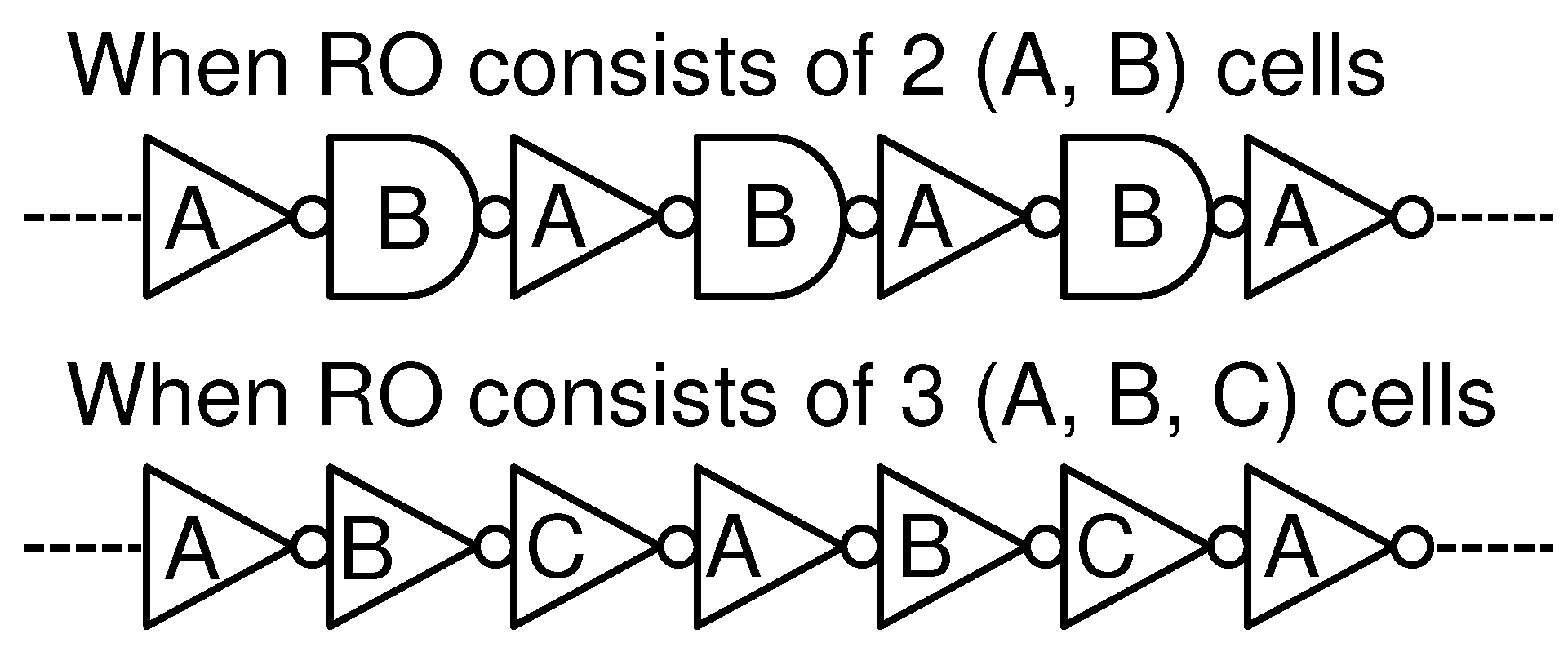
Figure 3 shows the connection of cells when an RO included two or three types of cells. When two types of cells were included in an RO, the cells were organized in an alternating pattern. When an RO had three types of cells, these cells repetitively appear in the order shown in
Figure 3. Six RO patterns were designed only with basic INV, NAND, and NOR cells. Moreover, 174 RO patterns included cells where STI conditions were modified. Among the 174 STI RO patterns, 21 consisted of a single type of cell and 153 ROs include two types of cells. Cells with narrow channel conditions were inserted in 157 RO patterns, among which were 29 ROs with a single type of cell, 108 ROs with two types of cells, and 20 ROs with three types of INV cells. Furthermore, 108 ROs with two types of narrow channel cells include 21 ROs with two types of INV cells, 18 ROs with two types of NAND cells, 18 ROs with two types of NOR cells, 15 ROs with INV and NAND cells, 15 ROs with INV and NOR cells, and 21 ROs with NAND and NOR cells.
Table 2.
Implementation of escalation of shallow trench isolation (STI) stress effect in the gates.
Table 2.
Implementation of escalation of shallow trench isolation (STI) stress effect in the gates.
| Gate Design | pMOS | nMOS |
|---|
| Active Area | Width | Active Area | Width |
|---|
| nominal design | connected | nominal | connected | nominal |
| to neighboring gate | to neighboring gate |
| STI stress #1 | NOT connected | nominal | connected | nominal |
| to neighboring gate | to neighboring gate |
| STI stress #2 | NOT connected | nominal | connected | +10% |
| to neighboring gate | to neighboring gate |
| STI stress #3 | NOT connected | nominal | connected | +20% |
| to neighboring gate | to neighboring gate |
| STI stress #4 | connected | nominal | NOT connected | nominal |
| to neighboring gate | to neighboring gate |
| STI stress #5 | connected | nominal | NOT connected | +10% |
| to neighboring gate | to neighboring gate |
| STI stress #6 | connected | nominal | NOT connected | +20% |
| to neighboring gate | to neighboring gate |
| STI stress #7 | NOT connected | nominal | NOT connected | nominal |
| to neighboring gate | to neighboring gate |
Table 3.
Implementation of escalation of inverse narrow channel effect in the gates.
Table 3.
Implementation of escalation of inverse narrow channel effect in the gates.
| Gate Design | pMOS | nMOS |
|---|
| Width | Number of Fingers | Width | Number of Fingers |
|---|
| nominal | nominal | nominal | nominal | nominal |
| narrow channel #1 | nominal | nominal | 1/1.5× | 1.5× |
| narrow channel #2 | 1/1.5× | 1.5× | 1/1.5× | 1.5× |
| narrow channel #3 | nominal | nominal | 1/2× | 2× |
| narrow channel #4 | 1/2× | 2× | 1/2× | 2× |
| narrow channel #5 | nominal | nominal | 1/3× | 3× |
| narrow channel #6 | 1/3× | 3× | 1/3× | 3× |
Figure 3.
The gate connection in RO when RO includes two or three cell patterns.
Figure 3.
The gate connection in RO when RO includes two or three cell patterns.
Each RO consisted of 1000-stage measurement target gates and 1 NAND gate for controlling oscillation. There were trade-offs between implementation costs of glue logic and granularity of yield evaluation. The 1-million gate measurement structure can be implemented with a 1000-to-1 selector and 1000 output wires from ROs by adopting 1001-stage ROs. The implemented 1011-to-1 selector consists of 1010 multiplexer cells, and does not include a notably large number of cells in comparison with 1001-stage RO.
Although the routing of 1011 wires was a bottleneck of the layout of the selector circuit and required 0.964 mm
area on the test chip with the automated place and route software [
19], the area cost of routing was acceptable because we had 12.5 mm
area on the chip. Had we adopted 101-stage ROs, we would have required a 10000-to-1 selector, which consists of 9999 multiplexer cells, and 10,000 wires. Compared to the chosen implementation of the 1011-to-1 selector and 1011 wires, the area cost for the implementation of 9999 cells and 10,000 wires would have been unacceptable for our test chip. Consequently, we avoid the huge area cost of a selector circuit and wiring cost of RO control and output signals by adopting 1001-stage ROs. Though the yield of a small-size circuit becomes difficult to be identified when too large RO size is adopted, yields of 1 million gates, 100,000 gates and 10,000 gates can easily be calculated from the measurement results of the 1001-stage ROs. These circuit scales are suitable for practical use of Application Specific Integrated Circuits (ASIC) or System on Chip (SoC) applications.
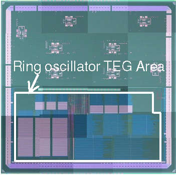
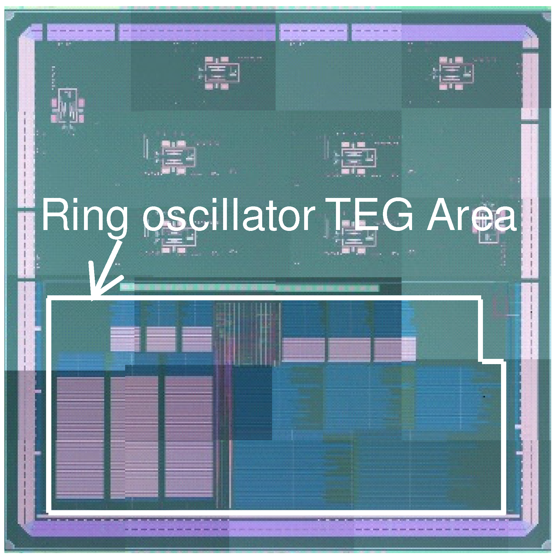
Figure 4.
A micrograph of the test chip.
Figure 4.
A micrograph of the test chip.
The test chips were fabricated in 65-nm SOTB and bulk processes.
Figure 4 shows the micrograph of the fabricated test chip. The size of the test chips is 5.8 mm
× 5.8 mm, with an area of approximately 5.0 mm
× 2.5 mm allocated for the RO TEG.
4. Variability in SOTB and Bulk Processes
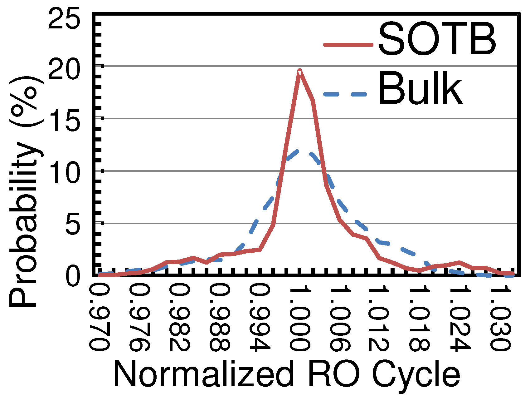
In this section, we evaluate the process variability of bulk and SOTB processes based on measured RO periods. RO periods on SOTB and bulk chips were measured at 0.4 V and 0.55 V respectively. As of SOTB and bulk transistors were different, we compared RO periods of SOTB and bulk chips at supply voltages where the same RO period was obtained. The periods of basic ROs of SOTB at 0.4 V and bulk at 0.55 V were approximately 500 ns.
Figure 5 shows a histogram of measured RO periods. RO periods were normalized by averaging RO periods of each pattern. Each pattern had 3 ROs on each chip, and 12 ROs of each pattern on 4 chips were used for calculating the average value, and periods of 12 ROs were normalized by the calculated average of each pattern. The probabilities of SOTB were notably higher than that of bulk in the RO periods ranging from 0.998 to 1.002, and clearly lower in the range from 0.992 to 0.996 and the range from 1.004 to 1.018. The distribution of RO periods was more concentrated on the average period in the SOTB process than that of the bulk process and, thus, we confirmed smaller local random variability in the SOTB process. Although notable differences were not observed in ranges below 0.990 and above 1.020 between SOTB and bulk results, distributions in these ranges can be considered to be caused by the impact of global variability, which is not improved by SOTB technology.
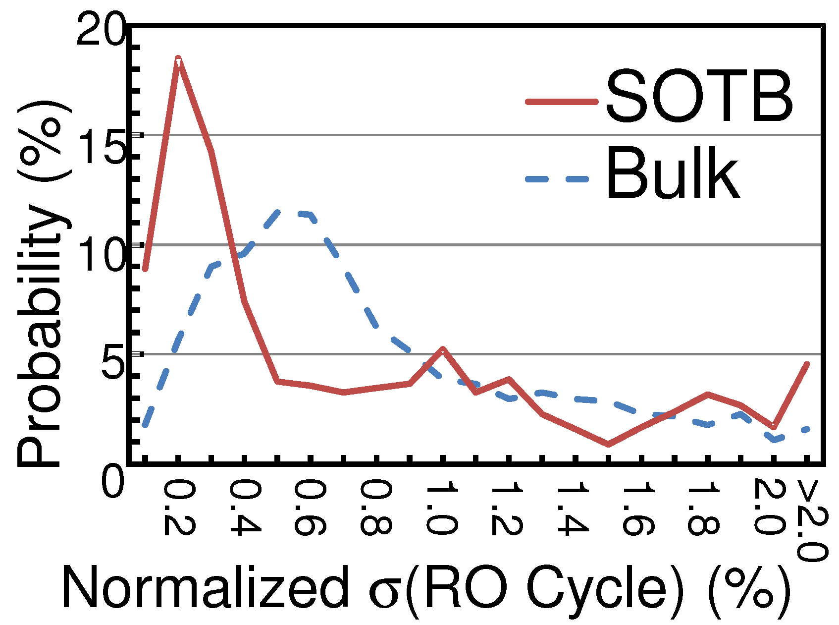
We also calculated the standard deviations (σ) of RO periods for each of the 337 RO patterns on each chip, and
Figure 6 shows the histogram of the calculated σ values. For each RO pattern, 3 ROs were implemented on each chip, and standard deviations of each pattern on each chip were calculated to eliminate the impact of global variability from standard deviations. Each standard deviation value was normalized by the average period of 3 ROs of each pattern on each chip. The peaks of σ distribution of SOTB and bulk were 0.2% and 0.5% respectively. The σ distribution of SOTB was larger than that of bulk in the range from 0.1% to 0.3%, and smaller in the range from 0.4% to 1%. The σ values of SOTB concentrate in a smaller range, and small random variability of SOTB was also confirmed, as in the results of average RO period. Both
Figure 5 and
Figure 6 indicate low variability of the SOTB process in comparison with the bulk process.
Figure 5.
Measured RO periods on SOTB and bulk chips at 0.4 V and 0.55 V respectively.
Figure 5.
Measured RO periods on SOTB and bulk chips at 0.4 V and 0.55 V respectively.
Figure 6.
Standard deviations of period of each RO pattern on each chip.
Figure 6.
Standard deviations of period of each RO pattern on each chip.
5. Low-Voltage Operation
1011 ROs with 1001-stages on test chips fabricated both in bulk and SOTB processes were measured. The
mismatch between pMOS and nMOS transistors can be one of the factors that deteriorates circuit operating voltages, and considerable efforts are therefore devoted to minimize this
mismatch in process development; however, at near
0.1 V, the margin of
mismatch is very small, and even the slight
mismatch has a serious impact. We tested several back-gate bias conditions, identifying back-gate bias conditions that minimized operation failure for bulk and SOTB chips. Our results for the applied back-gate bias conditions include:
Bulk-a:
Bulk-b:
SOTB-a:
SOTB-b:
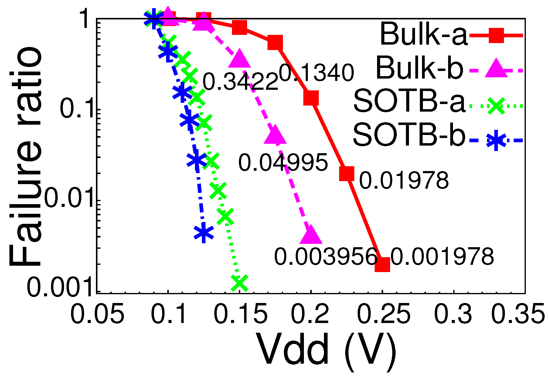
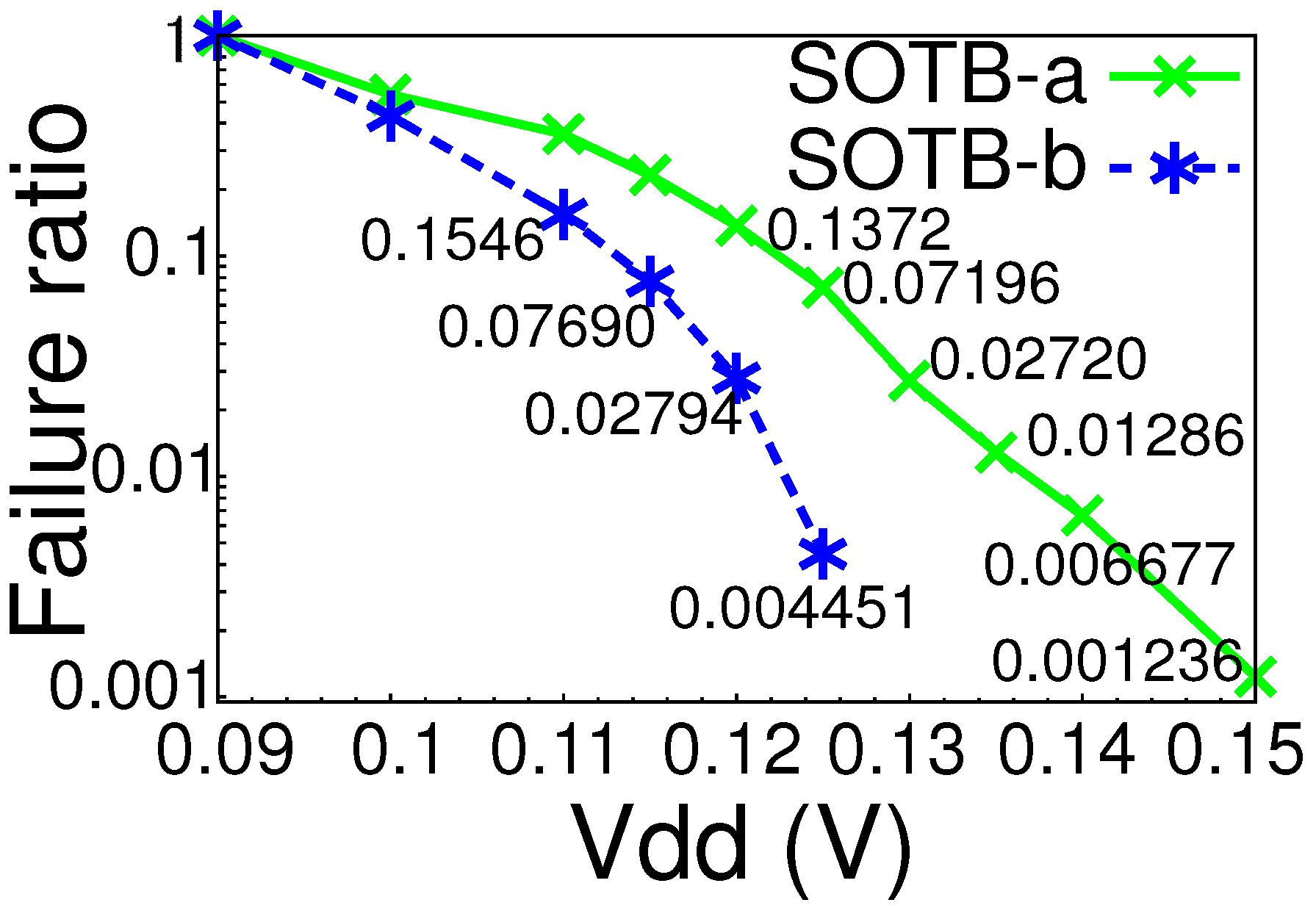
VBP and VBN are pMOS and nMOS back-gate bias voltages. Furthermore, in conditions b, back-gate bias voltages were applied to compensate for mismatch, whereas in conditions a, the back-gate bias voltages were applied equally to pMOS and nMOS transistors, and the back-gate bias voltages were not applied to compensate for mismatch. When reverse body bias voltages were not applied, the RO period on bulk and SOTB chips were 307.5 μs and 4.36 μs, respectively, at = 0.2 V. The RO period in Bulk-b, SOTB-a and SOTB-b conditions increased to 902.5 μs, 11.1 μs and 14.0 μs at = 0.2 V, respectively.
Figure 7 and
Figure 8 show the measurement result of the RO operation. In these figures, the x-axis is the supply voltage and the y-axis is the ratio of the number of ROs that failed to operate. The yield of 10 k-gate and 100 k-gate circuits can be calculated as
and
, respectively where
Y is the failure ratio. When the back-gate bias voltages were equally applied for pMOS and nMOS transistors, the first failures were observed at 0.25 V and 0.15 V for bulk and SOTB, respectively. The failure rates at this voltage enabled a practical yield of a 100 k-gate circuit. A 0.072 failure ratio of SOTB at 0.125 V corresponds to approximately 47.3% yield of a 10 k-gate circuit, whereas 0.225 V is required for the bulk process to obtain this yield. Adjusting the back-gate bias lowered the first failure voltages to 0.2 V and 0.125 V for bulk and SOTB, respectively. Over 40% yield for a 10 k-gate circuit is achieved at 0.115 V in the SOTB process whereas 0.175 V was required for the bulk process.
Figure 7.
Measurement results of the RO operation. Y-axis is the ratio of the number of ROs which failed to operate.
Figure 7.
Measurement results of the RO operation. Y-axis is the ratio of the number of ROs which failed to operate.
These measurement results confirmed that the low variability of SOTB notably lowers the minimum operating voltage of a large scale logic circuit, and the low-variability of SOTB technology enables near-0.1 V operation of logic circuits. At near 0.1 V, the margin against mismatch is seriously small in comparison with 0.2 V- to 0.4 V-class low-voltage operation. Even control by the foundries for low-voltage operation will not sufficiently eliminate this mismatch. Measurement results also indicate that back-gate biasing is effective for obtaining operation margin in extremely low-voltage and small--margin conditions.
Here, the limit of the operating voltage on the bulk process was 0.175 V–0.25 V according to our measurement results. The limit of operating voltage of several improved SRAMs reported in [
13,
14,
15], 0.16 V–0.25 V, has already reached our measured limit of the operating voltage of the logic circuits. The operating voltage of SRAM cannot be fundamentally reduced beyond that of logic circuits, and further lowering of the operating voltage of SRAM is estimated to be difficult.
Figure 8.
Measurement results of SOTB process at = 0.09 V–0.15 V.
Figure 8.
Measurement results of SOTB process at = 0.09 V–0.15 V.
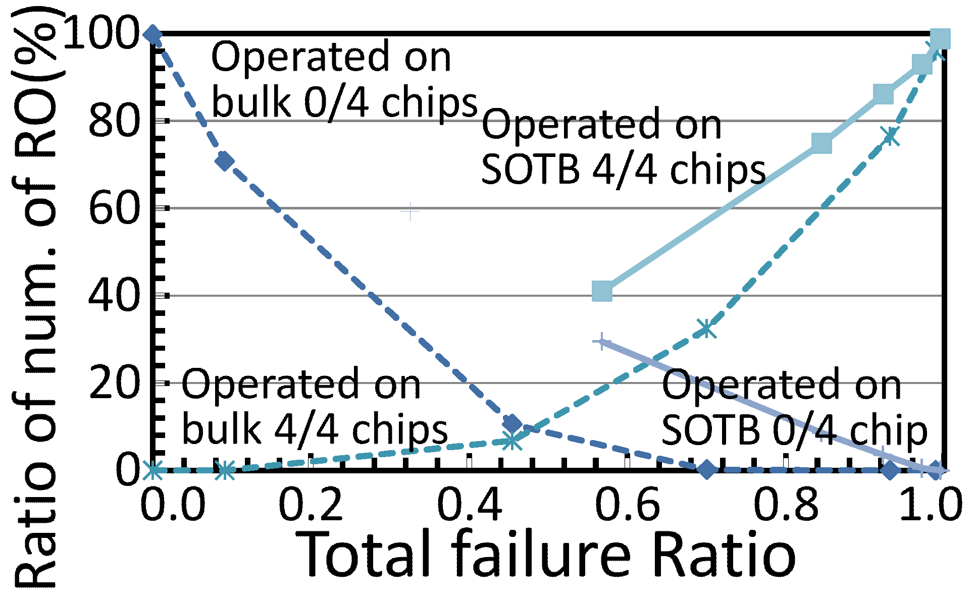
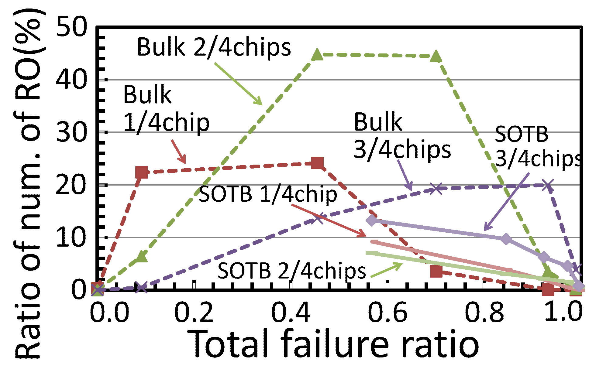
We also focused on the tendency of 1011 ROs to operate successfully. Here we numbered 1011 ROs serially, and 3 ROs on each pattern on each chip were identified by the location. We measured 4 bulk chips and 4 SOTB chips, and the number of chips where specific ROs operate is from 0 to 4, depending on supply voltages. For example, in the case of bulk 0.15 V operation, the total failure ratio was 0.455 with 6.8% of ROs operating on all 4 chips, 13.6% of ROs operating on 3 chips, 44.8% of ROs operating on 2 chips, 24.1% of ROs operating on 1 chip, and 10.6% of ROs failing on all 4 chips. The number of chips with a specific RO operating successfully strongly depends on the total failure ratio; therefore, the total failure ratio was also considered in our evaluation. In
Figure 9 and
Figure 10, the tendencies of bulk-b and SOTB-b conditions were demonstrated, with x-axis representing the total failure ratio, and the y-axis representing the ratio of the number of ROs operating on 0, 1, 2, 3, and 4 chips.
In
Figure 9 and
Figure 10, the number of ROs operating on 1, 2, or 3 chips in the bulk test chip is larger than that in the SOTB test chip, and number of ROs operating on 0 or 4 chips in the bulk test chip is smaller than that in the SOTB test chip. This tendency indicates that RO operation failure tends to be random in bulk chips, and deterministic in SOTB chips. In particular, the cause of RO operation failure in bulk chips can be considered to be random variability. Conversely, in SOTB chips, the bottleneck of the operating voltage can be thought to be a gate design problem rather than random variability. These results indicate that random variability of the SOTB process is smaller than that estimated from the observed operating voltage and that the operating voltage of the SOTB process can be further decreased by optimizing the gate design.
Figure 9.
Distribution of the number of ROs operated on 0 or 4 chips; the x-axis is the total operation ratio illustrated in
Figure 7 and
Figure 8.
Figure 9.
Distribution of the number of ROs operated on 0 or 4 chips; the x-axis is the total operation ratio illustrated in
Figure 7 and
Figure 8.
Figure 10.
Distribution of the number of ROs operated on 1, 2, or 3 chips; the x-axis is the total operation ratio shown in
Figure 7 and
Figure 8.
Figure 10.
Distribution of the number of ROs operated on 1, 2, or 3 chips; the x-axis is the total operation ratio shown in
Figure 7 and
Figure 8.


