This paper discusses scaling of Floating-Gate (FG) devices, and the resulting implication to larger systems, such as large-scale Field Programmable Analog Arrays (FPAA).
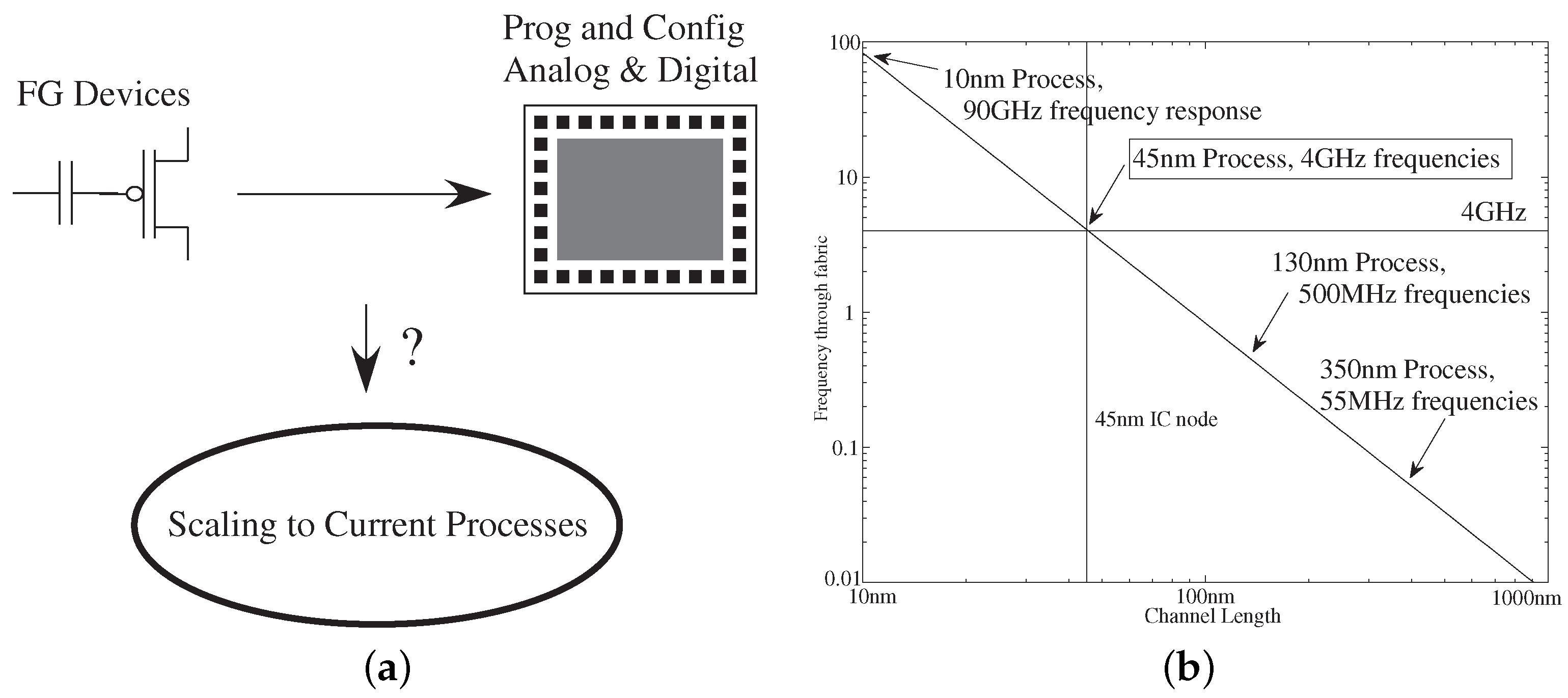
Figure 1 shows our high level figure, connecting the properties of FG circuits and systems in one technology (e.g., 350 nm CMOS), and predicting the behavior and advantages in smaller technologies. FG devices have been essential in demonstrating programmable and configurable analog and mixed mode computation, although typically at processes like 350 nm CMOS. The question of scaling these devices to more modern processes (e.g., 130 nm, 40 nm CMOS), typical of other system Integrated Circuits (IC) (e.g., FPGAs) remains, even though Electrically Erasable ROMs (EEPROMs) have moved to smaller and smaller linewidths (<20 nm gate length), and continued growth is expected.
Figure 1 shows scaling FG devices to smaller line widths results in higher frequencies enabled through an FPAA fabric, as well as lower FPAA power consumption, due to lower parasitic capacitances. Scaling of FG devices is a key issue when working to improve the density as well as raising the density of FG based memories, computing in memory systems, and FPAA. For example, how will an FPAA’s operating frequency improve as the IC technology process is scaled down?
Figure 1 shows a modeling summary of the capability at the frequency of a particular FPAA device architecture as a function of process geometry used. Although the initial FPAA devices, built in 350 nm process, have achieved frequencies in the 50–100 MHz range (i.e., [
7]), scaled FPAA devices should enable significantly higher frequencies, enabling RF type signals at 40 nm and smaller IC processes. Therefore, the potential of scaled down devices, and the resulting computation, from a 350 nm process down to a 40 nm process, requires investigating both experimentally and analytically the effects of a 40 nm process.
1. 350 nm FG Devices as Baseline for Scaling Performance
This section addresses what is needed for a functional FG device, typical of a wide range of circuit applications [
7,
8,
9], as well as how these processes are characterized.
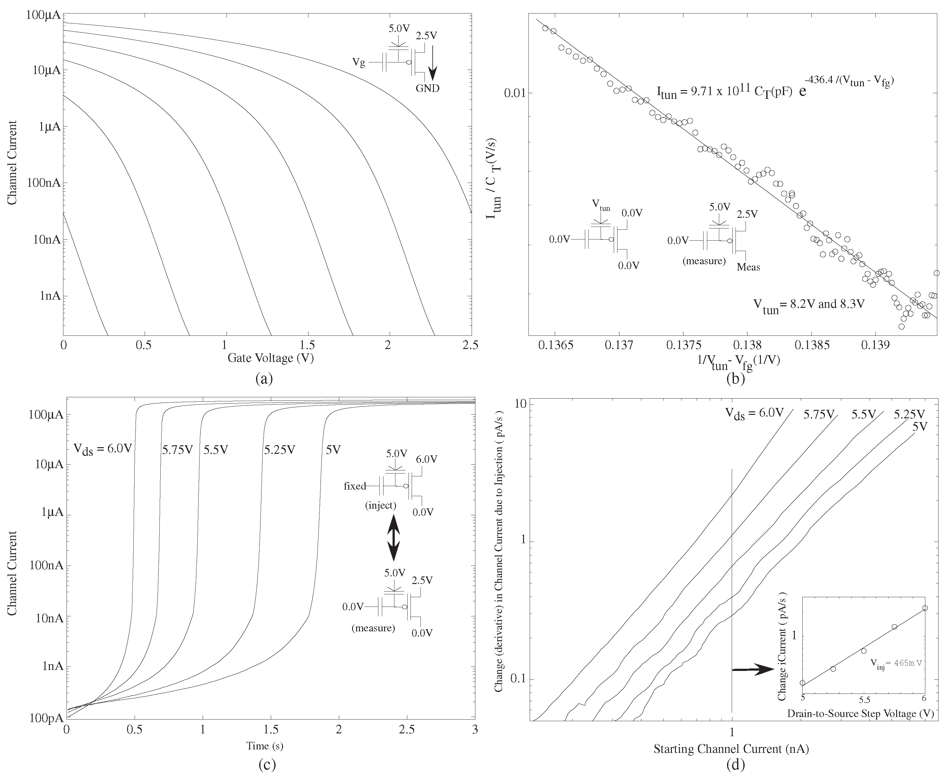
Figure 2 shows the fundamental plots to characterize the resulting FG devices, enabling an automated FG algorithm [
10].
Figure 2a shows that the current–voltage relationship is programmed through stored FG charge, resulting in a programmable weighting factor (i.e., subthreshold) and/or a programmable threshold voltage (
V, i.e., above-threshold). Although one has a capacitive divider, we have typical current–voltage relationships for a single curve. Changing the FG charge moves to a different curve, either increasing it by electron tunneling, or decreasing it by hot-electron injection. The resulting charge results in a voltage change on the FG node by the total capacitance at the FG node, or
C, the sum of all capacitances at the FG node. An FG pFET transistor has a similar behavior to a pFET device, but with a different effective value for the subthreshold slope (
for a typical FET device, where
κ is the capacitive voltage divider between gate and surface potential, and
is the thermal voltage (kT/q) ) due to the capacitive divider, the incoming (
gate) capacitance and (
), and a programmable flatband voltage that can move the curve throughout the voltage range.
Because of the high quality gate insulators, the FG charge, once programmed, will remain roughly unchanged months and years later (at the same temperature) (e.g., [
8,
9]). We expect a typical FG device to change 1–100
V at room temperature over a 10 year device lifetime as characterized by accelerated temperature measurements for this 350 nm CMOS process [
9]. Long-term charge loss in floating-gate transistors occurs due to the phenomenon of thermionic emission, classically described by the simple model [
11,
12,
13,
14]
where
Q(0) is the initial charge on the floating-gate,
Q(
t) is the floating-gate charge at time
t,
v is the relaxation frequency of electrons in polysilicon, and
is the effective Si-insulator barrier potential (Volts). In [
8], it has been shown that this model overestimates the charge loss, and that it does not follow such a simple curve, but a classical starting point.
Figure 2b shows characterization of electron tunneling for an FG pFET in this 350 nm CMOS process. Electron tunneling adds a charge at the floating gate [
15,
17]. Tunneling current increases the resulting FG voltage, decreasing the resulting current measured from a pFET device connected to this FG [
15]. The tunneling line sets the tunneling voltage (
) controlling the tunneling current; thus, we can increase the floating-gate charge by raising the tunneling line voltage. Tunneling arises from the fact that an electron wavefunction has finite spatial extent [
18,
19]. For a thin enough barrier, this spatial extent is sufficient for an electron to pass through the barrier. Tunneling current depends on the exponential of a term proportional to the thickness and proportional to the square-root of barrier energy (
E); the classic expression for tunneling through a square barrier [
18,
19,
20]:
where
is the insulator thickness,
is the effective mass of an electron, and
I is an experimentally determined constant for the particular insulator. An electric field across the insulator, created by the voltage difference, reduces the thickness of the barrier to the electrons on the floating gate, allowing some electrons to move through the oxide. Fowler–Nordheim tunneling, or tunneling through a triangle barrier, models electron tunneling current as [
18]
where
q is the charge of an electron, and
is the electric field in the insulator,
, and
=
is typically an experimentally measured parameter. Note that we can relate the pFET voltages as
.
Figure 2c shows measurement for hot-electron injection sweeping through current for an FG pFET in this 350 nm CMOS process. Hot-electron injection enables programming FG devices by decreasing the FG voltage to the particular target location. Our approach for hot-electron injection is based around fundamental physics [
21], as well as fundamental FG devices and circuit innovations using transistors operating with subthreshold or near subthreshold bias currents [
16]. The fundamental model for hot-electron injection current (
) is [
21]
where
is the channel current,
V is the floating-gate voltage, and
is the drain-to-channel potential for the pFET device; we often use a linearized exponential function for injection current
where
V represents the one parameter for this linearization. The exponential dependance of drain voltage on injection current will be utilized to enable a wide dynamic range of programming step sizes with linearly-scaled, lower-precision gate and drain voltages.
Figure 2c shows the characteristic positive feedback process for subthreshold channel currents, and the eventually saturating behavior for above-threshold channel currents, which we designate as an
S curve for hot-electron injection given the shape of the response [
10,
16]. For a starting drain current, injection decreases the FG voltage, increasing the drain current, further decreasing the FG voltage [
17]. The process slows down as the current moves to above-threshold operation (defined as significantly greater than threshold current, or
) because as the FG voltage decreases, the increased drain current decreases the drain-to-channel voltage available for injection due to additional voltage drop across the channel [
16]. Eventually, the resulting injection current slows down, resulting in minimal change in FG voltage.
Figure 2d shows that we can get more information by extracting measured current changes as a result of injection, the values required in FG programming algorithms. From these
S curves, we can find the change in current as a function of current, which yields a straight line for subthreshold currents [
10]. From these curves, one can, for fixed current levels, curve fit to extract out the value of
V for that device at that particular bias condition.
2. Scaling of FG Devices
The following sections illustrate measured data for characterized FG devices fabricated in 130 nm and 40 nm CMOS processes as carefully chosen representative processes to show the impact of device scaling. Other CMOS processes from 350 nm to 14 nm CMOS follow along predictable expectations based on the approaches for these two devices. Finally, the last subsection discusses the theory of FG scaling to understand this data as well as extensions to other CMOS processes. The FG device uses a thicker insulator MOSFET, available starting in 350 nm CMOS processes. Thicker oxide or effective insulators enable long (i.e., 10 year) charge storage lifetimes.
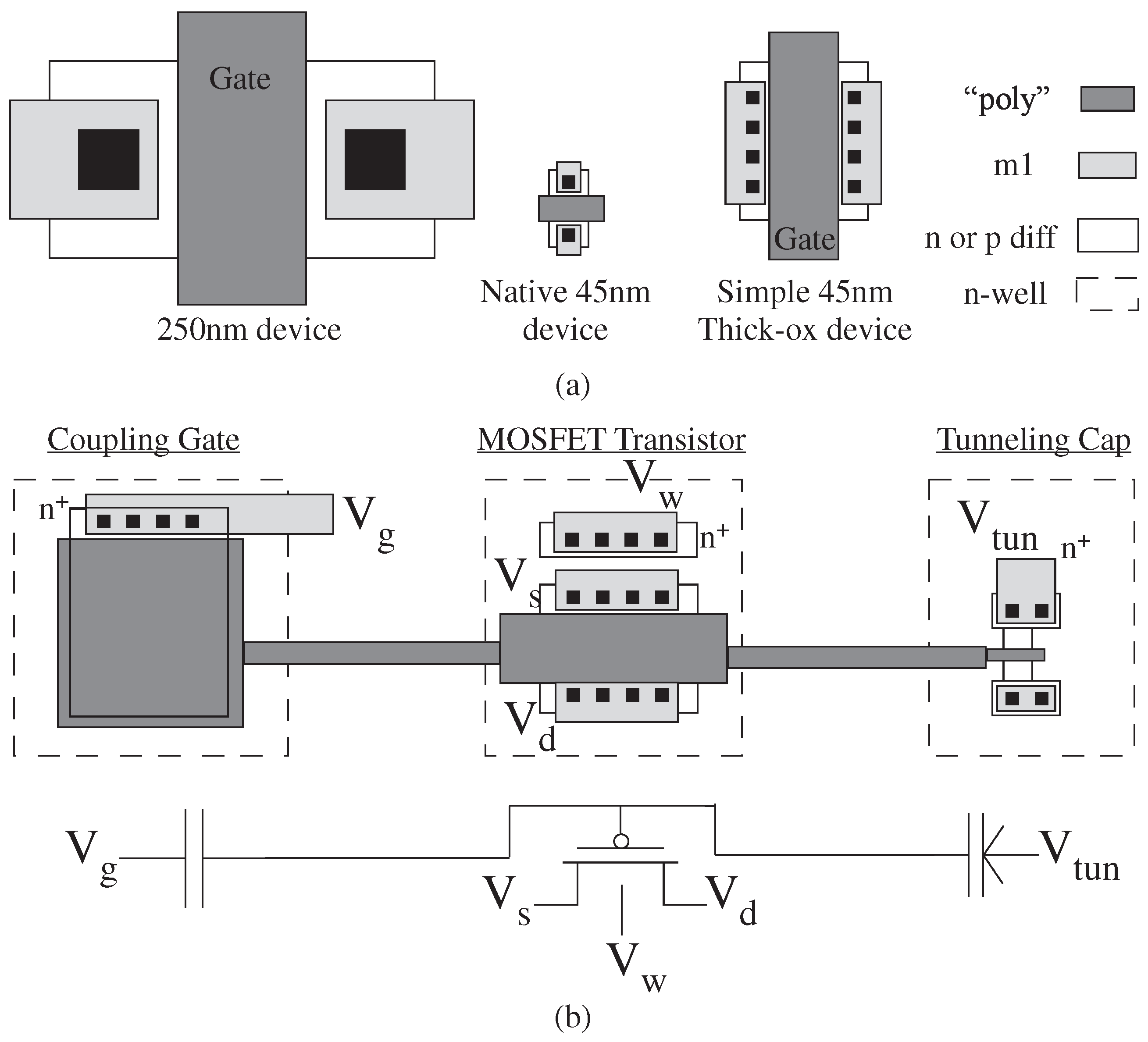
Figure 3a shows scaled pictures of different transistor sizes; the thicker insulator device for 45 nm process, although having a gate similar to a 250 nm process enabling long-term storage, has drain-source parasitic capacitance similar to a 45 nm process. Minimizing these parasitics is critical for frequency performance for any implementation, as well as important for keeping routing fabric as small as possible. Decreasing the entire size to a typical 45 nm device with a thicker insulator, typical of EEPROM type devices, is possible.
Figure 3b shows the top level (e.g., layout) generic view of a single-poly FG device. Practical devices have additional improvements; some are process dependent. This core structure, as shown, is used in every FG test structure since it characterizes baseline performance of these devices, starting from its initial introduction [
22]. The structure is similar to the double-poly structure shown in
Figure 2 of [
8]. These devices do not put the gate coupling directly above the gate electrode, as in EEPROM devices, but rather the gate is brought out for
analog control of the resulting device. One should never have contacts to the gate electrode; contacts can significantly increase the resulting gate leakage.
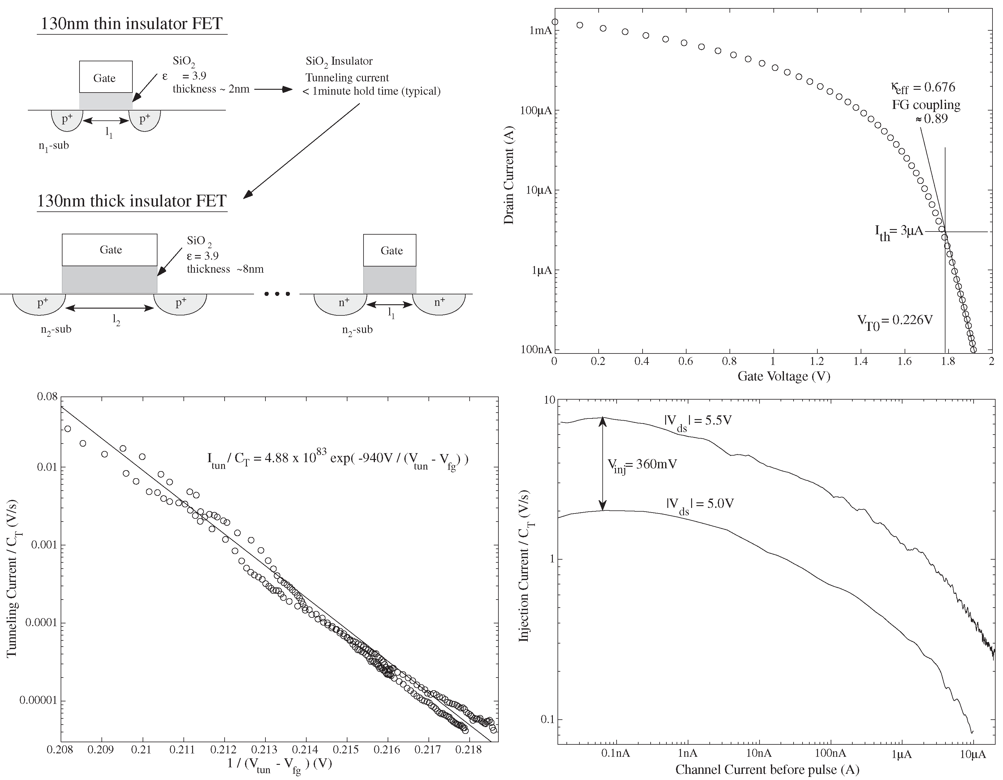
2.1. 130 nm FET Measurements
Figure 4 illustrates moving FG devices from 350 nm to smaller line width processes with SiO
gate insulator; this example shows data from a 130 nm CMOS process. FG devices are built from the larger insulator thickness, available in all processes smaller than 350 nm CMOS; the smaller insulator thickness allows significant tunneling current even with no voltage across the insulator. The insulator thickness is typically the size of a 350 nm CMOS insulator thickness (≈7 nm); we expect (and measure) similar (if not better) FG charge storage seen in the 350 nm processes [
9].
Figure 4 shows measurements of typical channel current versus gate voltage, typical tunneling current versus gate voltage measured through channel current, and typical injection current versus gate voltage (measured through channel current) and drain voltage. These measurements show typical behavior seen in 350 nm devices (e.g.,
Figure 2).
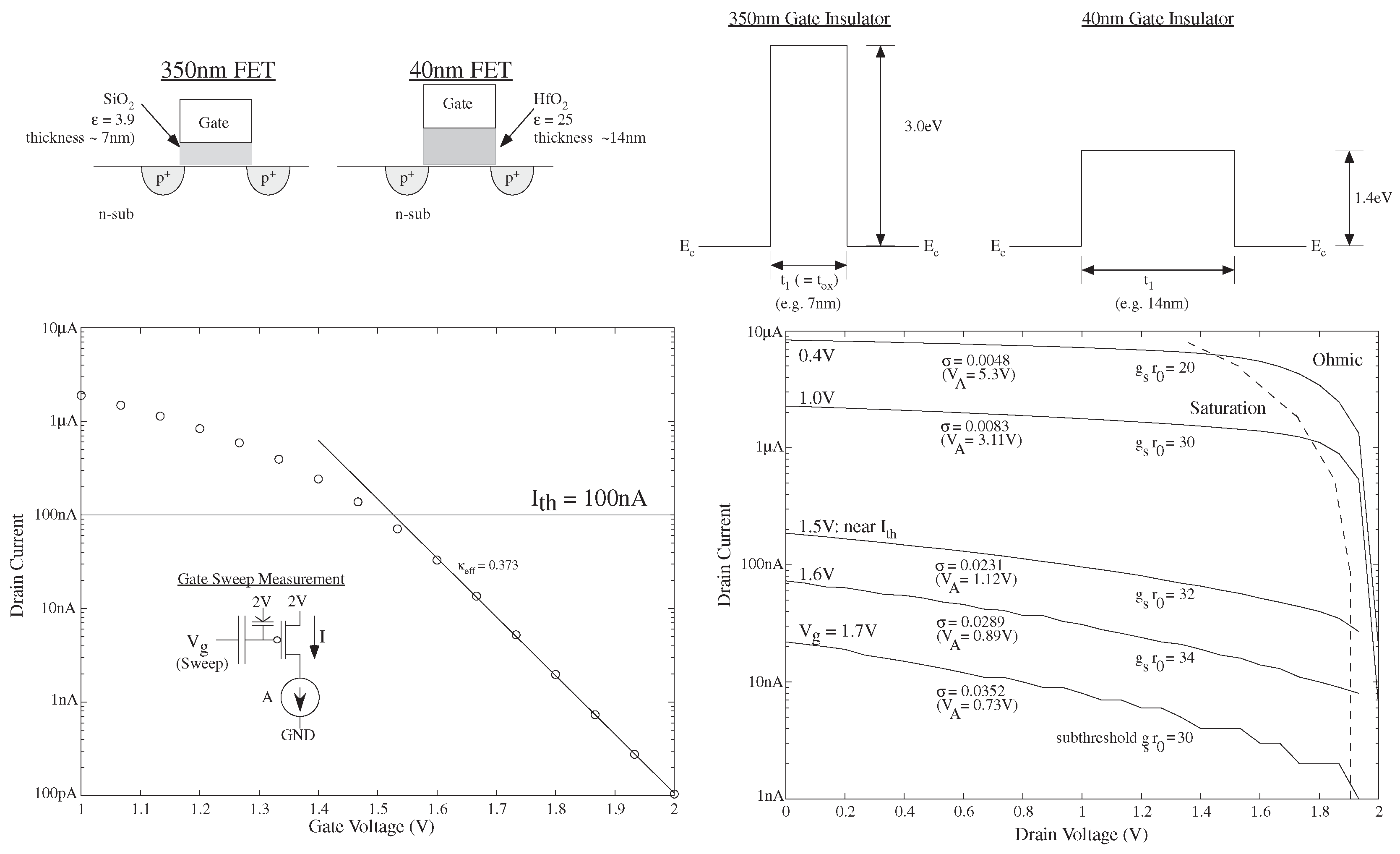
2.2. 40 nm FG Devices
At 45 nm/40 nm (from 65 nm), one sees a major change in the resulting MOSFET device, in that we have a change in gate insulator from the time-tested SiO
to HfO
to reduce gate leakage in the thin insulator devices.
Figure 5 shows a comparison of 350 nm to 40 nm FG devices, with the opportunities and changes due to a change in the gate insulator. The first question is whether these new FG devices hold charge, at least sufficiently long for testing our systems. In addition, do we get sufficiently long hold-times to expect anything close to 10 year lifetime results? Measurements to date have shown FG devices that hold charge over days with negligible change in the stored charge. To understand the effect, one looks at the square barriers between the 350 nm and 40 nm devices in
Figure 5. The change in insulators do enable a thicker insulator but with a smaller barrier potential (1.4 eV [
23] versus 3.0 eV [
20]); therefore, for a square barrier we would expect lower leakage than the 350 nm device. The leakage for the typical MOSFET at 40 nm, due to the larger insulator being lower than the leakage for a 90 nm/130 nm device. The FG device uses a thicker insulator to enable long (i.e., 10 year) charge storage lifetimes; this insulator thickness results in leakage levels expected in a 350 nm device.
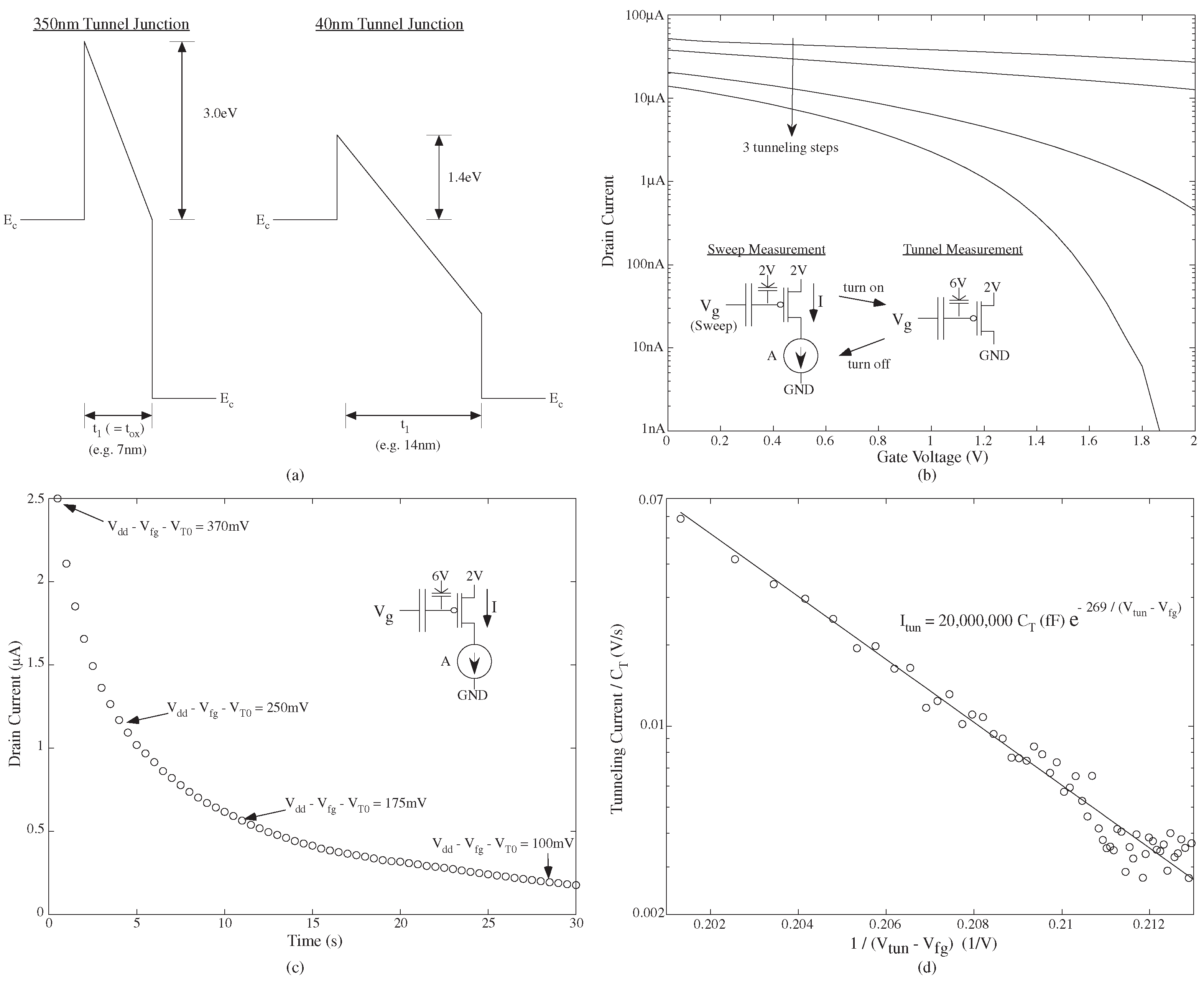
Figure 6 shows the concept and measurement of electron tunneling through the HfO
gate insulator. In both cases, electron tunneling is described by classic Fowler–Nordheim tunneling. The modified 40 nm FG FET insulator results in higher electron tunneling current because of the smaller barrier to Si (1.4 eV) versus the classic SiO
to Si barrier (3.0 eV). In regressing the tunneling data, we can assume for the region used that we are in a typical MOSFET region, since these are designed to handle higher voltages. For our above-threshold current measurement versus time, we can take our model of current–voltage relationship (verified by data to be reasonable) as
where threshold current,
I, as
,
, and we extracted
I as 100 nA from our data on this particular device. From these measurements of
V, we can extract tunneling by writing Kirchoff’s current law at the FG as
The resulting formulation allows us to take a numerical derivative to see the resulting tunneling current, enabling the plot in
Figure 6 and resulting curve fit of (
3).
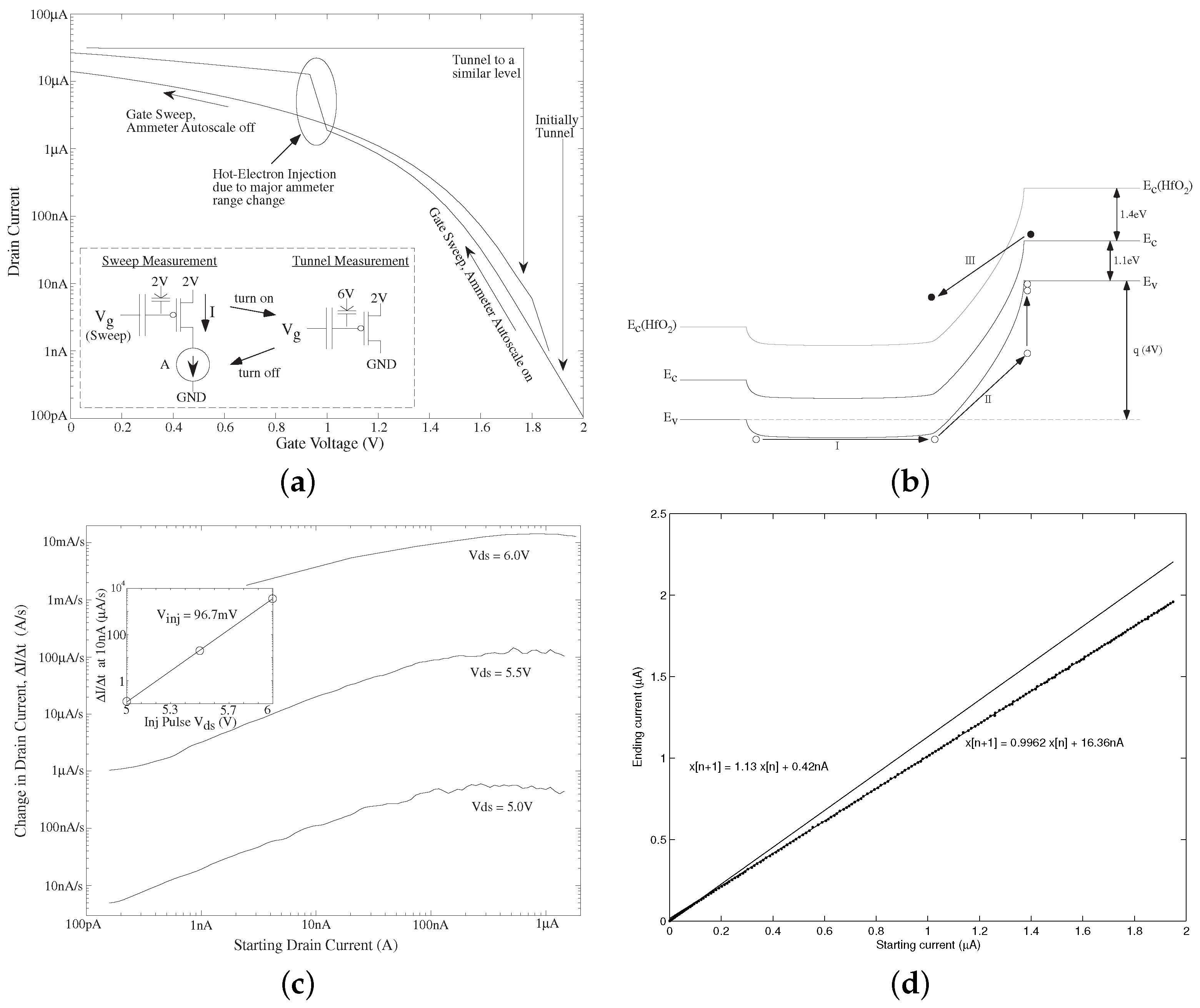
Figure 7 shows the discussion for the hot-electron injection process. The lower energy barrier between HfO
impacts channel hot-electron injection by reducing the barrier for electrons injecting into the insulator.
Figure 7b shows the band diagram and the three steps required for hot-electron injection. The first step requires movement of holes through the channel region. The second step requires movement of holes through the drain-to-channel region, resulting in high energy carriers impact ionization, creating a source of electrons for the conduction band. The third step requires movement of electrons back through the drain-to-channel region, resulting in high-energy electrons that can surmount the insulator interface. For SiO
barriers, a wide range of the effects were limited by hole impact ionization, and we expect in these processes that the correlation will be far stronger. We expect that we will need similar voltages for injection across processes.
Qualitatively, the results are similar to hot-electron injection in larger MOS devices.
Figure 7 shows a typical MOSFET injection characterization to determine parameters for FG programming [
10].
Figure 7d shows an incremental increase due to injection. Often in programming algorithms, we make use of an effective linear difference equation(s) for early steps in reaching target value [
10]. These approaches allow using simple fixed point functions for calculating FG injection pulses to reach an analog FG target.
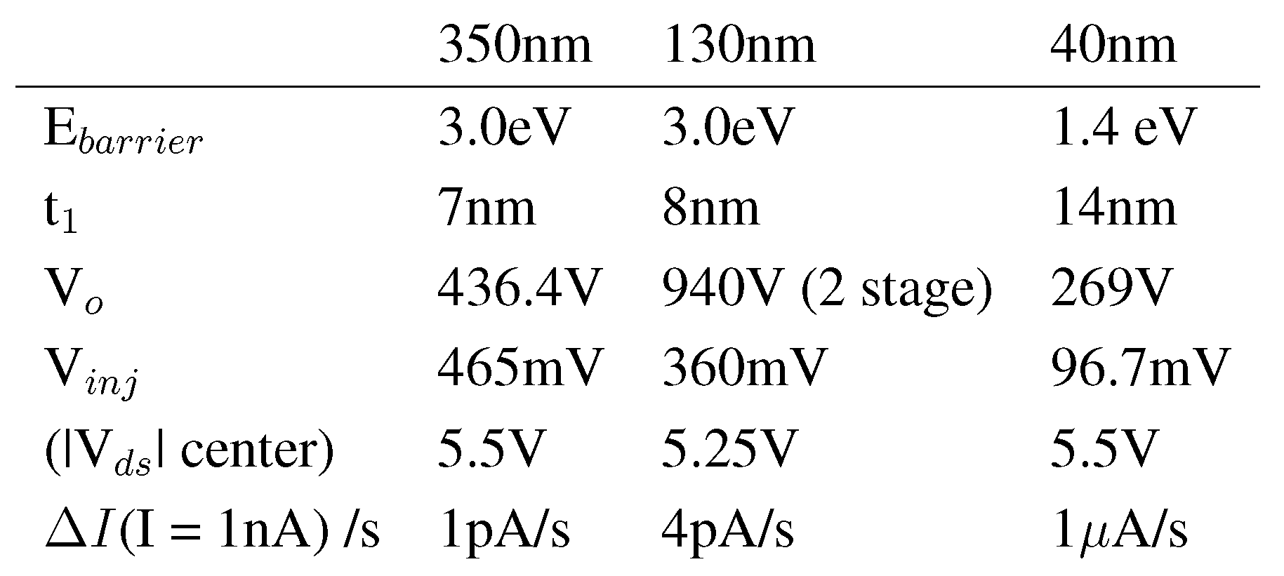
2.3. FG Scaling Discussion
Figure 8 shows a progression in efficiency between the three processes for these approaches in terms of required applied voltages. The change in insulator, with its change in barrier height (3.0 eV to 1.4 eV for HfO
), makes 40 nm significantly more efficient in FG writing capability, while still enabling 10 year lifetimes. For tunneling, we get a smaller
V due to the lower starting barrier, and the quantity
remains nearly constant (less than 6% change) between 350 nm and 40 nm devices. For injection, we get a significantly higher injection current and sharper slope (as seen by
V), as a combination of efficiency and higher substrate doping. We expect similar behavior scaling down to 14 nm devices give the similar insulator structure.
Although scaling of tunneling physics is straightforward, scaling of hot-electron injection physics for these pFET devices should receive additional discussion. Hot-electron injection in pFET devices, operating at sub threshold and near threshold currents, are influenced mostly in the increased substrate doping allowed by the stronger insulator capacitor coupling, as well as the different Si-insulator barrier height. The substrate doping does not increase as fast because of the doping profile used for thicker insulator devices; when this layer is removed, one expects higher electric fields and lower impact-ionization and hot-electron injection voltages. Impact ionization always occurs significantly before any further device breakdown effects. We have two regions to consider, the hot-hole transport and resulting impact ionization that creates the resulting conduction band electrons, and the hot-electron transport and resulting electron injection efficiency.
The restoring force for the electron and hole high-field transport is primarily optical phonons, where first the carrier needs to gain more energy per unit distance than the optical phonon restoring force (E
/
λ) typically requiring a starting distance (z
) for an increasing potential, and then the average carrier trajectory includes field gained energy minus this required starting energy. The resulting distribution function around this average trajectory is a local convolution of Gaussian functions, the eigenfunction of a linear diffusion equation (e.g., heat equation). We have discussed these fundamental transport details elsewhere [
21].
Electrons in an electric field will gain energy faster than holes in an electric field, as characterized by their typical mean free length for an optical phonon collision of energy
E (≈63 meV), where electrons (
) are approximately 6.5 nm [
21], and holes (
) are approximately 4.2 nm [
24]. Although impact ionization can occur for an electron or hole with energy of 1.1 eV, requiring carriers to exceed this barrier, electron impact ionization is known to be an efficient process for electron energies above 2.3 eV [
21,
25], and hole impact ionization is known to be an efficient process for hole energies above 3.0 eV [
24]. The resulting created electrons, sometimes starting with additional energy because of the impact ionization process, begin around the highest field region, gaining energy as they accelerate to get over the 3.0 eV (Si-SiO
) or 1.4 eV (Si-HfO
) barrier.
The 3.0 eV barrier level for significant hole impact ionization would be the primary limit for the hot-election injection process when using a Si-SiO barrier (3.0 eV) given the significant difference between and , although some functional dependance is still possible. The 2.3 eV level for hot-electron impact ionization means we will get some significant loss of electrons before reaching the Si-SiO barrier (3.0 eV), while we have negligible loss of electrons before reaching the Si-HfO barrier (1.4 eV), resulting in significantly higher injection current. For the Si-HfO barrier, the electron dynamics can almost be approximated by a constant factor, and approximation often desired (but not physically correct) between injection and impact ionization currents.
3. Scaling of an FG MOSFET Used in an Array of Switches
Because we have proven that FG devices are functional throughout a wide range of CMOS IC processes, we now transition to looking at the scaling properties of an FG MOSFET acting as one of the multiple switches, say, in a small crossbar array (e.g., [
7,
17]). The operating speeds of an FPAA array is, to first order, limited by the FG MOSFET switch. We will analyze the high frequency behavior of a switch in an array of switches (e.g., routing fabric). For this analysis, a programmed switch is at one of two cases, when the switch is
off and when the switch is
on. A programmed FG voltage can be set at significantly higher or lower voltages than the power supply range. Our discussions focus on nFET and pFET devices; these dynamics are effectively interchangeable with slight changes in parameters.
3.1. Off-Switch Behavior
For the off switch case, we start with the channel in accumulation. Because the switch value can be programmed outside the power supply, a slightly positive value (above V) will guarantee the device stays in accumulation for all applied voltages including the GHz frequencies that we are considering in this discussion. In accumulation, we have no appreciable depletion capacitance, and, therefore, the capacitance between the floating-gate terminal and the substrate is the oxide (or insulator 0 capacitance ( W L ). The effective conductance between source and drain is effectively zero, being the conductance of two reverse-biased diodes. Gate length has little to do with the off case (other than total gate capacitance) in accumulation.
With the zero conductance between source and drain, any potential communication between switches must happen through capacitive coupling. The gate to source-drain junction capacitance, C, is the biggest issue in terms of signal feedthrough, which scales proportionally to other device properties. Minimizing C decreases the amount of capacitive signal feedthrough feedthrough, which could be further decreased by opening up drain-source regions (avoiding some of the self-aligned device). C and C p-n capacitors connected to signal ground (actually V). Therefore, the frequency-indpendant coupling gain from source to drain voltage would be the resulting capacitive divider network as C/(C C), where C is the total capacitance of the floating-gate node. Both terms result in a coupling less than ; with multiple switches in series, this value is nearly negligible. In a switch matrix, the resulting load capacitance is the sum of all of the capacitors on the line, further decreasing this effect. Furthermore, this effect is negligible in 350 nm FPAA devices at low frequencies, with no significant coupling measured whether in characterization or in applications.
3.2. On-Switch Conductance Behavior
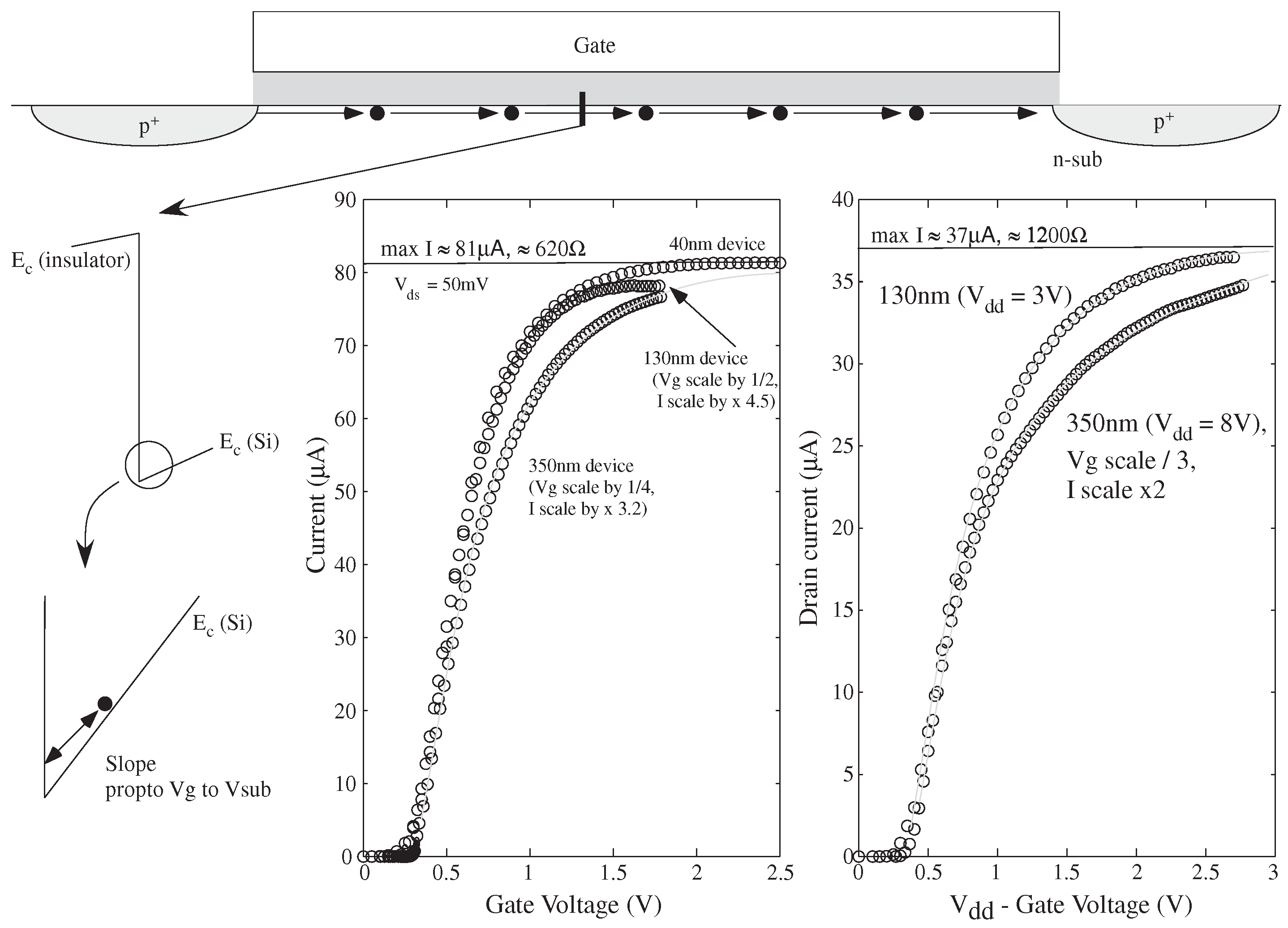
For the on switch case, we are primarily concerned with the frequency response through the particular device. The MOSFET channel is biased far above threshold behavior, operating in the ohmic regime. The FG voltage is not constrained between the power supply rails, allowing the transistor to its maximum conductance point, the point for high gate voltage where the source-to-drain conductance of channel is approximately independent of gate voltage. This maximum conductance, or R, is roughly independent of process minimum channel length, where the conductance is set by velocity saturation of electrons/holes for the MOSFET channel. For a device with equal width and length, the nFET saturates around 3 kΩ and pFET near 6 kΩ.
Figure 9 presents the discussion for this maximum conductance, where an increase in gate voltage increases the number of collisions with Si–insulator barrier while carriers effectively move from source to drain voltage. An
on MOSFET switch typically would have a small voltage between the source (
V) and drain (
V) voltages, resulting in the MOSFET modeling
where
μ is the carrier mobility in the channel,
is the insulator capacitance per unit area (
),
κ is the capacitive divider between
C and the total capacitance in the channel,
V is the threshold voltage, W and l are the width and length of the MOSFET device,
Q and
Q are the channel charge at the source and drain edges of the channel region, respectively. The measurement in
Figure 9 uses
V = 0 V,
V = 50 mV for continuously ohmic operation, while sweeping
V over a wide voltage range. In this setup,
V is set to the substrate (so
V = 0); and pFET are measured down from their substrate held at
V (different for each technology). One would expect a conductance (
G) that linearly increases, after
V, with
V, as
Figure 9 shows measured data illustrating this initial linear behavior, as well as deviations from it leading towards conductance saturation.
The modeling for conductance saturation investigates the change of
μ with gate voltage; other terms remain nearly constant.
Figure 9 shows that, although we draw carriers (e.g., electrons) moving in a straight line path through the channel from
V to
V, we have a field in the orthogonal direction (gate direction) that pulls these carriers towards the gate region. These carriers get pulled into the Si-insulator barrier, elastically colliding and reversing direction towards the substrate until the electric field of the channel brings the carriers back towards equilibrium. From (
8), the electric field at the Si-insulator barrier
The electric field in
S will decrease moving into the depletion region. A constant electric field (linear change in potential) is expected at the boundary layer right at the Si-insulator boundary. The additional elastic collisions will decrease the resulting carrier mobility,
μ,
where
τ is the mean free time due to collisions,
is the carrier effective mass,
is the mean free time due to typical restoration forces in the channel, such as acoustic phonons, elastic scattering mechanisms, as well as any effects due to some optical phonon behavior, and
is the collision component due to average elastic collisions with the Si–insulator barrier. Transit time would be the ratio of average distance traveled over the average velocity of carriers. The energy of the carriers through the channel is never high, roughly at the typical kT =
q U average energy for a Fermi distribution (energy less than Fermi level), for an average distance traveled (due to electric field) as
U/
. Velocity of carriers at lower
is proportional to
. Velocity of carriers at higher
approaches velocity saturation,
v; in this region, we get
For increasing
V, the transport progresses starting in the region with a constant
, resulting in classical linear increase in conductance, to the region where
τ is decreasing due to elastic collisions, resulting in a sub linear increase in conductance, to the region where
τ is dominated by
with large
. In this final region, where the conductance saturates at
G, the current is expressed as:
where
G is not a function of typical device parameters, except for drawn transistor width and length.
G is not a function of the insulator thickness.
Figure 9 shows 350 nm, 130 nm and 40 nm nFET or pFET device measurements illustrating the conductance saturation in each case.
3.3. On-Switch Capacitance Behavior
The other side of the question is the resulting capacitance to set the resulting time constant. For example, we can make wider MOSFET switches, decreasing the resulting channel resistance, but increasing the resulting capacitance found in a dense array of FG devices. Switch capacitance is primarily due to source-drain junctions, C and C, as well as a small capacitance through the FET gate oxide, through the resulting capacitive network to other potentials. We identify the resulting capacitance as C. The relative size of these capacitances typically scales quadratically with scaling of process line width.
The design of such an array must discuss whether to have the well connected to signal GND, which would be a solid GND even for RF frequencies, or have a high-impedance connection. A useful high-impedance to each switch requires that each switch be placed in a separate isolated well device, as well as having a high resistance connection to the resulting well terminal.
Therefore, for a single switch, we see minimal additional coupling effects through the switch. We expect there will be some effect of the RC effect in the channel (usually modeled by a resistor and inductor) of course, around f (max) due to maximum conductance. The low frequency modeling directly applies to our modeling approaches.
4. FPAA Capacitance Measurement, Modeling, and Architecture Tradeoffs
Having working FG devices as well as modeling of individual switches, we move towards modeling the frequency response of an FPAA fabric, justifying
Figure 1b.
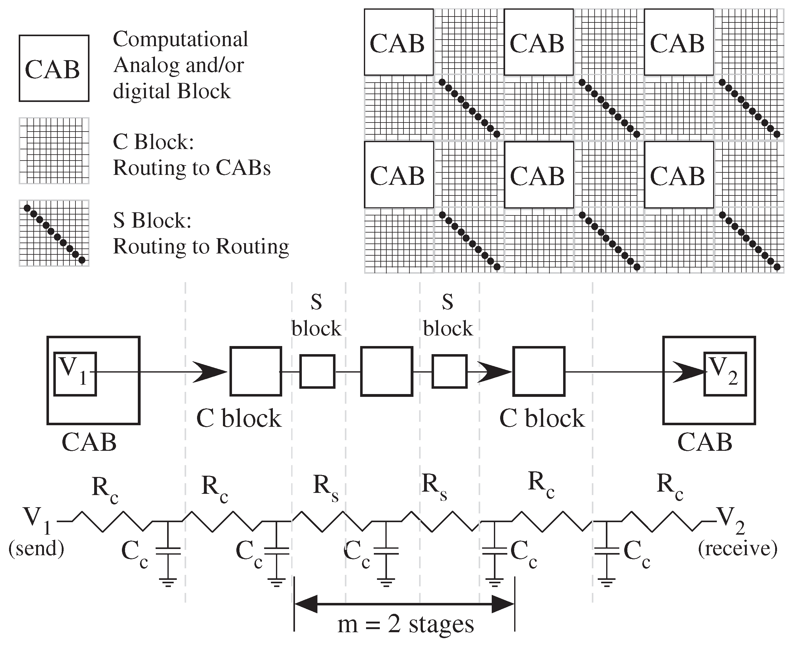
Figure 10 shows the basic Manhattan based routing structure used for our SoC FPAA device (i.e., [
7]). The approach includes a compartment for a Computational Analog Block (CAB) or a Computational Logic Block (CLB), includes two Connection (
C) blocks to connect these devices, and includes one routing Switch (
S) block. Using the Manhattan style routing enables direct interactions with existing tool flows ([
26]). We still hold that the routing fabric in this architecture is both useful for computation as well as switching, particularly for local CAB/CLB routing as well as in the ‘
C block routing. Other FPAA architectures show similar approaches and tradeoffs, although this architecture mades these issues more explicit.
From a classical FPGA approach, one considers the capability of the device to be solely in its components (CLBs, specialized blocks), and the routing fabric is simply a mechanism to interconnect these components. Minimizing the effect of the routing fabric reduces, from a circuit perspective, dead weight that can only degrade the circuit. This approach requires minimizing the number of switches, each of which adds resistance, as well as minimizing the resulting capacitance of the routing. The routing infrastructure can effectively be modeled as a distributed RC line. The architecture looks at the relationship of the resulting switch resistances, as well as other circuit uses of the FG switch devices as a function of the number of CAB inputs and number of tracks, as well as the typical number of switches needed for a connection.
4.1. SoC FPAA Routing Fabric Characterization and Computation
The SoC FPAA [
7] enables programming experiments that characterize the fundamental properties of the configurable fabric by experimental measurements on the configurable routing fabric.
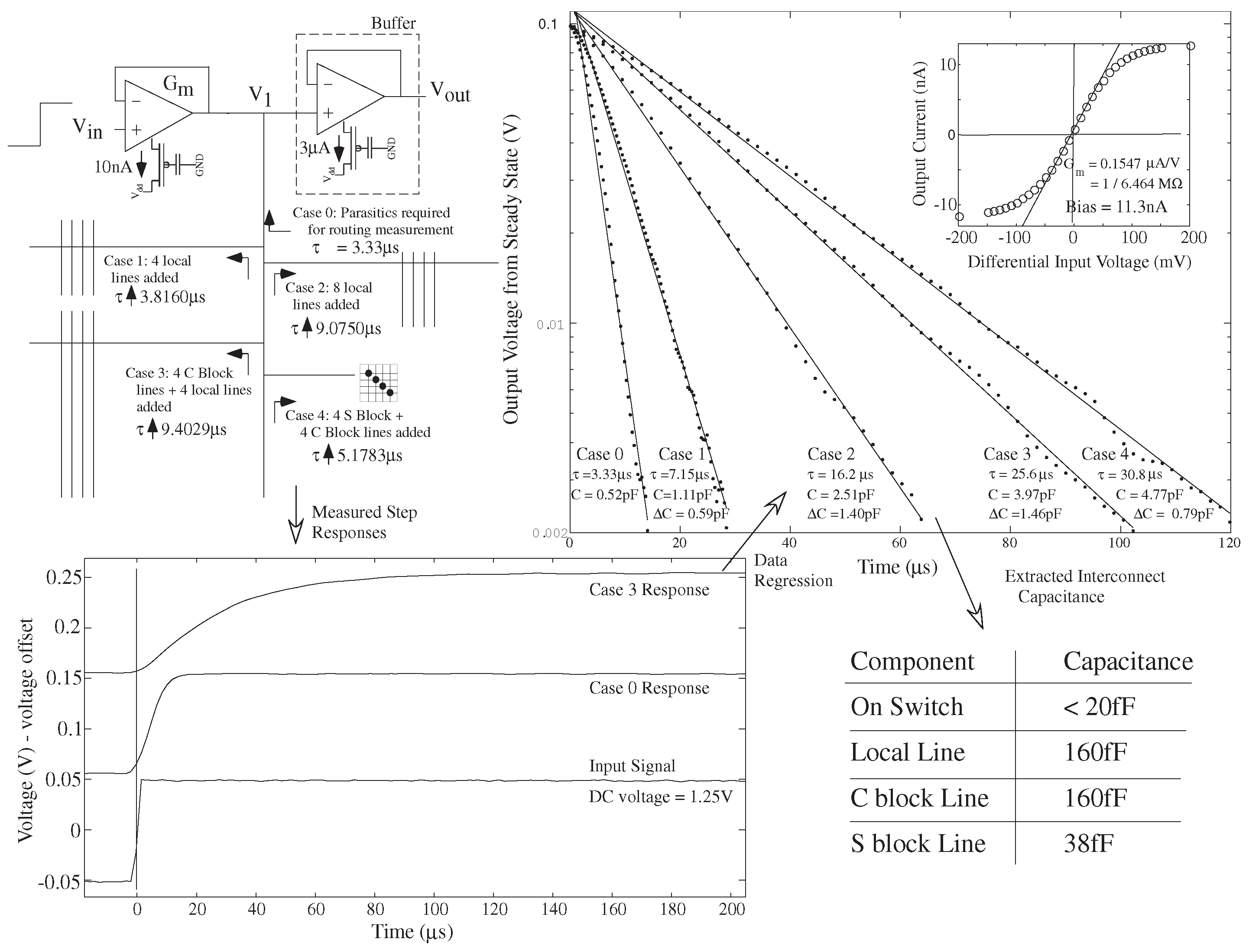
Figure 11 illustrates compiling (and measuring) two circuits to characterize precisely the behavior of these circuits, including load capacitance of the fabric itself. This FPAA structure facilitates the direct characterization of the resulting capacitance, coupled with the resistance of an on-switch,
R. One can directly predict delays along each of these lines. Every experiment uses the same voltage biasing, fixing the capacitance of p-n junction devices throughout this experiment. The resulting measurements give a measurement of the resulting routing capacitance, as well as enables, through the routing fabric, a range of tunable capacitor blocks. Precise measurement of routing capacitances enables tuning, through programming switches, for precise capacitances where needed for matching. Matching of capacitances and programmability of current sources by FG techniques dramatically reduces the effect of mismatch in small cell sizes.
4.2. Architecture Tradeoffs for FPAA Switch Fabric
Next, we use our FG switch and network modeling to look at speed through routing fabric (
Figure 10) like the SoC FPAA [
7]. The architecture choices look at the relationship of the resulting switch electrical properties, as a function of the number of CAB inputs and number of tracks (
n), as well as the typical number of switches needed for a connection (
m).
Figure 10 shows a case when
m = 2. We have routing in and out of the CABs: a connection in the CAB and a connection in the first
C block. In this analysis, every route starts with these four connections, and might require more routes through additional
S and
C blocks. We consider a point-to-point communication scheme; one can extend this modeling to other connections, expecting similar scaling rules. The pure switch routing approach is often the worst case situation for capability and computation speed through a routing fabric; the situation often simplifies when using routing for computation (e.g., classifier in [
7]).
Figure 12 illustrates one set of tradeoffs as well as a summary of the key parameters of switch conductance and capacitances. We consider that capacitance as
C, which is due to multiple (
n) source-drain junction capacitances (
C), or
. An approximation of the time constant (
τ) is computed to analyze the fabric communication frequency (=
). The first-order approximation for
τ is the product of all resistances along the line times all capacitance along the line. This formulation is an overestimation of the resulting time constant, typical for an infinite (diffusive) RC line. The total resistance along the line is
; four switches to get signals on and off a
C line with all other switches in
S block. We allow for the
S switch to be larger (in
W) than the
C switch by a factor
A, resulting in
. Active devices in the
S switch elements reducing the resistive effect when required. The total capacitance along the line is
; larger
S block switches have proportionally more capacitance. As a result,
τ is
for moderate levels of
m. Typically
and
. One would typically design
to be significantly less than 1; the optimum point seems to be
. We would simultaneously want to minimize
n and
m. Minimizing
n enables higher frequency, as well as lower power consumption. Minimizing
m decreasing the resistance through the path.
Finally, we show evidence for the quadratic scaling law given in
Figure 1b. At this optimal point,
By including the dependancies of
R and
, where
C is
C per unit area, we get
resulting in
We expect a quadratic scaling of frequency with channel length for the same architecture structure, as seen in
Figure 1b. We notice the size does not depend upon
W, giving the designer freedom to choose W based on other constraints. The substrate doping does not change much by process starting in 130 nm process, being effectively degenerately doped. Furthermore, higher insulator FETs often use a slightly lower substrate doping for their devices. One might have seen an issue if we started FPAA development using 2
m CMOS.
The architecture sets the frequency response.
Figure 12 shows tradeoffs for a 45 nm IC CMOS process.
Figure 12b solving for frequency boundary for 4 GHz frequency, and
Figure 12c solving for frequency boundary for 500 MHz frequency. This process enables 4 GHz signal frequency through both routing fabric and components.


