1. Introduction
The ever increasing data crunch in wireless communication necessitates the means to increase the data rate with spectral efficiency. There are three main approaches to increasing the data rate in wireless communication: high-order modulation schemes (e.g., 64 QAM (Quadrature Amplitude Modulation), 128 QAM, and 256 QAM), high carrier frequency with large fractional bandwidth, and carrier aggregation (CA). The high-order modulation format is able to offer faster data rates and a higher level of spectral efficiency, but practically, modulation format is dictated by the link-budget, signal-to-noise ratio (SNR), and transceiver performance. High carrier frequency (e.g, millimeter-wave bands from 30 GHz to 300 GHz) is beneficial because signal bandwidth is a certain fraction of carrier frequency, and thus higher carrier frequency leads to large signal bandwidth. However, hostile channel characteristics at millimeter-wave bands reduce service coverage and impair communication performance [
1].
CA raises the bandwidth and capacity by combining two or more adjacent or non-adjacent RF channels [
2]. CA is also the technical solution to overcome spectrum fragmentation, and can be applied to a wide variety of spectrum scenarios [
3]. CA has been adopted by the Long-Term Evolution (LTE) standard for cellular systems, and is being extended to Licensed-Assisted Access (LAA) and LTE in Unlicensed spectrum (LTE-U). In addition, CA will be one of the key features to enable future 5 G wireless systems.
A plethora of wireless standards exist in the radio frequency regime, and the number of wireless devices is increasing rapidly. Reception of wireless signals is becoming more challenging due to spectrum crowding and reduced channel capacity under the harsh wireless environment. Low noise performance is a must to improve the SNR of the reception signal at the sensitivity level. On the other hand, high linearity of the receiver is the capacity to handle large signal interferences and jammers with the simultaneous reception of small desired signals.
These considerations call for new innovations on several fronts, from the circuit to the architectural level. In this paper, we propose a high-performance receiver architecture supporting legacy single-carrier operation, inter-band carrier aggregation, and intra-band carrier aggregation. The proposed architecture can be considered a single-input, and multi-output (SIMO) receiver, and two contrasting requirements—noise and linearity—which set the dynamic range performance of RFICs (Radio Frequency Integrated Circuits) are satisfied simultaneously. We demonstrate that the proposed architecture does not sacrifice performance in single-carrier operation, and no additional matching element is required. Comparative performance in different operation modes are elaborated.
This paper is organized as follows. The system description of the proposed receiver architecture is discussed in
Section 2. Several low noise amplifier (LNA) topologies suitable for receiver (RX) carrier aggregation are presented, and are evaluated with the proposed receiver architecture in
Section 3. Concluding remarks are given in
Section 4.
2. Receiver Architecture
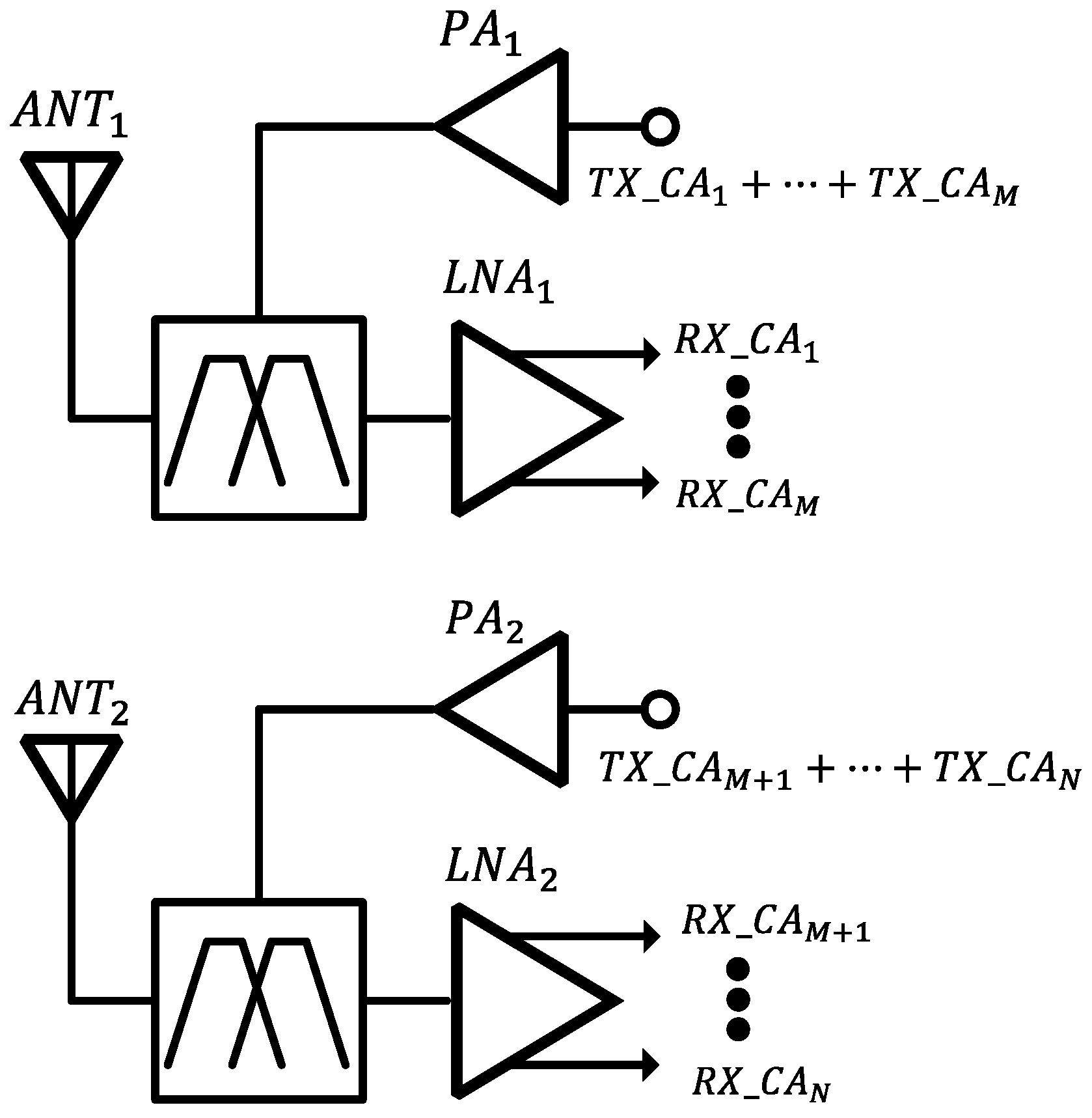
Figure 1 shows the concurrent transceiver architecture supporting N carriers. When RF carriers belong to the same band, it is called intra-band aggregation. If they come from different bands, then it is named inter-band aggregation. In the former case, they are defined as contiguous or non-contiguous when the channels are adjacent to each other or not, respectively. Support of N carriers does not necessarily mean that N transceivers are required. For instance, ideal software defined radio envisioned by Mitola [
4] can support concurrent operation of N carriers with only a single transceiver. However, existing transceivers—specifically receivers in this paper—are limited in their RF operation frequency (RF bandwidth) as well as intermediate frequency (IF) (baseband bandwidth). Therefore, we consider a generic case where N transceivers are supporting N carriers simultaneously.
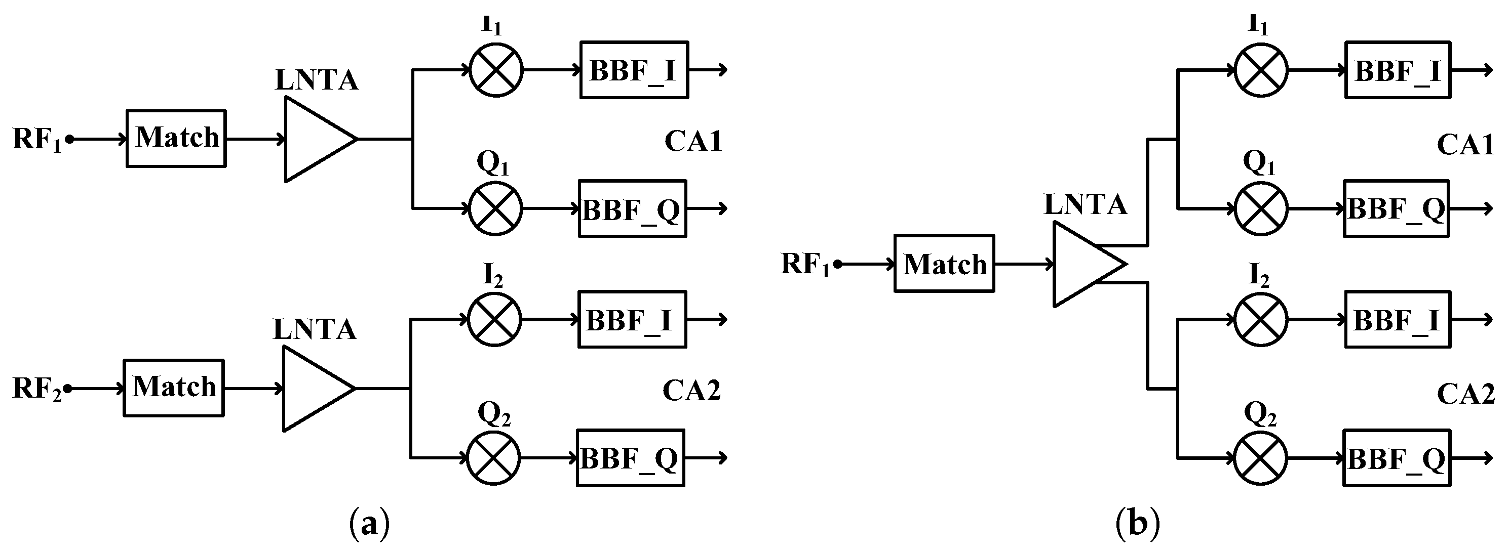
CA allows for the full utilization of fragmented spectrum, and different types of CA come from the location of the fragmented spectrum to be combined. The design of the digital baseband is almost invariant to the different CA types. On the other hand, design complexity of radio-frequency transceiver depends heavily on the CA types [
3]. Without losing generality,
Figure 2 shows two different implementations of the receiver supporting two CA carriers.
Figure 2a supports two inter-band carrier signals, and parallel signal paths are optimized for different frequency bands. For instance, RF1 and RF2 denotes the carriers at band 2 (1930–1990 MHz) and band 12 (729–746 MHz), respectively. Due to the limited RF and IF bandwidth of the circuitry, a single signal path receiver that supports both band 2 and band 12 simultaneously is not easily feasible, and we thus have to adopt separate signal paths.
Figure 2b is the embodiment of a two CA receiver with the support of intra-band CA. Due to the limited IF spectrum coverage with the baseband circuits (e.g., variable-gain amplifier, filter, etc.), N (= 2 in
Figure 2) receiver signal paths are required to support both contiguous and non-contiguous intra-band CA.
The RF bandwidth that each signal path can support is mainly dictated by the input matching network (IMN) bandwidth. All the low-noise trans-conductance amplifiers (LNTAs) discussed here are based on the inductor-degenerated common-source stage. The matching network utilizing the
of the main transistor is based on the series RLC resonance circuit, where its quality (
Q) factor is typically larger than 1. Passive voltage amplification due to the matching network is beneficial for the receiver with improved signal-to-noise ratio. On the other hand, the bandwidth is inversely proportional to the
Q-factor (
). For instance, RF1 in
Figure 2a has to support 729–960 MHz to practically receive the signals from band 12 (729–746 MHz) to band 8 (925–960 MHz) with the same receiver path. Then, maximum
Q for RF1 LNTA can be derived as follows.
The limitation in the Q-factor applies to RF2 path as well. Practically, IMN does not possess high Q-factor larger than 5, and this value is acceptable with various 3 GPP (3rd Generation Partnership Project) bands support.
The realization in
Figure 2a is no different from the conventional receiver. Recent advances in receiver architecture opt for the single-
receiver implementation [
5,
6,
7,
8]. With single-gm approach, low-noise active block interfacing the antenna is called a low-noise trans-conductance amplifier, denoted as LNTA in
Figure 2. As the name indicates, LNTA is driving the subsequent stage with a small signal current. Inter-band CA implementation does not alter the characteristics of the LNTA, but the intra-band CA requires the LNTA to deliver multiple outputs.
Section 3 discusses the implementation issue of the LNTA in order to support intra-band CA. Prior to that, in this section, we delve into the architectural issues and concerns to enable a high-performance receiver with large dynamic range.
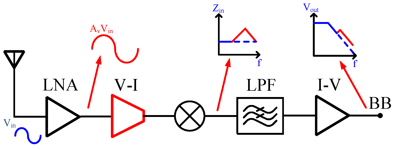
Single- Receiver Architecture
Figure 3 shows the conventional zero-IF receiver architecture with architectural implications. Low-noise amplifier (LNA) is the cascade of V–I (
) and I–V (load) conversion, and Mixer requires separate trans-conductance (
) to drive the passive switching mixer. A low-pass filter with I–V conversion is performed by the single block in either passive (
) or active (trans impedance amplifier—TIA) implementation. The reason for having an LNA is best illustrated with the Friis equation [
9] expressed in Equation (
2). Due to the large gain and low noise figure of the LNA (
and
, respectively), system noise performance is improved with the suppression of subsequent noise coming from mixer and baseband amplifiers. On the other hand, large gain—which is desirable for noise performance—is detrimental to the linearity performance manifested by the cascade
equation given in Equation (
3) [
10]. Large gain due to the front-end amplifies the desired signal as well as large interferences in both in-band and out-of-band. Large interferences either saturate the baseband or worsen the linearity performance of the baseband without proper filtering. Then, low input impedance and the jammer filtering in a broadband IF frequency is highly desirable, both of which are not easily attainable with the current state of the art. On the other hand, the linearity of LNA itself is less of a concern compared to subsequent active stages. Then, we do not adopt the linearization technique, although there have been many efforts to improve the linearity of the LNA [
11,
12,
13].
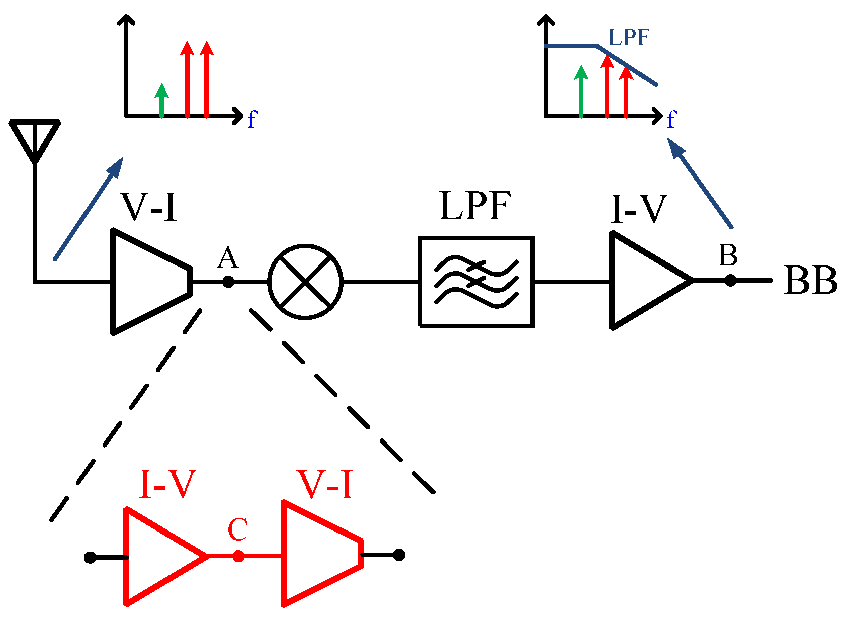
The receiver architecture based on a single low-noise trans-conductance amplifier driving a current-mode passive mixer loaded by a low-impedance trans-impedance closed-loop amplifier has been widely adopted recently due to its beneficial features in terms of noise and linearity [
8].
Figure 4 shows the conceptual diagram of the single-
receiver. I–V conversions of the LNA are eliminated, and thus the remaining V–I conversion is performing as LNTA. Since the output of LNTA is in the current domain, the trans-conductance of the mixer can also be eliminated. Due to the single-
prior to the baseband low-pass filter and I–V conversion, the large voltage swing present in traditional Gilbert-cell and voltage-mode mixers are eliminated. The virtual ground of the TIA minimizes the distortion caused by large in-band and out-of-band interferences. Low-pass filtering performed inside TIA improves the linearity of the receiver system. Due to the low-pass filtering prior to the first I–V conversion in the baseband, the receiver’s robustness to the blocker is improved by the filtering effect. Assume for simplicity that the single blocker is present at the
mth harmonic frequency of LO (Local Oscillator) frequency and the order of the low-pass filter is
n. Then, enhancement in the blocker tolerance (
) is expressed as follows.
where
is the blocker frequency and
is the harmonic rejection ratio of the switching mixer.
Due to the single-
of the receiver, large trans-conductance is essential to maintain low NF and low sensitivity. Inductor-degenerated LNA in common-source configuration is ideal in that respect due to the passive voltage gain coming from the impedance matching network. Moreover, simultaneous noise and power match is achieved by shifting the optimum noise impedance
to the desired value [
14]. Then, CA-supporting LNTA architectures discussed in
Section 3 are considered the extension of the inductor-degenerated LNTA with multi-output support.
3. LNTA Topologies and Simulation Results
In this section, several LNTA topologies are investigated to support both inter-band and intra-band CA. LNTA needs to be in the form of single input and multi-output (SIMO) in order to provide separate signal paths for different carriers. Although two CA carriers are assumed in the implementation, the architecture can be extended to N carriers.
Figure 5 shows the simulated receiver front-end architecture to evaluate different LNTA topologies. LTE band 7 (2620–2690 MHz) is chosen for the implementation and simulation of the receiver. L-section off-chip matching lumped elements are configured with RLC equivalent circuit parameters adopted from Murata Chip S-parameters & Impedance Library. CA-capable LNTA is used as a single-
of the receiver front-end. The main transistor (
) is biased in the sub-threshold region to improve the current efficiency (
). The degradation in the unity-gain frequency (
) due to sub-threshold operation is not a problem per se, since the resonance behavior of the impedance matching network (IMN) cancels out the parasitic effect of the main transistor. The cascode-transistor is half the size of the main transistor, and its gate bias is supplied from the regulated loop to make
of the main transistor at the same potential of the current mirror transistor’s
. A conventional single input, single output (SISO) LNTA is designed for band 7, and is simulated with the test-bench without CA. The gain of the single-carrier receiver front-end as a reference is set at 56.6 dB. NF and current consumption of the single-carrier receiver is 1.33 dB and 7.4 mA, respectively.
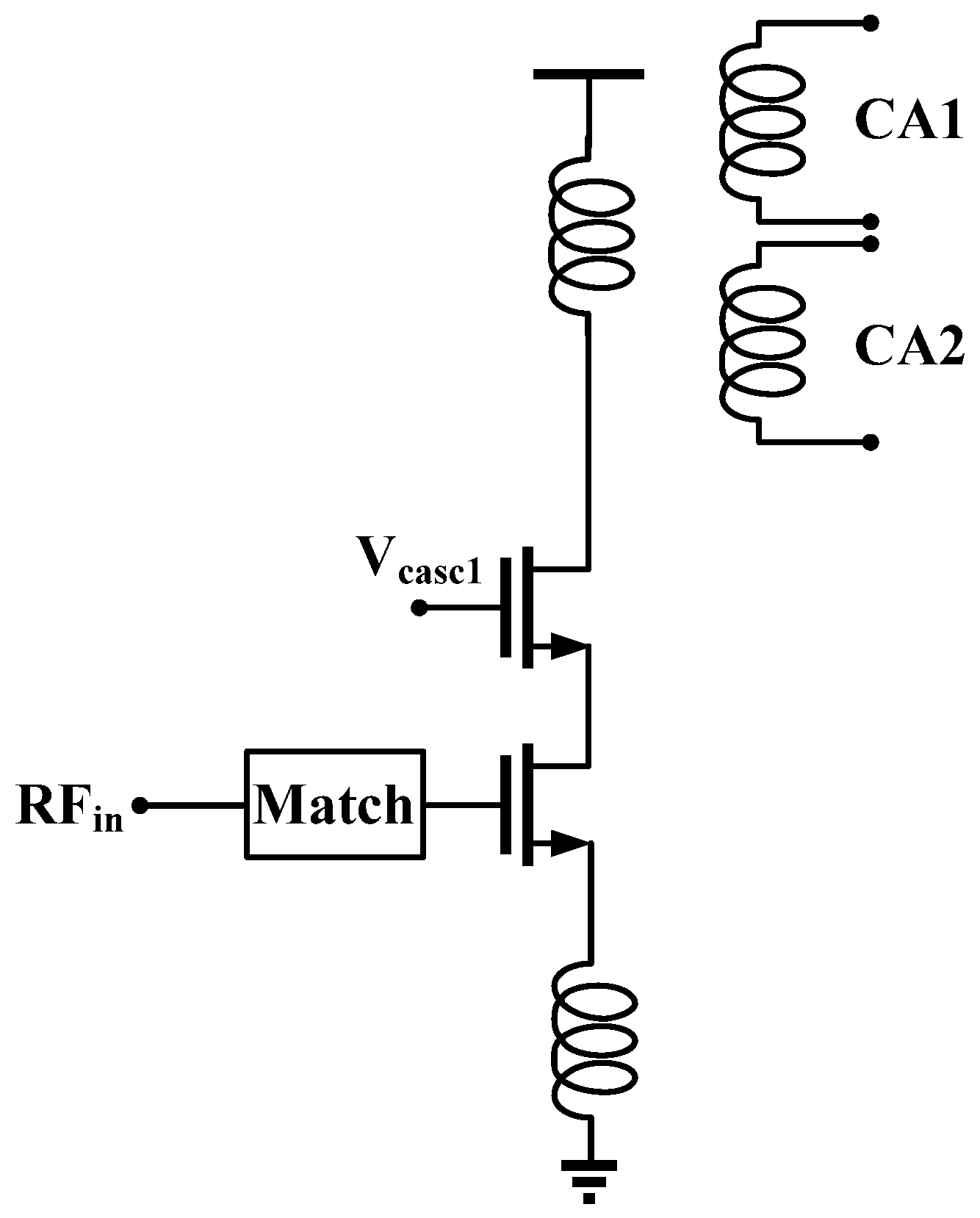
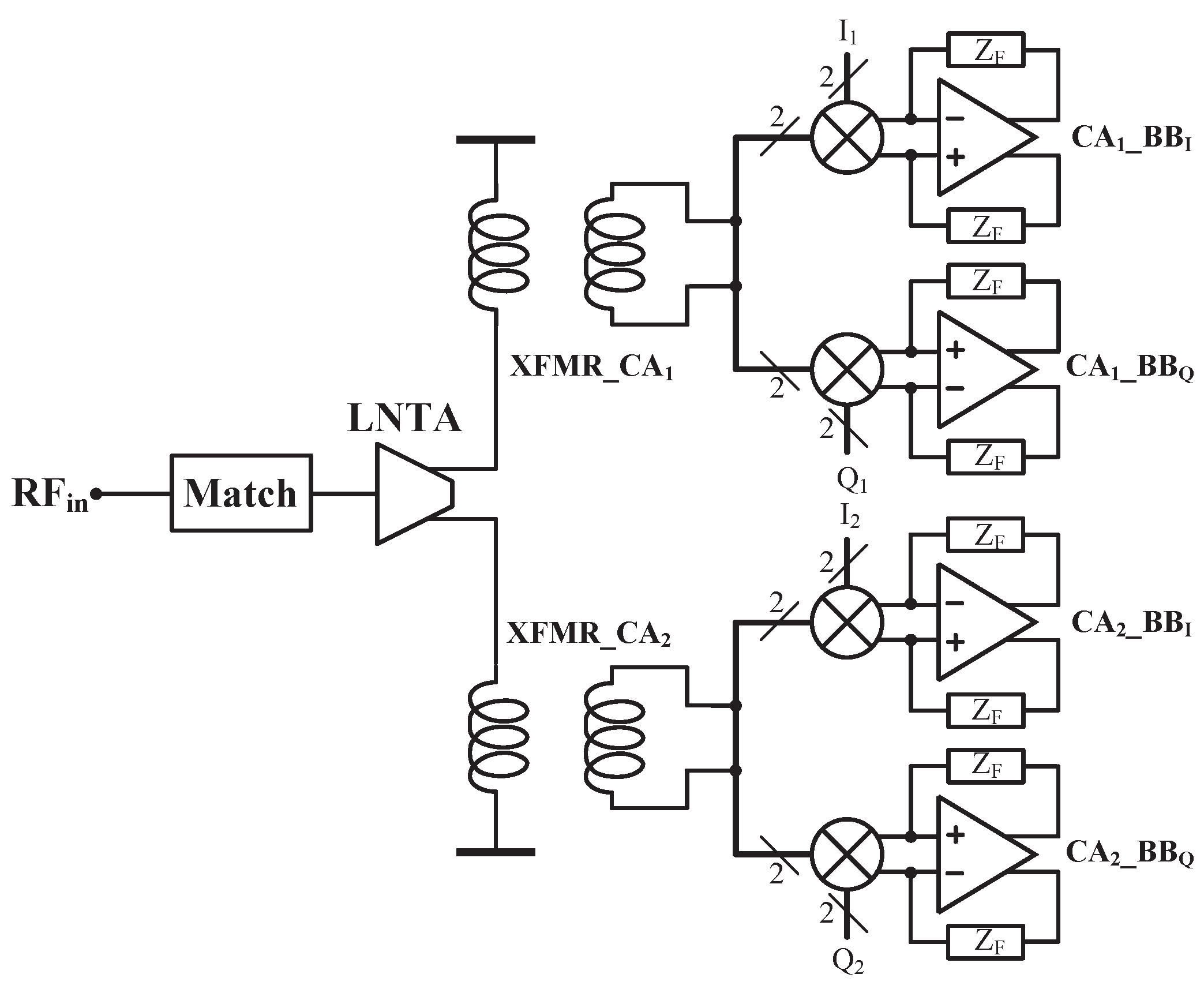
3.1. Three-Coil BALUN LNTA
The three-coil LNTA in
Figure 6 enables CA operation with magnetically-coupled inductors. LNTA tank impedance is lowered by a factor of two due to two inductive coupled loads. With N CA support, the number of magnetically-coupled coils increases linearly. The gain of LNTA is reduced and NF is increased with this approach. Moreover, isolation between different CA paths is limited by the coupling coefficient (
). Two intra-band CA simulation with this approach gives 51.6 dB gain and 3.2 dB NF. Compared to the single-carrier receiver case, 5 dB gain reduction is observed close to the expected 6 dB loss. NF increase is due to the insufficient gain of the LNTA, and more noise contribution from the subsequent stages accordingly. Even with twice the current consumed in LNTA, moderate improvements are achieved with 53 dB and 2.67 dB of gain and NF, respectively.
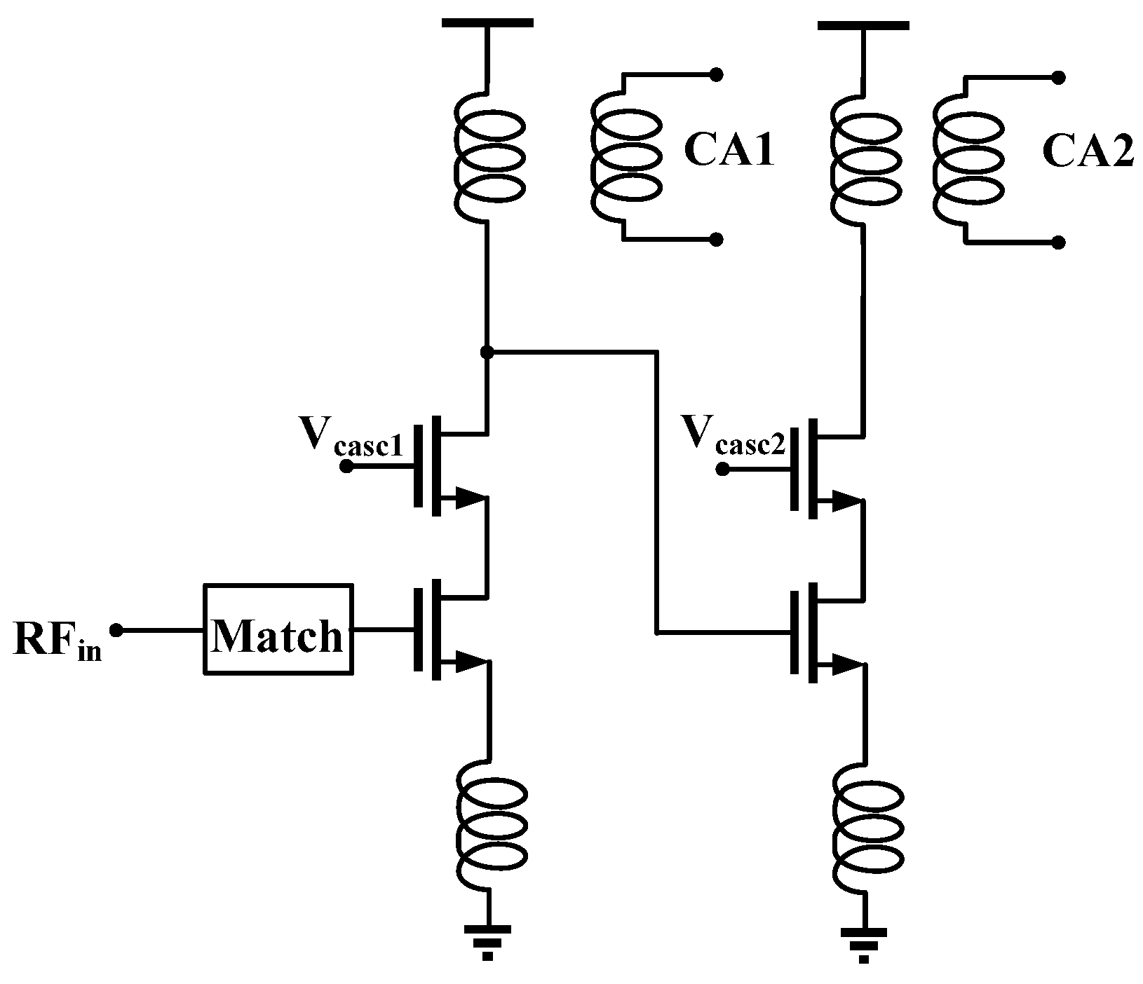
3.2. Two-Stage LNTA
Two-stage LNA is shown in
Figure 7. The second stage is sized smaller so as not to load the first stage of the LNA. CA1 is a single-stage design, and its performance is comparable to the non-CA case. On the other hand, the CA2 path has two-stage active blocks, and even with large degeneration in 2nd stage, linearity is poor due to the cascaded design approach [
10]. NF for CA2 is primarily set by that of first stage design.
Table 1 summarizes the simulation results with the two-stage LNTA approach. All of the performances are comparable to the reference (SISO), with the exception of CA2 path linearity (
).
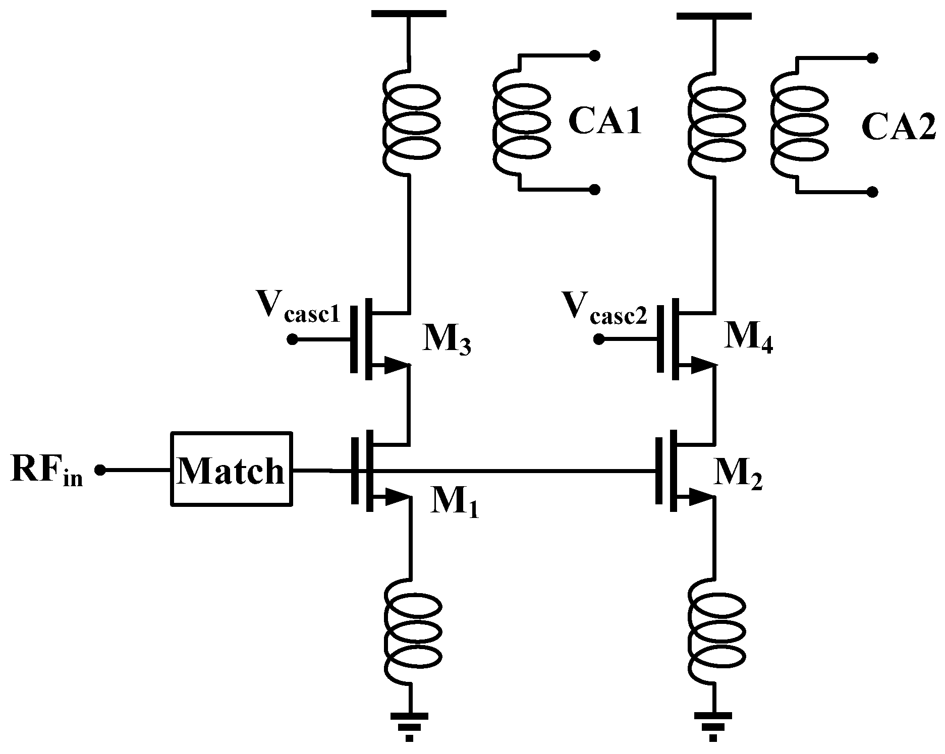
3.3. Split-Cascode LNTA
The split-cascode LNTA shown in
Figure 8 realizes multi-output operation by signal splitting at the cascode node. Trans-conductance (
) is shared between CA paths. Therefore, gain is reduced by
(dB) without current scaling. Even with current scaling by
for N CA, gain reduction of around
(dB) is inevitable due to square-root dependence of gm with respect to the current consumption in CMOS devices (short channel effects are ignored). Shared
dictates small variation in
for different operation modes (non-CA and CA). NF is degraded due to significant noise contribution from the cascode devices and larger contribution from TIA due to smaller LNA gain.
Significant noise contribution due to the cascode devices is coming from the small impedance looking into the another cascode device in intra-band CA operation. In non-CA mode, only the single cascode transistor is enabled and directs the current to either CA1 or CA2. Thus, cascode transistor noise is highly degenerated, giving rise to a small noise contribution. In CA mode, on the other hand, both cascode transistors are enabled, and the small impedance (
) looking into the source node is influencing each other. The noise current out of the cascode devices is expressed as Equations (
5) and (
6) for non-CA and CA mode, respectively.
Table 2 summarizes the simulation results with split-cascode LNTA approach. High NF due to the cascode device is observed, and additional current consumption of the
device gives limited improvement in its NF.
3.4. Cascode Shut-off LNTA
Figure 9 shows the cascode shut-off LNTA.
is separated between different CA paths. Noise contribution due to the cascode device is the same as a conventional LNTA without sharing
as in the split-cascode LNTA. In non-CA operation, gate bias of the second gm transistor is properly ON. At the same time, the cascode bias of CA2 is shut-off to avoid throwing additional current. With this bias scheme, the second
transistor operates in saturation and triode regions in CA and non-CA, respectively. Impedance matching (
) is slightly disturbed due to the change in
and
for different CA modes. Input impedance (
) of the cascode shut-off LNTA is expressed in Equations (
7) and (
8) for non-CA and CA mode, respectively.
where
(=
) is the input impedance of CA1 path (= CA2 path), and it can be expressed as
. Two inductors for source degeneration purposes can be merged into the shared degeneration without losing the property of the cascode shut-off LNTA. Since two inductors are merged in parallel, the size of the inductor decreases, and thus the size of the inductor is minimized accordingly.
Table 3 summarizes the simulation results with cascode shut-off LNTA approach.


