In this Section, we first present a detailed review of major techniques reported in literature to cope with clock jitter effects. Then, we give a quantitative comparison of different techniques in terms of effectiveness to reduce clock jitter effects. In particular, we focus on three most effective techniques and compare them under practical noise. Finally, an overall qualitative comparison of different techniques considering six major metrics are given.
2.1. Review of Previous Work
In literature, a number of techniques have been proposed to reduce clock jitter effects in CTDSM with varying effectiveness [
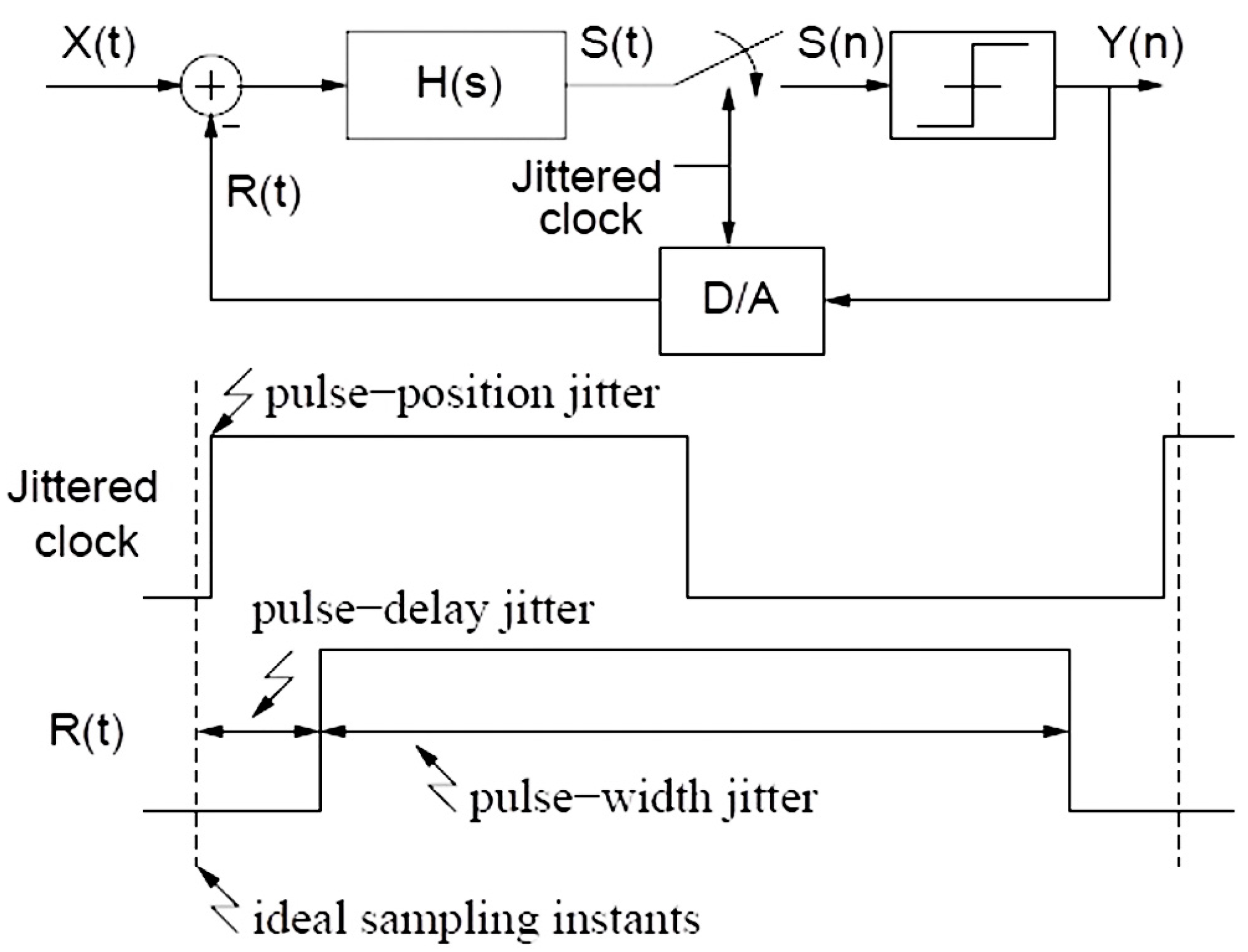
7]. The basic idea behind all methods is to shape the DAC feedback waveform so that an insignificant amount feedback charge is transferred at times of clock transitions, which helps maintain a constant amount of feedback charge in each clock cycle, thus reducing pulse-width jitter.
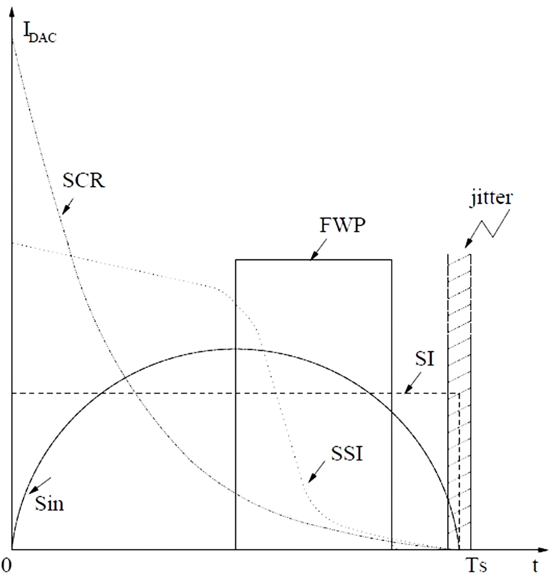
A simple but not very effective technique is to use NRZ (Non-Return-to-Zero) SI (Switched-Current) DAC feedback, whose waveform is shown in
Figure 2 [
7]. In this case, clock jitter only matters when the output changes sign assuming a single-bit quantizer. Or, in other words, clock jitter only affects one rising or falling edge [
6]. Furthermore, it may be helpful to use multi-bit NRZ feedback, because the step height of a multi-bit DAC is smaller and clock jitter induced noise is proportional to that. For example, with a NRZ DAC of 5-bit resolution, 22.5 dB SNR improvement is achieved compared to a RZ DAC feedback, as reported in [
4]. However, the use of NRZ DAC feedback has a price. First, the jitter noise reduction is limited by the number of bits, since a DAC with a large number of bits increases the power consumption of the modulator and introduces linearity problems which has to be corrected by complex DEM (Dynamic Element Matching) or calibration circuits [
3,
4]. Besides, NRZ DAC suffers from memory effects, signal-dependent quantizer jitter and loop delay, though they can be reduced by RZ feedback or additional circuits [
4].
FIR (Finite Impulse Response) DAC feedback is proposed in [
16,
17,
18,
19,
20,
21] to reduce clock jitter effects. The idea is to use a single-bit quantizer with DAC response widened over
n clock cycles so as to average clock jitter effects over
n clock periods. The FIR DAC has comparable jitter noise reduction performance as the multi-bit NRZ DAC, but is linear due to the single-bit quantizer. Using this technique, jitter noise reduction is reported to be up to 18 dB [
16]. However, the jitter noise reduction performance is signal-amplitude dependent and for higher amplitude inputs the results are not as good as those for smaller amplitude inputs [
16,
17]. Besides, it also increases the loop delay of the modulator and may lead to stability problems [
7], which renders synthesis of the modulator with FIR DAC feedback difficult. Finally, extending FIR feedback to multi-bit operation is not readily done [
7].
Another reported technique to reduce clock jitter effects explores the use of sin-shaped DAC feedback [
22,
23] (an example of its waveform is also shown in
Figure 2). In this technique, clock transitions take place when the sin-shaped feedback is at its maximum slope and hence results in a small charge error. To further reduce clock jitter noise, it may be more useful to use multiple sin-shaped pulses per sampling period [
22]. The maximum jitter noise reduction is 17dB, as reported in [
22]. But for sin-shaped DAC feedback, the circuit realization based on phase-locked loop is complex and difficult and it may dramatically increase power consumption. In addition, it is sensitive to loop delay, locking error and phase/amplitude noise of the feedback pulse itself [
22,
23]. Besides, extensibility of the sin-shaped DAC feedback to multi-bit operation is poor [
7]. Synthesis of the modulator with sin-shaped feedback is also more involved than NRZ/RZ feedback.
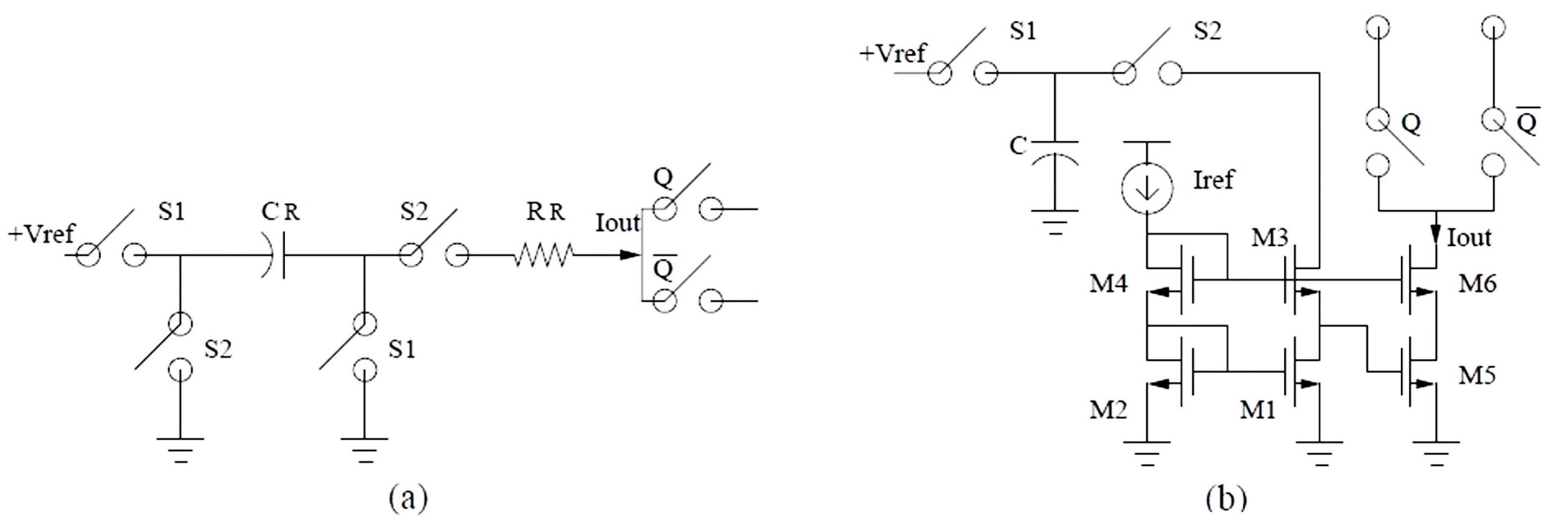
A more effective technique is to employ SCR (Switched-Capacitor-Resistor) feedback [
24], adapted from the switched capacitor feedback in discrete-time modulators. Instead of having the traditional rectangular-shaped SI DAC feedback, which gives a constant current during a clock cycle, an exponentially decreasing feedback current is generated. As illustrated in
Figure 2, the SCR feedback has a waveform that can transfer almost all charges to the integrators before clock transitions and therefore clock jitter causes little charge error. This technique is relatively simple to implement and quite effective to reduce clock jitter effects. An example circuit implementation is shown in
Figure 3a and jitter noise reduction is reported up to 30 dB in some example implementations [
7,
24]. In SCR feedback, the capacitor is first charged during phase
and then switched to the resistor during phase
. A similar technique to generate a quadratically decreasing feedback current is reported in [
25]. But, several drawbacks are associated with SCR feedback. The main drawback is that SCR feedback results in integrator response having high-demand for OpAmp slew-rate and gain-bandwidth product due to the big spike of the feedback current, which greatly increases power consumption of the OpAmp and hence that of the modulator [
7,
24]. Also, recently it has been shown that SCR feedback may severely degrade the alias rejection of the CTDSM [
26,
27,
28]. Besides, synthesis of a modulator employing SCR feedback is more complicated than a modulator using SI feedback [
24]. Finally, SCR feedback may not be well extended to multi-bit operation due to matching and linearization difficulties of reference voltages or capacitors [
7].
To solve some of the problems with SCR feedback while maintaining its effectiveness, Reference [
29] proposes a SSI (Switched-Shaped-Current) DAC feedback technique for clock jitter noise reduction. Instead of generating an exponentially decreasing feedback current over the whole clock period as in SCR feedback, SSI feedback generates a slowly linearly decreasing feedback current in most of the clock period, and then fast decreasing feedback current in the rest of the clock period (as its waveform illustrated in
Figure 2), so that almost all the charge is fed back before clock transitions. An example circuit implementation is shown in
Figure 3b [
29]. The capacitor is first charged during phase
. During phase
, M1, M3, and M5 are in the saturation region and the capacitor linearly discharges until M3 starts to go into the triode region. Then, the capacitor continues to discharge but more slowly until M3 enters deep triode region (drain-source voltage almost 0). By this moment, the current has been slowly decreasing. Subsequently, the capacitor continues to discharge and M5 goes to weak inversion, causing current to drop off dramatically. Meanwhile, M1 should stay in the saturation region. At last, M1 goes to the triode region while M5 turns off, and the current approaches to zero exponentially in a short time duration, in which clock transitions are expected to occur [
29]. The performance of the SSI feedback is comparable to SCR feedback in term of jitter noise reduction. But compared to SCR feedback, it relaxes the demand for OpAmp slew-rate and gain bandwidth and, therefore, should not cause excessive power consumption of the OpAmp. However, the circuit implementation for SSI may be difficult to achieve and needs extensive sizing and tuning. Besides, the technique requires precise control of transistor operation in the saturation region, triode region, and cutoff region, which may not scale well with transitions of transistor technologies in the nano-meter regime. Process variation effects may be detrimental, especially if the circuit is aggressively designed to give a short time duration for clock transitions. Further, like the SCR feedback, synthesizing modulators with SSI feedback is also complicated due to the irregular feedback waveform shape. Finally, regarding extension of the SSI feedback to multi-bit operation, there are two ways to either design multiple current sources or multiple capacitors. However, in either case, the settings of current sources or capacitors are difficult due to the irregular feedback waveform and difficult-to-control transistor operations in different regions. Therefore, extending SSI feedback to multi-bit operation is difficult.
While the above discussed SCR and SSI techniques are quite effective to reduce clock jitter effects by minimizing the jitter-induced charge during clock transitions, they still do not have the convenience of the traditional SI feedback with a rectangular-shaped waveform from design and implementation point of view. However, the traditional SI feedback (with either RZ or NRZ waveforms) is not very effective to reduce clock jitter effects. To address this issue while hoping to retain its advantages, one idea is to maintain the width of the active feedback pulse as fixed as possible [
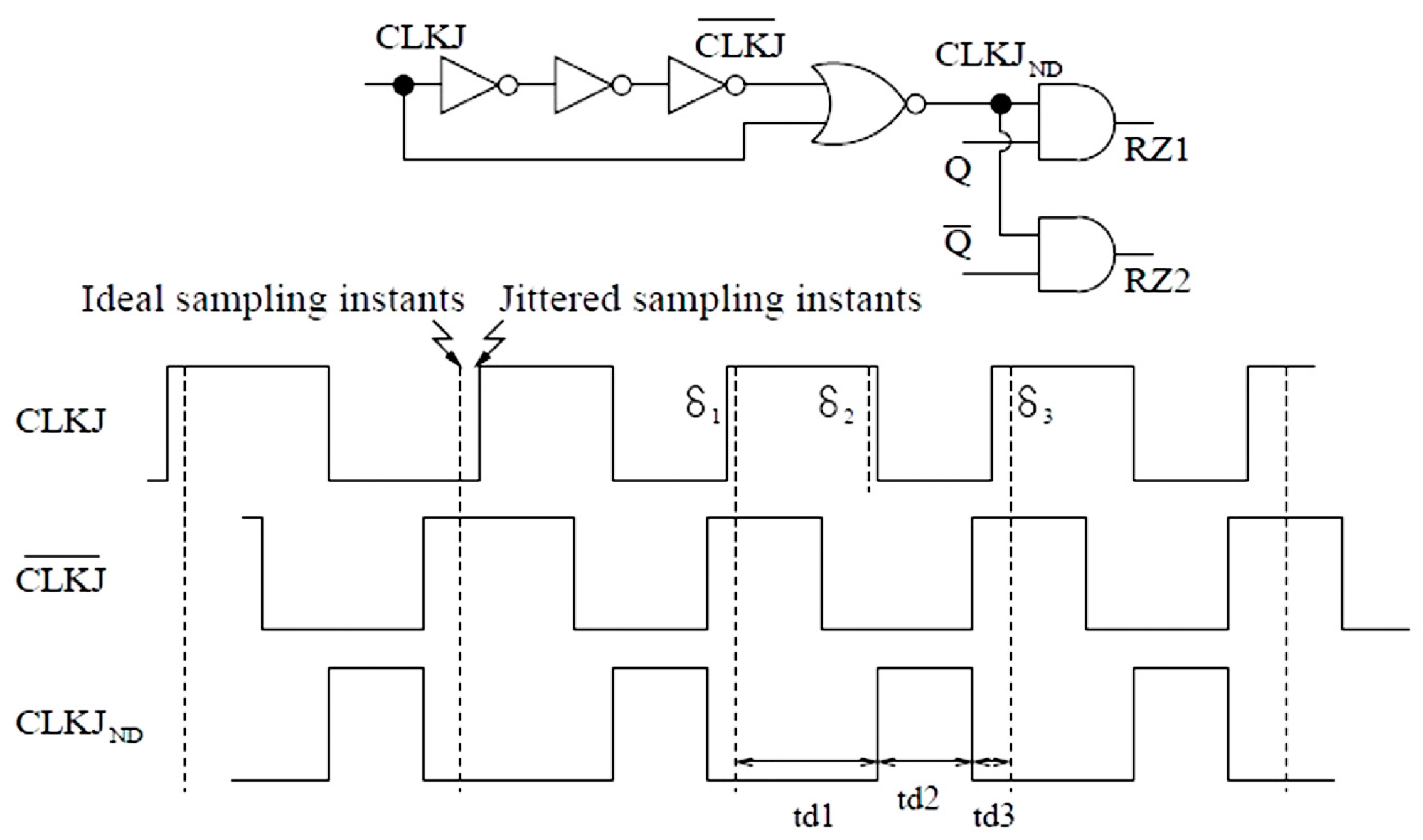
15], hence to reduce the dominant pulse-width jitter. While this is well understood theoretically in literature, it is recent that circuits are proposed to generate a FWP (Fixed-Width Pulse) for active feedback [
30,
31]. One recently proposed method to use FWP RZ feedback is illustrated by the gate-level schematic in
Figure 4 (simplified from the original circuit in [
30,
31]). Assuming
is the original jittered clock with ICJ at rising/falling edges, the resulting signal
has a pulse of fixed-width
set by the first inverter chain. Finally,
is AND with both Q and Q’ (outputs from a single-bit quantizer of a CTDSM) to generate two RZ logic signals, which retain the fixed-width pulse of
. Note that the fixed pulse width
would provide a constant amount of feedback charge, hence eliminating pulse-width jitter otherwise caused by
. The superior effectiveness of the FWP method has been shown in [
15,
30,
31] with up to 33 dB of jitter noise reduction in example designs. However, there are some limitations of the FWP feedback. First, the FWP feedback may not work well in case of very large clock jitter, for instance
=
(i.e., standard deviation of clock jitter is 10% of the nominal clock period), because the fixed-width pulse may not be obtained from the digital gates. Fortunately, practical clock jitter is usually not that large. The other limitation of the FWP feedback is that the circuit in
Figure 4 may only give a pulse width
up to 40% of the nominal clock period. To improve the utilization of the clock period, an alternative circuit is to generate a longer pulse width (e.g., 70% of the clock period) by using additional digital D-flip-flops [
32]. Besides, FWP feedback is more suitable to relatively high-frequency CTDSM, as the delay is achieved by inverter chains and very long inverter chains for a relatively large clock cycle may not be desired in practical circuit implementations due to area and power consumption considerations.
2.2. Comparison of the Techniques in Terms of Effectiveness
In
Section 2.1, we reviewed in detail previous work to reduce clock jitter effects in literature. In the following, we make a quantitative comparison of the techniques in terms of effectiveness of jitter noise reduction. In next
Section 2.3, we make an overall qualitative comparison considering six performance metrics and summarizing their pros and cons.
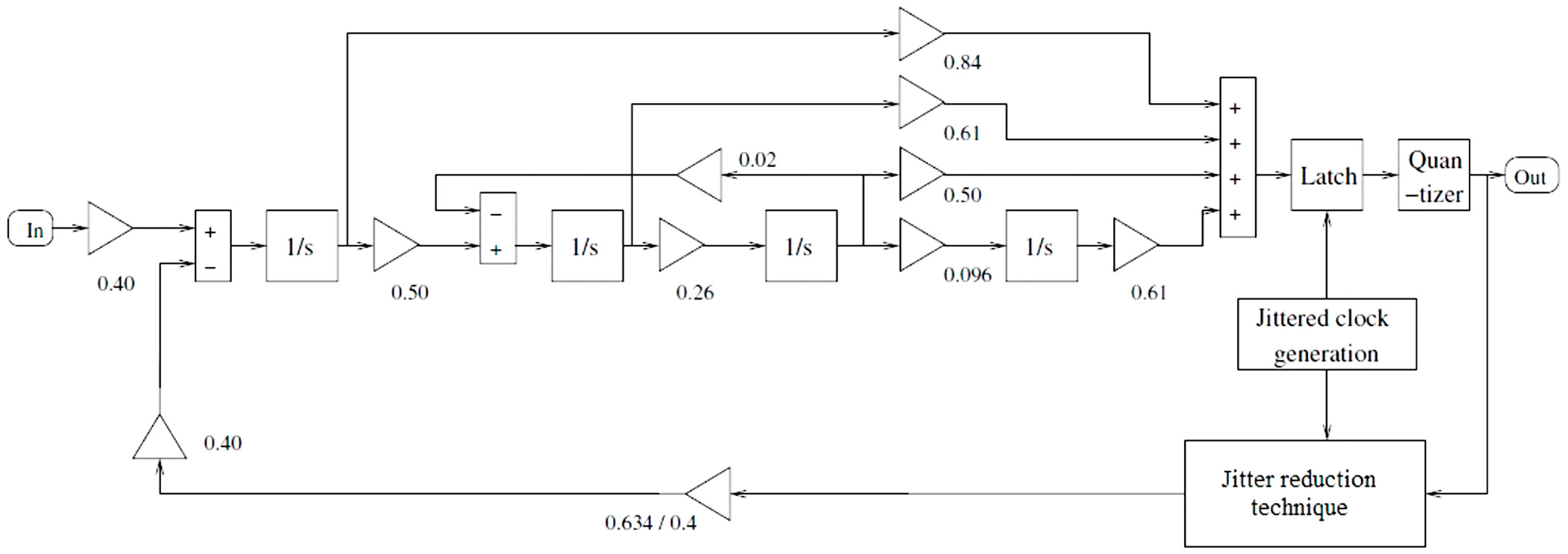
In order to have a quantitative comparison, we performed behavioral simulation on a 4th-order Delta-Sigma modulator shown in
Figure 5 in MATLAB/SIMULINK [
33], and the oversampling ratio was assumed to be 32 to achieve at least 80 dB of SNR with single-bit quantization [
30]. Ideally, the modulator without clock jitter effects would achieve a SNR of 82 dB with SI NRZ feedback. When clock jitter of
(here
is made relatively large to have jitter noise dominate so that one could focus on its effect) was considered, the resulting SNRs for each technique is shown in the second row of
Table 1. It can be recognized that SCR, SSI, and FWP techniques stand out in terms of the effectiveness to reduce clock jitter noise, as they almost achieved the same SNR as the ideal modulator without clock jitter effects. These results were as expected from the discussions in
Section 2.1 and from inspecting their respective feedback waveforms in
Figure 2.
It can be seen that SCR, SSI, and FWP feedback are most effective to reduce clock jitter effects and they are to be used when clock jitter is relatively large. However, it is important to note that they have practical limitations due to noise, namely intrinsic device noise and extrinsic power supply noise. Note that noise is the fundamental reason behind even clock jitter itself (in an oscillator or a phase-locked-loop [
34]) and it similarly causes variation/jitter of the feedback charge in each feedback technique (note that in typical scenarios it is assumed that the noise sources are uncorrelated so the clock jitter itself is independent from the variation/jitter of the feedback charge). In fact, any technique would only be effective to reduce clock jitter effects when the variation/jitter of the feedback charge due to noise is less or equal to that of the clock. Therefore, it is imperative to study their performance under practical noise in contrast to the previous case of without noise. Recently in [
35], the author did a theoretical noise analysis of the SCR, SSI, and FWP techniques to study their limits under external power supply noise (as it is typically dominant over intrinsic device noise) and made an analytical comparison. For the sake of practical comparison in this paper, we designed transistor-level circuits in
Figure 3,
Figure 4 and
Figure 5 and performed electrical simulation in Cadence Virtuoso [
36] on the same modulator as above to derive the SNR assuming typical wide-band white noise (with normalized noise power of
and noise bandwidth of
= 100 MHz as in [
35]). The results are shown in the last three rows of
Table 1 when practical noise was considered. We summarized the major finding below. Under practical noise, each technique indeed has a limitation to reduce jitter effects as the SNRs are clearly below those without noise. The specific limit of each technique mainly depends on the characteristic of the external noise (i.e., noise bandwidth and power) and the specific modulator design (i.e., sampling frequency). Given the same external noise, it is found that the FWP feedback technique is most effective to reduce most clock jitter effects with relatively high sampling frequency (for example, hundreds of MHz), whereas SCR and SSI techniques have best performance with low to medium frequency (for example, tens of MHz or below). When sampling frequency gets lower, the SCR and SSI techniques would be closer to break the limitation from the noise, due to increased filtering of the external power noise from the resistor-capacitor. This trend can be seen in the last three rows of
Table 1 as the SNRs for SCR and SSI techniques saturate to those in the second row of
Table 1 as frequency decreases. Also, note that when frequency is low, FWP feedback is not to be used due to significant power/area overhead, as mentioned before. Finally, note that the above practical simulation results agree well with the theoretical analysis results in [
35].
2.3. Overall Comparison of the Techniques
In
Table 1, we compared different feedback techniques in terms of effectiveness of jitter noise reduction on a common basis with/without noise. However, effectiveness of jitter noise reduction should not be the only factor when objectively evaluating the different techniques and other factors must be factored in to get a better picture. Therefore, for the sake of completeness, we also make a qualitative comparison of the different feedback techniques considering six major factors in
Table 2. First, we rated the techniques in terms of effectiveness (in the second row of
Table 2) by inferring from the results presented in
Table 1.
Next, in terms of synthesis of the modulator: single-bit/multi-bit NRZ/RZ feedback has the rectangular-shaped current, so synthesis of the modulator at system-level design is very easy using Z-transform or modified Z-transform [
37,
38]. The FWP feedback retains the traditional rectangular-shaped current like the RZ feedback, so synthesis of the modulator is easy too. Synthesis of the modulator with FIR, SIN, and SCR feedback is sophisticated due to their special waveforms shapes [
38]. Systematic synthesis of a modulator with SSI feedback is particularly difficult due to its wild and not-well-controlled waveform shapes and significant tuning may be needed. The comparison results are shown in the third row of
Table 2.
Regarding circuit implementation, when compared on a common single-bit modulator design, NRZ/RZ, FWP, and SCR feedback are easier compared to most other methods, particularly the SIN and SSI feedback (see
Section 2.1 for details). Note multi-bit SI DAC was not rated high due to design overhead from possible linearization/matching needs. In addition, the FWP feedback has only moderate demand for performance of active elements, such as OpAmp slew rate and gain-bandwidth product. This demand is slightly more compared to the NRZ/RZ feedback and SSI feedback, but much more relaxed to SCR feedback. Therefore, from this point of view, power consumption of a modulator employing the FWP feedback may be slightly larger than that employing the regular NRZ/RZ feedback and SSI feedback, but much less to SCR feedback. The comparison results are shown in the fourth and fifth row in
Table 2.
Furthermore, it is straight-forward to extend the single-bit NRZ/RZ and FWP feedback from single-bit to multi-bit operations due to compatibility to traditional SI feedback, whereas it is much harder for all other types of feedback due to either matching or linearization issues or additional circuit design overhead. Finally, the RZ or FWP feedback is potentially more robust to process variations, which ease the nominal design. It is noted that process variation does not cause jitter induced charge error but only frequency response shift, which causes little performance degradation. As studied in [
39], even with a large variation range (e.g., −20% to +30%) of the active feedback pulse of
, there is no notable performance degradation (especially if compensation was used). However, under process variation, the current decreasing rate for SCR feedback or the operation region for SSI feedback changes, which may cause increasing jitter induced charge error and frequency response shift. The former may affect the effectiveness of the SCR or SSI feedback on jitter noise reduction. Therefore, a worst-case design for SCR or SSI feedback is preferred under process variation, which may result in over-design or more power consumption. The comparison results in terms of extensibility to multi-bit operation and robustness to process variation are given in the last two rows of
Table 2.
In
Table 2, it can be seen that no single technique is the winner in all aspects. To designers, a general strategy to select a technique may be as follows. If clock jitter is relatively large, performance degradation is accordingly large, therefore SCR, SSI, or FWP may be used. Which of them to select then depend on the sampling frequency. If clock jitter is relatively small (and performance degradation is relatively minor), FIR feedback (or even SI NRZ) may be used as in [
38] and is preferred to SIN feedback. Finally, it should be noted that
Table 2 is mainly meant to provide a qualitative and intuitive comparison in typical application scenarios and thus may be over-simplified.
2.4. Discussion
It should be noted that by no means is the above review of previous work on clock jitter noise reduction complete. The different methods discussed above focus on shaping the feedback waveforms to reduce pulse-width jitters in circuit-level design. In literature, there are also alternative methods that do not rely on shaping the feedback waveform. For example, one reported technique to reduce clock jitter effects is to revise modulator NTF (Noise Transfer Function) at system-level design based on an approximate relationship between the jitter noise power and the modulator NTF [
40,
41]. It was found that modulator NTFs designed with peaking in their passbands may result in lower jitter noise than maximally flat NTFs. For an optimized NTF, the technique is effective to reduce clock jitter noise by up to 9 dB compared to a non-optimized one while quantization noise suppression capabilities are comparable. Nonetheless, having peaking in passband may not be desirable in modulator design. More importantly, such a technique at system-level design is not as effective as SCR, SSI, or FWP feedback techniques.
It should also be noted that all reported methods discussed above consider ICJ [
6] and have been shown effective in this case. For the sake of completeness, we next briefly discuss the case of Accumulated Clock Jitter (ACJ) [
6]. For ACJ, the sampling instants are considered as the accumulation of all previous sampling intervals and become:
where
is jitter of the clock cycle
(in contrast to jitter of the rising/falling edge in the ICJ) and is modeled as i.i.d Gaussian noise [
6]. Though the statistics of
are independent and stationary, those of
are not. ACJ is typically caused by voltage controlled oscillators with limited stability [
6]. SNR of the modulator with ACJ degrades significantly when
of
increases as in the case of ICJ. When
of
is in the range of
to
(which is the range typically studied for ICJ), the SNR of the modulator is only marginally improved by 3 to 5 dB when either SCR, SSI or FWP feedback is applied to reduce clock jitter noise. It is obvious that any of the feedback techniques is much less effective for ACJ than ICJ. A very similar observation is reported in [
42] when SCR feedback is applied but found not effective for ACJ.
In typical circuit implementations, the clock is usually derived from Phase-Locked-Loop (PLL), which is neither truly ICJ (with white phase noise) nor ACJ (with large noise skirts), but a complex combination of them. In this case, SCR, SSI, or FWP may still be useful for jitter noise reduction based on the analysis results in [
12].


