In this section, the sensitivity factor of the SCA, TCA and DCA are extracted based on the total gain and sensor capacitance. To design a chopper amplifier, it is important that the relation between the bandwidth and the noise corner frequency given in (4) is respected. As a result, a reference amplifier with a particular gain and a valid relationship between the bandwidth and the noise corner frequency is considered to compare the performance of different chopping techniques for different gains.
4.1. Reference Amplifier
It is assumed that the reference amplifier has a gain of G0 and the current and dimensions of the input transistors maintain a valid relationship between the bandwidth and the noise corner frequency.
The characteristics of the chopping amplifiers for different gains are extracted based on characteristics of the reference amplifier. It is assumed that all amplifiers used in the chopping systems in this paper have a bandwidth of at least ten times larger than their noise corner frequency. There are different methods of changing the current and dimensions of the transistors to achieve an amplifier gain such that:
where
G is the amplifier gain which is
K times the gain of the reference amplifier. The possible approaches of changing the gain while maintaining the condition set in (4) are listed as cases in
Table 1 along with the effect they have on different circuit metrics. In all of these cases, the load capacitance
CL is kept constant. It is noted that any second order non-idealities are neglected in
Table 1. Moreover, the minimum allowed value of length and width of the transistors depend on the technology considered for the design.
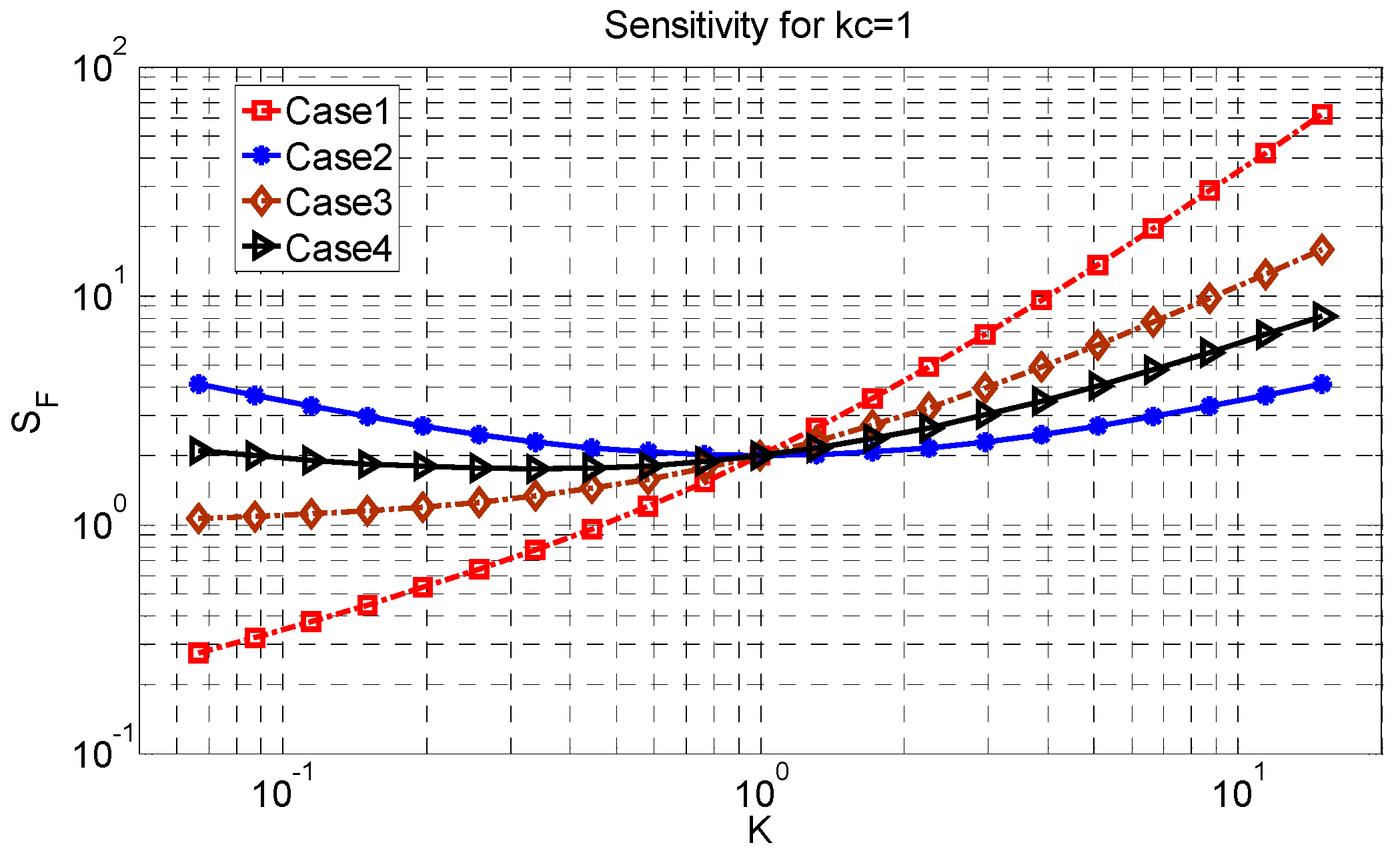
Figure 3 and
Figure 4 show the effect of changing the gain on the sensitivity factor for two values of the loading factor in the reference amplifier (
Kc = 0.01 and 1). The sensitivity factor and gain of these figures are normalized based on the sensitivity factor and gain of the reference amplifier. In each figure, the sensitivities for the four possible cases in
Table 1 are considered to achieve the desired gain.
As shown in
Figure 3, with increasing gain, the thermal noise and input capacitance vary as shown in
Table 1.
Cgg is changed by a factor of
K in all of the cases which implies that the loading factor is increased by a factor of
K. As a result of the gain variation, the loading factor is changed from 0.001 to 0.1, having a negligible impact on the sensitivity factor in this case as it remains much smaller than 1. Variation of the thermal noise depends on the considered case. As shown in
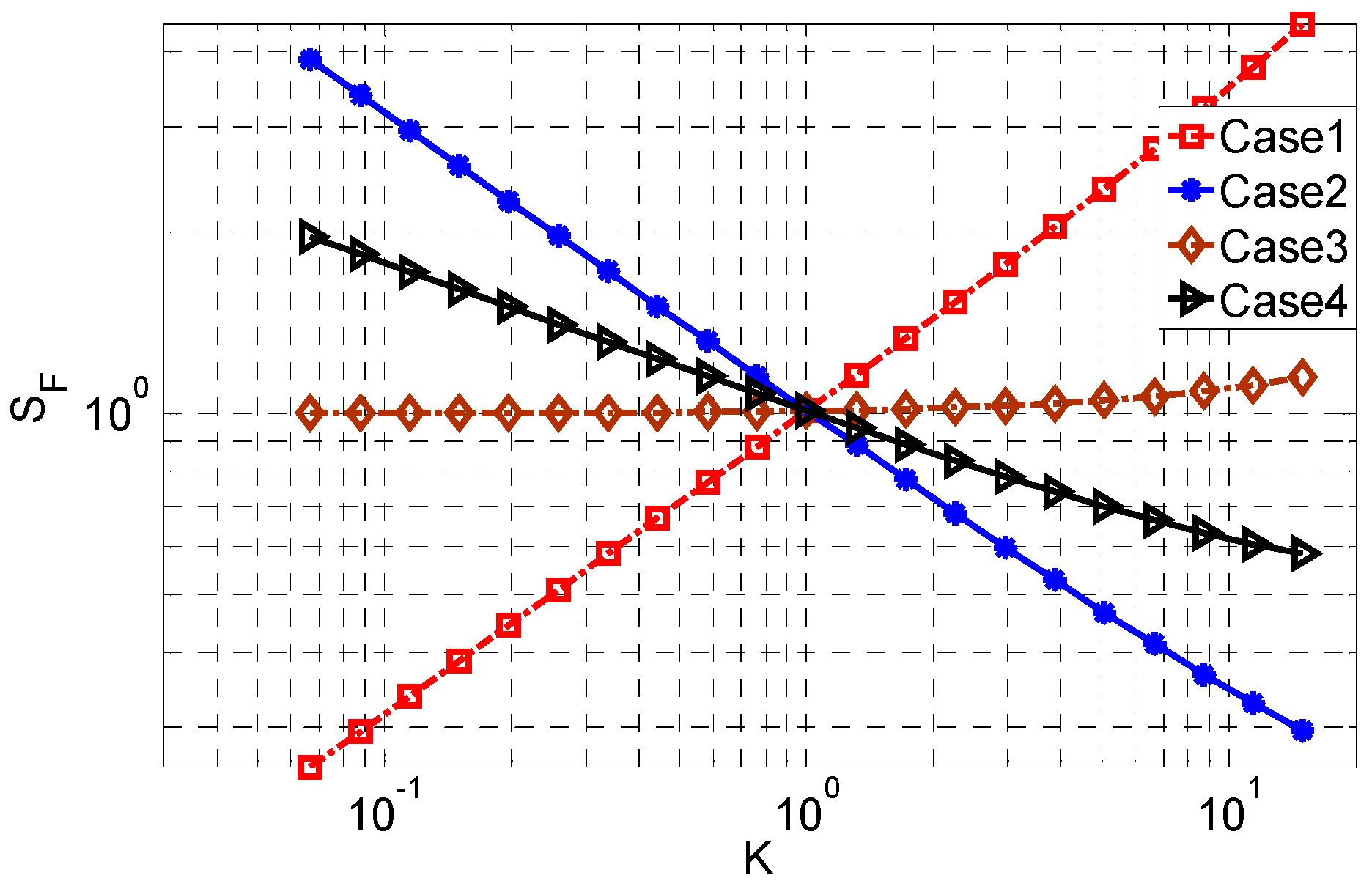
Figure 3, with increasing
K, the sensitivity factor is increased in case 1, decreased in cases 2 and 4 and almost constant in case 3. The trend in the sensitivity factor is thus the same as the trend of the thermal noise. This means that the effect of the loading factor on the sensitivity factor is negligible and the sensitivity factor is affected solely by the thermal noise.
The sensitivity factor based on varying
K for a loading factor of 1 in the reference amplifier is shown in
Figure 4. In this case, the loading factor varies from 0.1 to 10. As a result, it affects the sensitivity factor. As shown in
Figure 4, with increasing
K, the sensitivity factor is increased in case 1 but in cases 2, 3 and 4, there is an optimum value. This stems from both the thermal noise and loading factor variation with
K. In case 1, both the thermal noise and loading factor are increased by increasing
K, causing an ascending trend in the sensitivity factor. However, in cases 2, 3 and 4, the loading factor is increased but thermal noise is decreased. Since the effect of loading factor in this case is not negligible, an optimum value of
K to achieve the lowest sensitivity factor can be observed. Accordingly, when the loading factor is 1, the effect of the loading factor on the sensitivity factor cannot be neglected.
To be able to compare the sensitivity factors of the different chopping techniques in the following analysis, the total gain of the circuit is considered to be set to
Gt and the gain of the reference amplifier is considered to be of
G0. Equation (18) shows the relation between
G0 and
Gt implying that the total gain is
G0 times larger than the gain of the reference amplifier.
In the following sections, the sensitivity factor and power consumption of the three chopping techniques considered in relation to the reference amplifier will be analyzed.
4.2. Single Chopper Amplifier
In the SCA, the signal is chopped at the frequency
fchop. After modulation, the signal is amplified by the amplifier. Next, the signal is demodulated to the baseband where it will be filtered by a low pass filter. For an SCA gain of
Gt,
K is made to be equal to
G0. Out of the four cases in
Table 1, cases 1, 2, 4 can be applied in the SCA to vary the gain. Case 3 cannot be applied because achieving a large gain by changing the dimensions and keeping the power constant is not possible.
The sensitivity factor of the SCA is given by:
where
Vn,SCA is the thermal noise of the amplifier and
KC,SCA is the loading factor of the amplifier. The sensitivity factor for cases 1, 2 and case 4 based on the reference amplifier are given below in (20)–(22), respectively.
where
Vn,0 is the reference amplifier noise floor voltage and
KC0 is the reference loading factor.
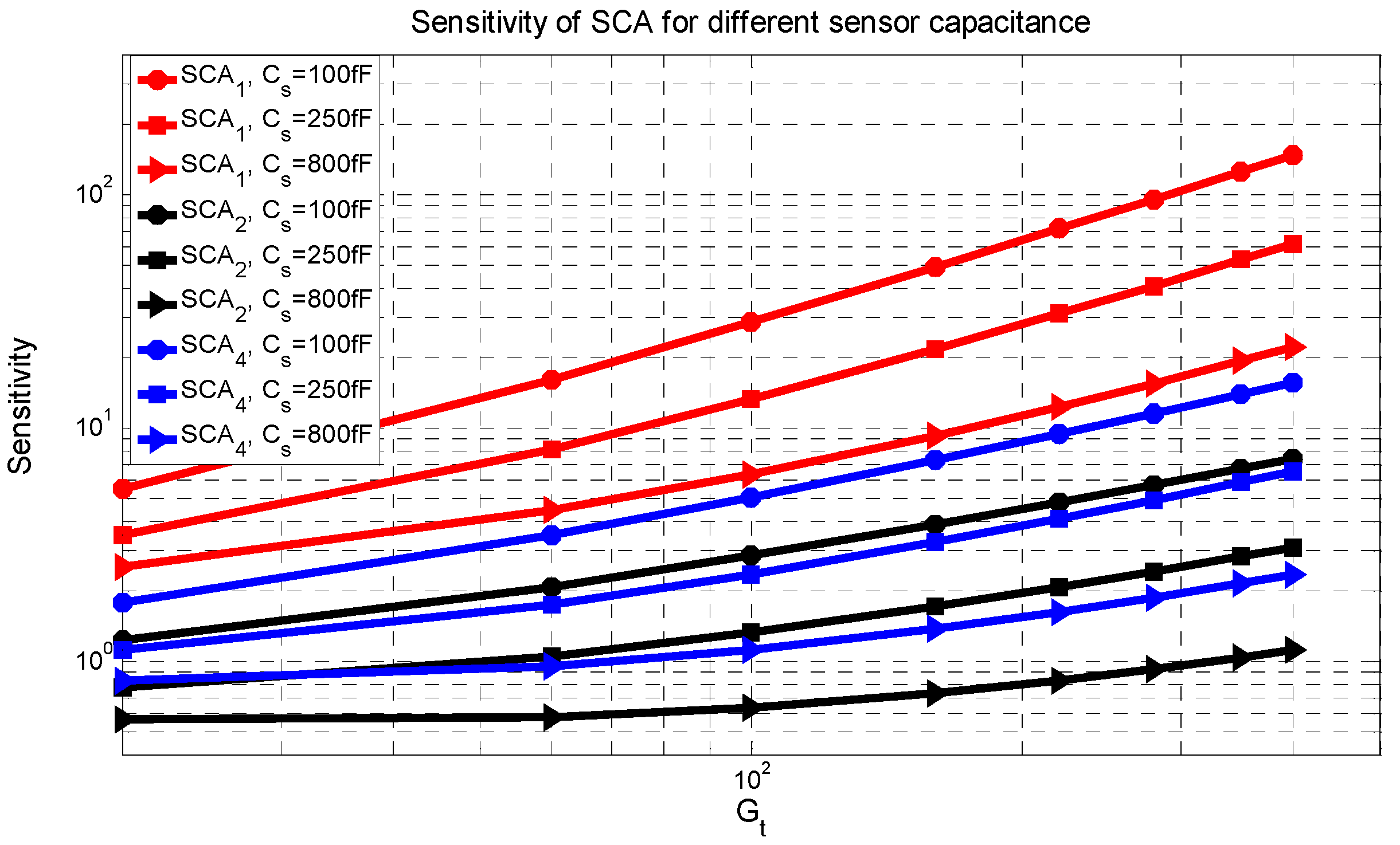
The sensitivity factor of the SCA versus the total gain is shown in
Figure 5 for three sensor capacitances of 100 fF, 250 fF and 800 fF and for cases 1, 2 and 4. As shown, increasing the gain increases the sensitivity factor and the increase is larger for a smaller sensor capacitance because it has a larger loading factor. Comparing these three cases,
SF,SCA2 represents the lowest sensitivity factor, since the thermal noise is smaller in case 2.
The power consumption is independent of the sensor capacitance and in cases 1, 2 and 4, it is equal to:
From these equations, it can be concluded that although SCA,2 has better sensitivity, it consumes more power.
The power-sensitivity factor for the SCA in cases 1, 2 and 4 is given by:
From these equations, it can be concluded that increasing the gain will increase the power-sensitivity factor in cases 2 and 4 but in case 1 it depends on both the value of the gain and the loading factor. The power-sensitivity in case 2 is larger than in case 4. Moreover, a smaller sensor capacitance results in a larger power-sensitivity factor outlining the limitations of the SCA topology to accommodate small sensor capacitances.
4.3. Two-Stage Single Chopper Amplifier
In the TCA, the signal is also chopped by the frequency
fchop. After modulation, the signal is amplified by the first and second amplifiers. Next, the signal is demodulated to the baseband where it will be filtered by a low pass filter. Since both amplifiers in the TCA are operating at the same frequency, it is important to select a chopping frequency that is at least 10 times larger than both noise corner frequencies of the amplifiers. To analyze the performance of the TCA with the same total gain as the SCA, it is assumed that the first amplifier and the second amplifier have gains of
G1 and
G2 that are varied from 1 to
Gt (i.e.,
) as outlined by:
G1 and
G2 are the gain of the first and second amplifiers, respectively and
K (distribution of gain between two stages) should be in the range shown in (31) to have the total gain of each amplifier range from 1 to
.
The second amplifier in the TCA has a constant load capacitance of
CL but the load capacitance of the first amplifier is the input capacitance of the second amplifier. As a result, changing the dimensions of the second amplifier to change the gain will affect the characteristics of the first amplifier. A larger gain in the second amplifier will result in a larger input capacitance and a larger load capacitance for the first amplifier. This will decrease the bandwidth of the first amplifier. As a result, the effect of changing the load capacitance of the first amplifier should be considered when distributing the gain between the two stages. The TCA is designed in such a way that the bandwidths of both amplifiers are at least 10 times larger than the noise corner frequency. The characteristics of the possible methods to change the gain of the first amplifier by a factor of
K when compared to the reference amplifier and the gain of the second amplifier by a factor of 1/
K are listed by case in
Table 2 and
Table 3; respectively.
As shown in
Table 2 and
Table 3, different combinations of cases for the first and second amplifiers are possible to attain the required gain from each amplifier. However, only case combinations where the chopping frequency fulfills (4) for both amplifiers can be considered. With these conditions, only the combinations of cases in
Table 4 are suitable. The first case index in this table represents the applied case in the first amplifier and the second index shows the applied case in the second amplifier. Because of the limitation in the noise corner frequencies and the chopping frequency, all of these cases are valid for
K larger than 1. This means that in the TCA, the gain of the first amplifier should be larger than the gain of the second stage. As a result, it is impossible to implement a small gain in the first stage to realize a small loading factor. Between these cases, the maximum sensitivity is achieved by applying case combination 21. However, the power consumption for this case combination is the largest.
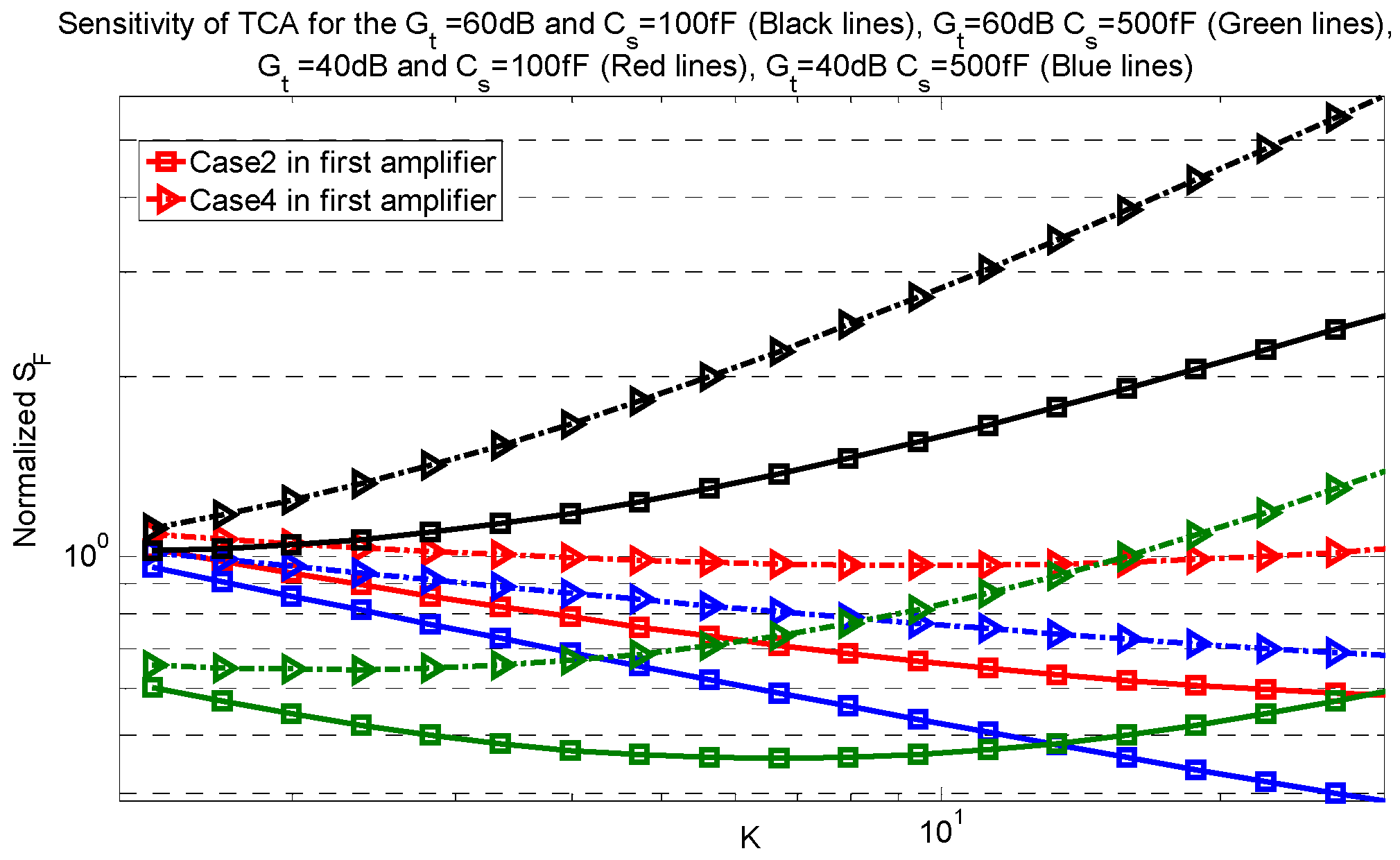
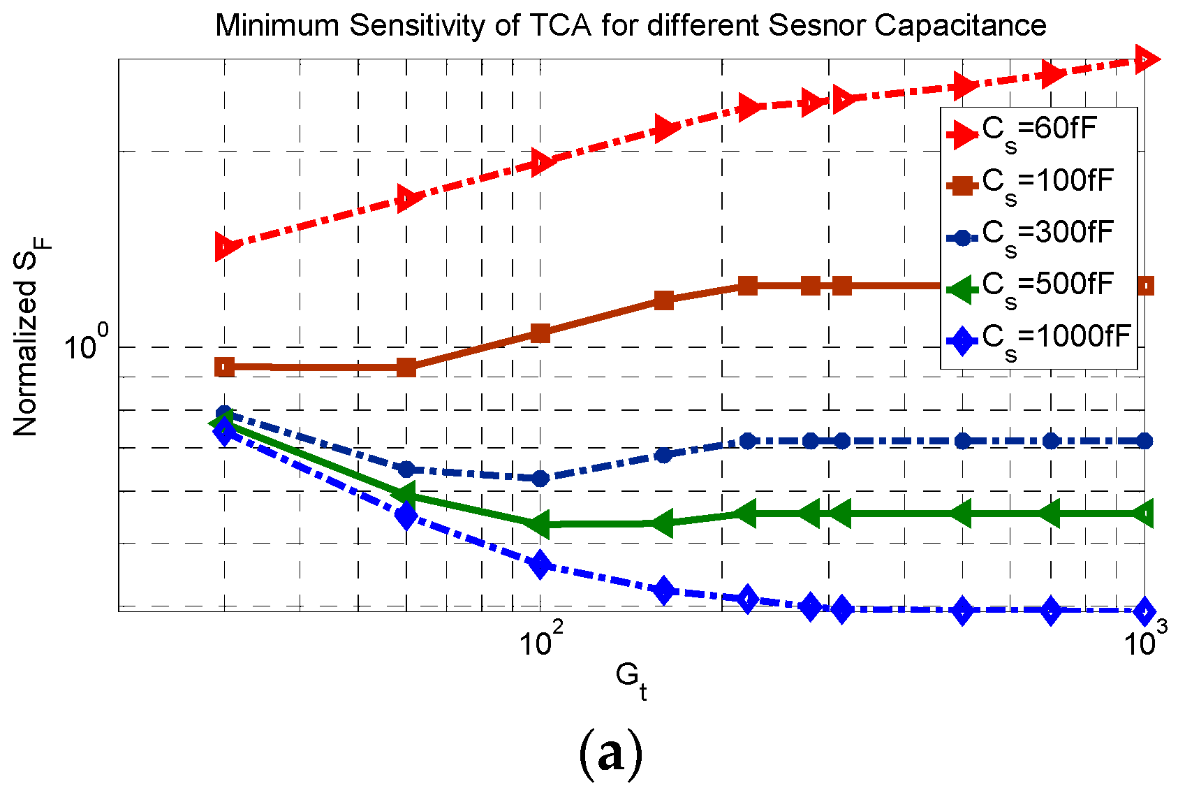
The sensitivity factor of the TCA for total gains of 60 dB and 40 dB and two different sensor capacitances of 100 fF and 500 fF versus
K are shown in
Figure 6. Since the second amplifier does not have a sizable effect on the sensitivity factor of the TCA, only the sensitivity factors based on the possible cases for the first amplifier are shown. As shown at this figure, at the same gain and sensor capacitance, case 2 has a smaller sensitivity factor than case 4. With increasing
K, the trend in sensitivity factor is dependent on both the gain and the sensor capacitance. At a gain of 40 dB and a sensor capacitance of 500 fF, the sensitivity factor decreases for an increasing
K. This is because the effect of the loading factor is negligible and when the gain of first amplifier is increased; the thermal noise is decreased resulting in a decreasing trend in the sensitivity factor. However, for larger total gain or smaller sensor capacitance, the loading factor is not negligible when the gain of the first amplifier is increased. This results in an optimum value based on the value of
K. At a gain of 60 dB and a sensor capacitance of 100 fF, where the effect of the loading factor is dominant over the thermal noise on the sensitivity factor. As a result, increasing the gain of the first amplifier causes the sensitivity factor to have an increasing trend.
Note that minimum power consumption is achieved when K equals 1, which occurs when both amplifiers have the same gain. Comparing the power consumption in different cases shows that case 4 in the first amplifier results in a lower power consumption, although its sensitivity factor is larger.
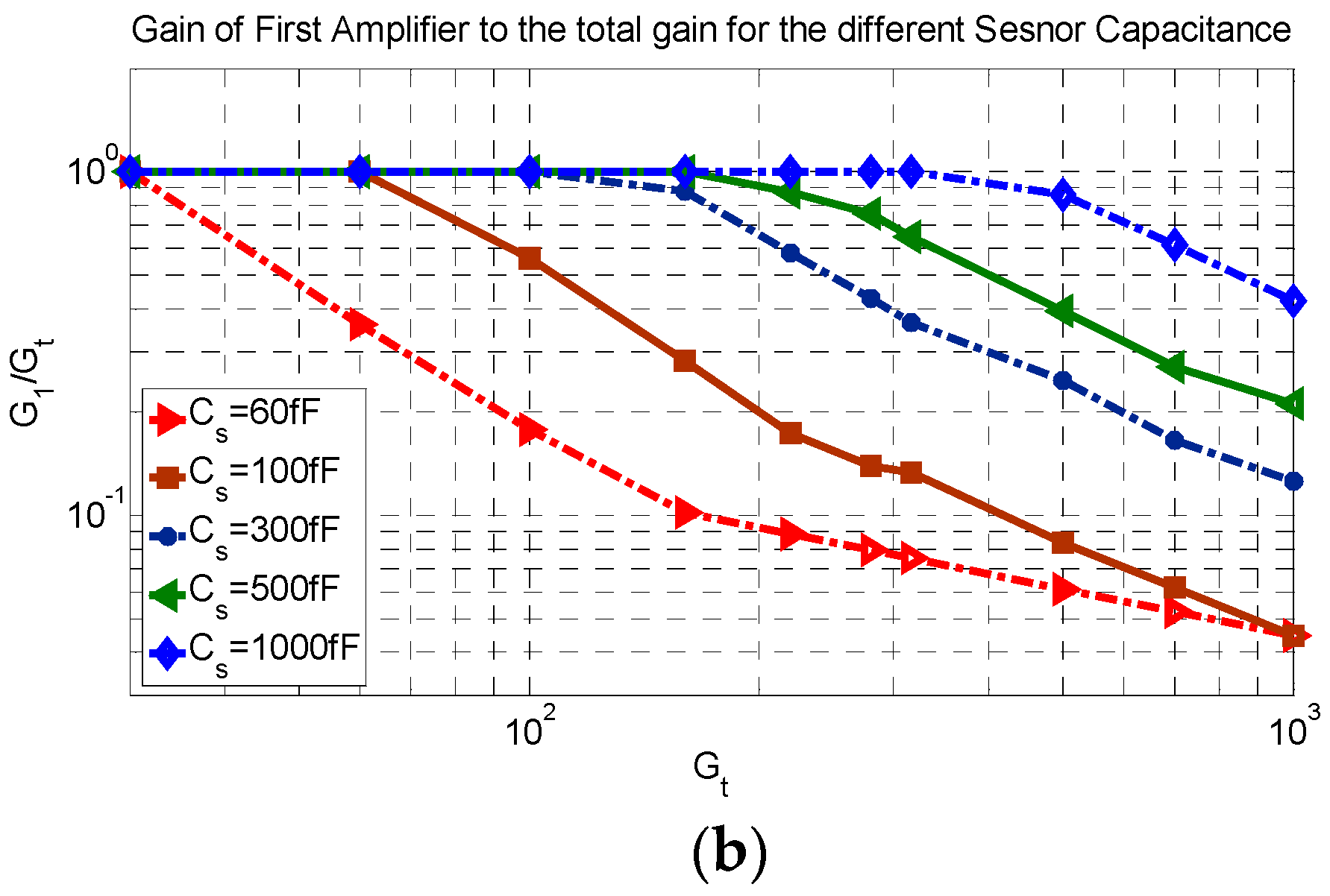
The minimum sensitivity factor of the TCA for different total gains and different sensor capacitances is shown in
Figure 7a and the ratio of gain of the first amplifier to the total gain related to the minimum sensitivity of TCA is shown in
Figure 7b. For each gain and sensor capacitance, the sensitivity factor is based on the possible gain adjustment cases, the range of
K is considered and the minimum sensitivity factor is extracted. As a result, for each gain and sensor capacitance, the value of
K and the applied cases can be different.
As shown in
Figure 7b, at a smaller
Gt, the ratio of the first amplifier gain to the total gain is 1 which means that the minimum sensitivity factor is reached when all the amplification is done at the first stage and the second stage has the gain of 1. Note that this case corresponds to the SCA, since all the gain is achieved using only one stage and the second gain stage is not necessary. As the total gain is increased, the ratio of gains starts to decrease based on the value of the sensor capacitance. For a smaller sensor capacitance, the ratio starts to decrease for a smaller gain but for the larger sensor capacitance, the ratio remains at a value of 1 and then starts to decrease for a larger gain. This difference is justified by the loading factor.
Increasing the gain increases the power consumption and the power consumption for a large sensor capacitance is higher. This is because in this condition, all amplification is done by the first amplifier which results in a larger power consumption. Systems with a smaller sensor capacitance can have lower power consumption because the amplification is distributed between the two stages.
4.4. Dual Chopper Amplifier
In the dual chopper amplifier, two different and independent chopping frequencies are applied. Each chopping frequency is defined by the corner frequency of the related amplifier. This characteristic gives an extra degree of freedom when distributing the gain between the two stages which makes it possible to have a smaller sensitivity factor. As with the TCA, the capacitance of the input pair of the second amplifier is the load capacitance of the first amplifier. As a result, changing the gain distribution between the two stages changes the load of the first amplifier, which affects its bandwidth and power consumption. If the first and second amplifiers have a gain of
G1 and
G2, respectively, as described in (29) and (30), there are different ways to change their gains and all of the combinations in
Table 2 and
Table 3 can be applied to reach the desired gain.
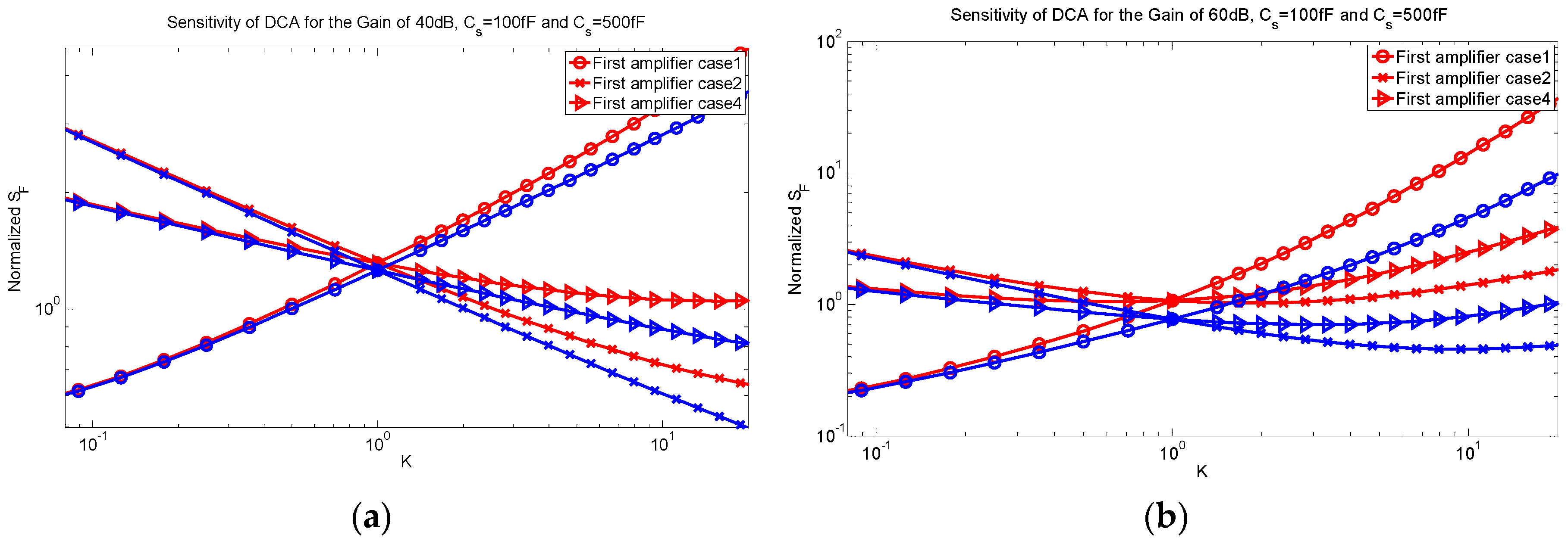
The sensitivity factor of the DCA for sensor capacitances of 100 fF and 500 fF for gains of 40 dB and 60 dB are shown in
Figure 8a,b. In these two figures, the sensitivity factor based on
K and three possible cases for the gain modification of the
first amplifier are shown. Since the effect of the second amplifier on the sensitivity factor is small, it is not considered here. This is the case because the total gain can be distributed to ensure that the gain of the first amplifier is high enough to suppress the thermal noise of the second stage, or that the gain of the second amplifier is high enough to result in a small thermal noise from the second stage.
As shown in
Figure 8a, increasing
K decreases the sensitivity factor for cases 2 and 4 and increases it for case 1. With increasing
K, the thermal noise is decreased in cases 2 and 4 and increased in case 1 but the loading factor is increased in all cases. At this total gain, the effect of the thermal noise is dominant rather than the loading factor. As a result, the sensitivity factor has the same trend as the thermal noise. At a gain of 40 dB and a sensor capacitance of 500 fF, the minimum sensitivity factor is reached when
K is maximized. In other words, all amplification is done in the first stage and the second stage has a gain of 1. This condition simplifies to the SCA. For a gain of 40 dB and a sensor capacitance of 100 fF, the minimum sensitivity factor is reached with the minimum possible
K and applying case 1 for the first amplifier. The sensitivity factor in this case is given by:
A minimum K means the gain of the first amplifier is equal to 1 and all amplification is done in the second stage. For a small sensor capacitance (i.e., 100 fF), the effect of the loading factor is more important and the first amplifier acts as a buffer to keep the parasitic capacitance at the sensor node low, while being able to drive the larger capacitance of the second amplifier that implements the required gain.
The sensitivity factor for a gain of 60 dB is shown in
Figure 8b. For cases 2 and 4, increasing the
K decreases the thermal noise and increases the loading factor, which creates the presence of an optimum value. When
K is smaller than the optimum value, the effect of the thermal noise is dominant and when
K is larger than the optimum value, the effect of the loading factor becomes dominant. A minimum sensitivity factor is reached when the first amplifier has the gain of 1 and case 1 is applied. This mitigates the loading factor and results in the smallest sensitivity factor. It should be emphasized that case 1 is reached by decreasing the transistor lengths and it should be checked whether it is possible or limited by technology geometry.
The power consumption of the DCA for the different cases can be extracted from
Table 2 and
Table 3. The DCA has the maximum power consumption when the first amplifier is in case 1 and
K is the smallest possible value, or when first amplifier is in case 2 and
K is the maximum value. The optimum power consumption is reached for the DCA for the same gain in the first and second stages.
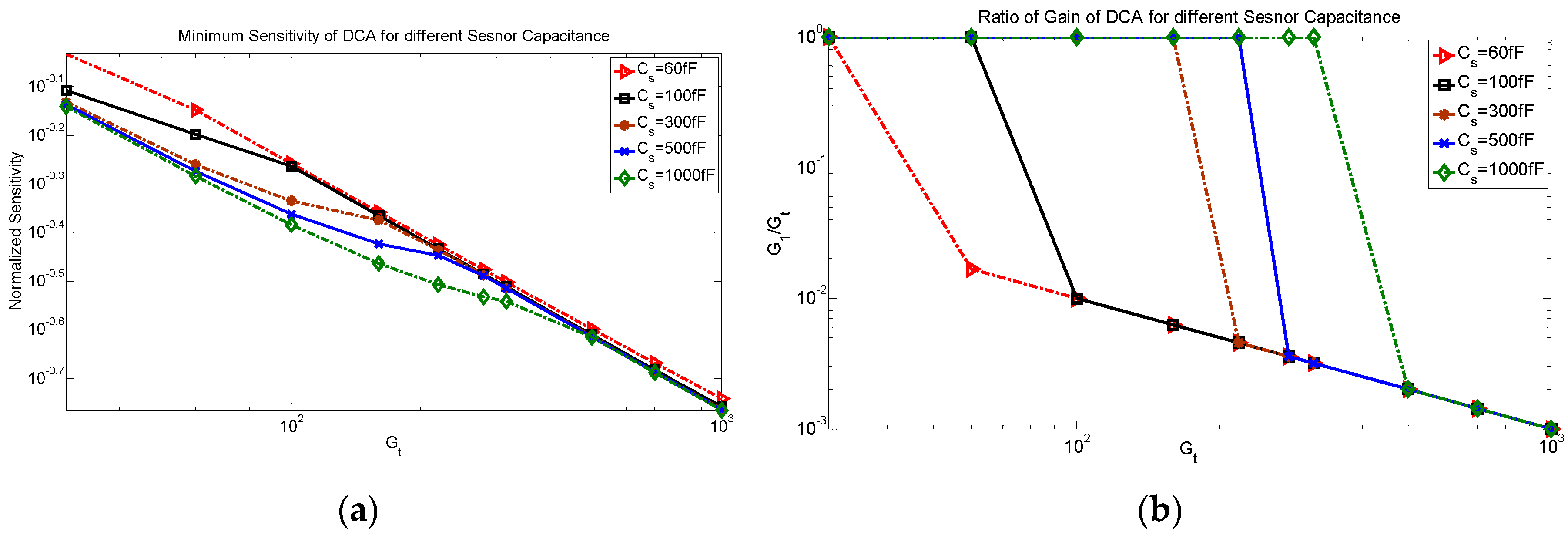
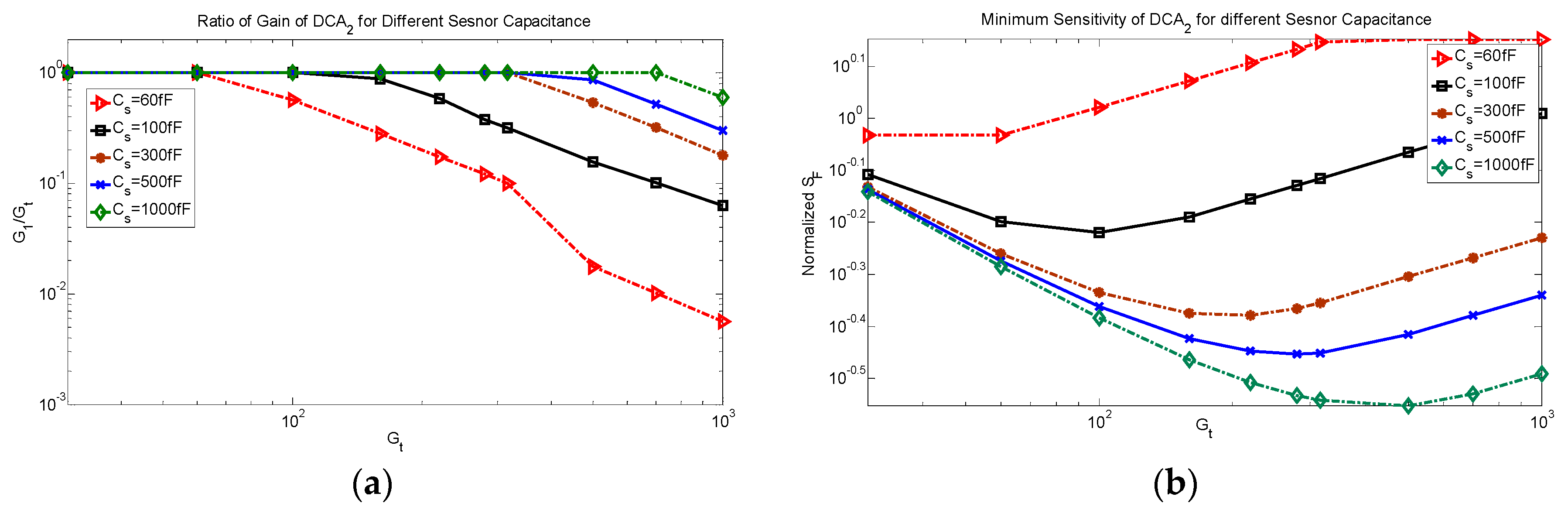
The minimum sensitivity factor of the DCA versus the total gain and for different sensor capacitances is shown in
Figure 9a. These values are obtained by analyzing the sensitivity factors for the different gain modification cases and different values of
K. As shown in
Figure 9a, increasing the total gain decreases the minimum sensitivity factor. This can be explained by
Figure 9b, which shows the ratio of the gain of the first amplifier to the total gain for the related minimum sensitivity factor. As shown, the ratio changes based on the total gain and the sensor capacitance, which is justified by the loading factor. Many distributions result in a negligible loading factor but the minimum sensitivity factor is reached when the first amplifier has a gain of 1 which is attained by case 1 and all amplification is done at the second amplifier via case 2. In this condition, the minimum thermal noise is achieved.
As shown in
Figure 9a, increasing the total gain decreases the sensitivity factor because the thermal noise is decreased and the DCA can maintain the loading factor small.
To reach the smallest sensitivity factor in the DCA when case 1 is applied, the length of the input transistors should be decreased to have a smaller loading factor. However, the technology can limit the level of scaling that can be achieved. As a result, another option is considered. The sensitivity factor of the DCA is extracted while the length of the input transistors is kept constant and this DCA is named DCA
2.
Figure 10a shows the minimum sensitivity factor of DCA
2 and
Figure 10b shows the ratio of the gain of the first amplifier to the total gain to achieve the minimum sensitivity factor. As shown in
Figure 10a, for a small sensor capacitance, the sensitivity factor is increased by increasing the gain. For this condition, the effect of the loading factor is dominant over the thermal noise and because of the assumed technology limitation, the loading factor cannot be reduced. For a larger sensor capacitance, an increasing gain leads to an initial decrease in the sensitivity factor and then an increase is observed. This is because the effect of the thermal noise is dominant for small gain increases but for a large increase, the effect of loading factor becomes important. As shown in
Figure 10b, for a small gain, the gain of the first amplifier is equal to the total gain. As the gain is increased, the ratio drops. The value of the total gain for which the ratio starts dropping depends on the sensor capacitance. However, the gain of the first amplifier cannot be as small as 1 because of the limitation in decreasing the transistor length and this results in a larger sensitivity factor compared to the original DCA for the same condition.
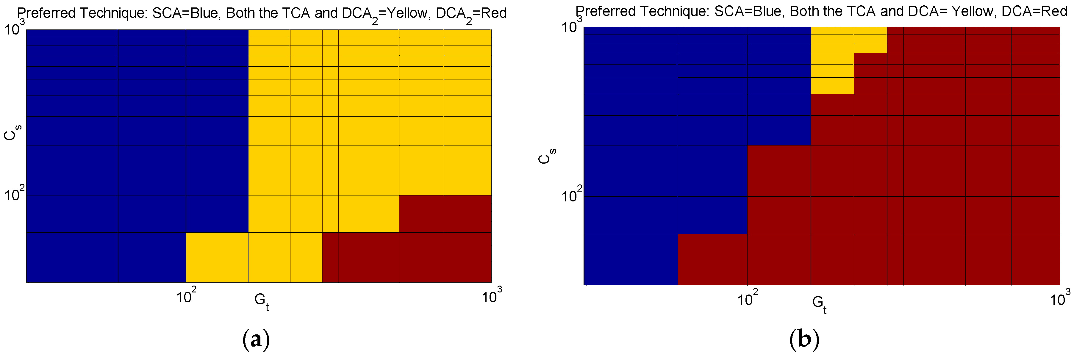
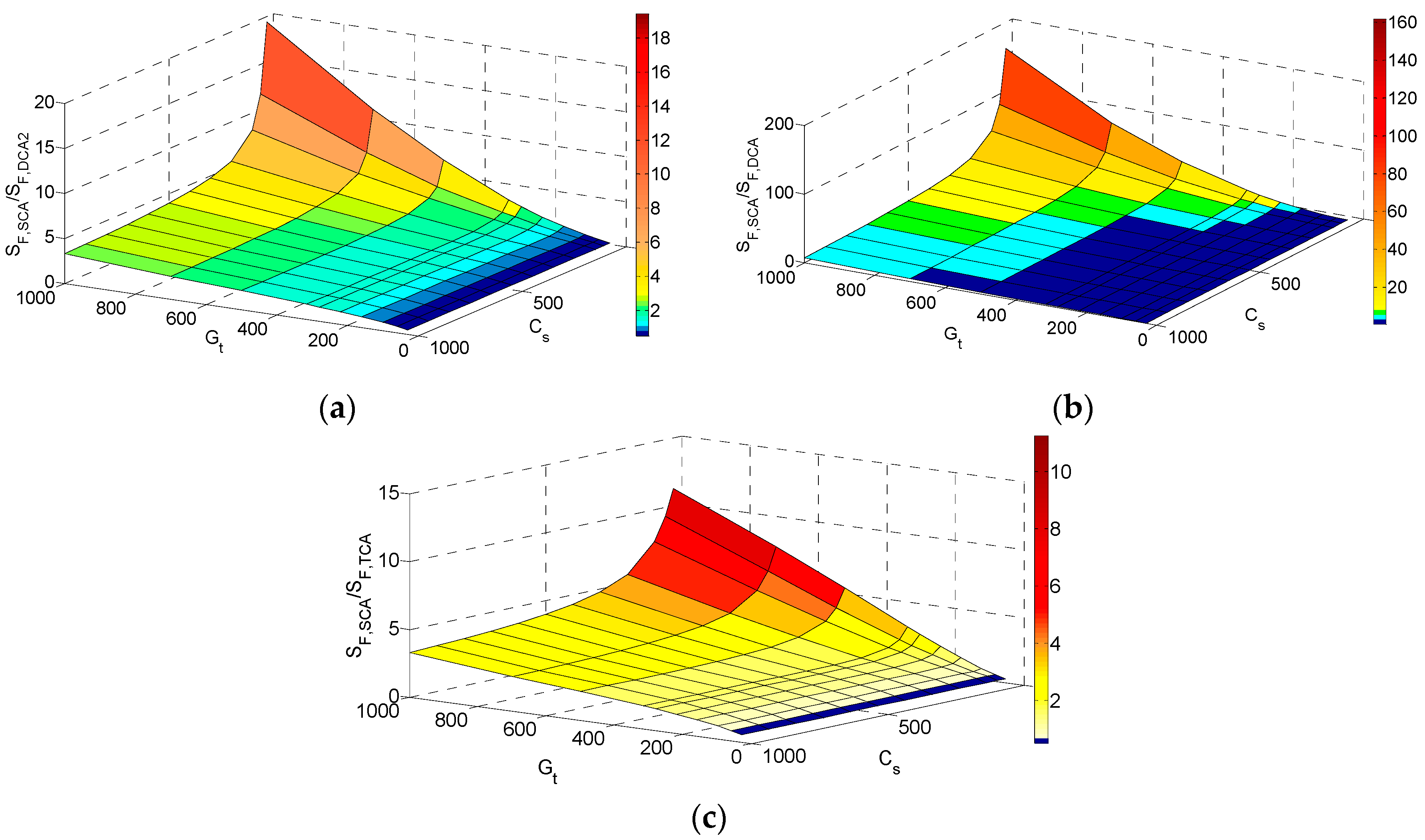
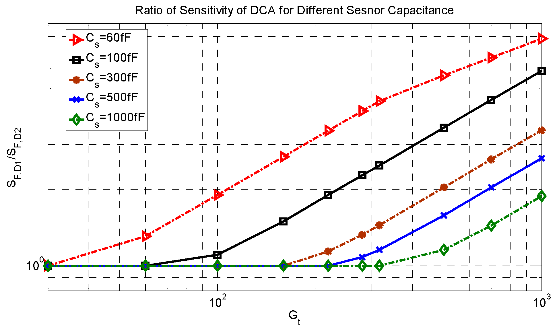
To illustrate the difference in the minimum sensitivity factor between the DCA and DCA
2, the ratio of the sensitivity factor of DCA to DCA
2 is shown in
Figure 11. Based on the sensor capacitance and the total gain, this ratio can be very different. For a small gain, this ratio is 1 because all amplification is done in the first stage. When the gain is increased, this ratio is increased and becomes larger for a smaller sensor capacitance. This is because the DCA can be designed to have an insignificant loading factor, which is important in systems that require a high gain and have a small sensor capacitance.


