Article

A Low-Power CMOS Piezoelectric Transducer Based Energy Harvesting Circuit for Wearable Sensors for Medical Applications

1
Department of Electrical Engineering and Computer Science, University of Tennessee, Knoxville, TN 37996-2250, USA
2
Department of Mechanical, Aerospace, and Biomedical Engineering, University of Tennessee, Knoxville, TN 37996-2210, USA
*
Author to whom correspondence should be addressed.
J. Low Power Electron. Appl. 2017, 7(4), 33; https://doi.org/10.3390/jlpea7040033
Submission received: 20 September 2017 / Revised: 8 December 2017 / Accepted: 12 December 2017 / Published: 18 December 2017
(This article belongs to the Special Issue Low-Power Electronic Circuits for Monolithic Smart Wireless Sensors)

Abstract

:
Piezoelectric vibration based energy harvesting systems have been widely utilized and researched as powering modules for various types of sensor systems due to their ease of integration and relatively high energy density compared to RF, thermal, and electrostatic based energy harvesting systems. In this paper, a low-power CMOS full-bridge rectifier is presented as a potential solution for an efficient energy harvesting system for piezoelectric transducers. The energy harvesting circuit consists of two n-channel MOSFETs (NMOS) and two p-channel MOSFETs (PMOS) devices implementing a full-bridge rectifier coupled with a switch control circuit based on a PMOS device driven by a comparator. With a load of 45 kΩ, the output rectifier voltage and the input piezoelectric transducer voltage are 694 mV and 703 mV, respectably, while the VOUT versus VIN conversion ratio is 98.7% with a PCE of 52.2%. The energy harvesting circuit has been designed using 130 nm standard CMOS process.

1. Introduction

Technological advancements in low-power CMOS processes have driven rapid development of sensor electronics such as implantable and wearable sensor systems. The powering of such sensor systems has remained a major problem since the traditional batteries can leak resulting in serious health problems in patients. Moreover, in typical sensor systems, the available space for batteries is very limited thereby restricting the battery capacity. Energy harvesting has emerged as one of the potential solutions for powering the sensor electronics and has been widely studied in recent years. Energy can be harvested from various ambient energy sources such as electromagnetic, wind, mechanical vibration, RF, and thermal energy etc. There are three general energy sources that utilize vibration, namely electrostatic, electromagnetic, and piezoelectric. Among these sources, the piezoelectric vibration based energy harvesting system has received a great deal of attention because of its ease of integration with electronic systems and moderate power density. Several rectifier circuits based on piezoelectric transducers have been reported in [1,2,3,4,5,6,7]. The circuits reported in [4,5,6] aim to reduce the voltage drop across rectifier diodes while references [2,3,4,5,6,7,8,9] aim to reduce the wasted charges associated with the charging of the plate capacitance of the piezoelectric transducer to further increase the overall efficiency of the systems. In [1,8,10], the researchers have used techniques called bias-flip and synchronized switch harvesting on inductor (SSHI) to improve the extraction of energy. However, the major problems associated with the schemes involve the requirement of relatively large inductors to improve the overall efficiency while still requiring very complex control circuits.

2. Piezoelectric Energy Harvester

2.1. General Architecture of Energy Harvesting System

Figure 1 shows a general building block or system architecture of a piezoelectric energy harvesting system [1,11]. A piezoelectric transducer can convert vibrational energy into electrical energy or can be used as a vibrational device by application of an electrical source such as a battery. When a piezoelectric transducer is used as an electrical energy generator, an AC voltage is produced at the output. Therefore, an AC-to-DC rectifier or an AC-to-DC converter must be constructed to acquire a useful DC output voltage. Since the energy generated by an AC-to-DC rectifier or a converter is not sufficient or stable enough to directly power up the system, the energy should be generally stored in a battery or a super capacitor followed by a regulator such as a DC-DC converter, LDO etc. In general, there are two types of conventional rectifiers: a voltage-doubler and a full-bridge rectifier [8]. The major drawbacks of these two conventional structures are usually low power extraction and low power conversion efficiencies. A low extraction efficiency is mainly attributed to charging and discharging of the internal parasitic capacitances of a piezoelectric transducer whenever it changes its polarity and the large voltage drop occurs due the diode turn-on voltage [8]. To overcome this drawback, a number of different schemes have been proposed such as synchronized switch harvesting on inductor, switch-only harvester, etc. In order to improve the conversion efficiency of a rectifier, a diode can be replaced by a CMOS circuit. A CMOS based rectifier has lower voltage drop compared to a conventional off-chip diode rectifier. In this paper, a CMOS synchronous switch based energy harvesting circuit is reported which offers several advantages over the schemes reported in literature due to its simplicity of design, moderate energy harvesting, and the requirement of no off-chip components except the output capacitor.

2.2. Transducer Modeling

A piezoelectric device can be modeled in both mechanical and electrical domains that are coupled through a magnetic coil [12], as illustrated in Figure 2a [10,12,13]. In the mechanical domain model of a piezoelectric transducer, RM represents the mechanical damping, CM is the reciprocal mechanical stiffness, and LM is the effective mass. In the electrical domain, the vibrational excitation can be modeled as a current source with a parasitic capacitance, CP and a parasitic resistance, RP. In the proposed CMOS active rectifier with a switch, a typical model of a piezoelectric device has been used. The parameter values for the piezoelectric transducer are chosen such that CP is 25 nF, RP is 1 MΩ, and IP is 45 µA.

3. CMOS Full-Wave Rectifier

3.1. Operating Principle
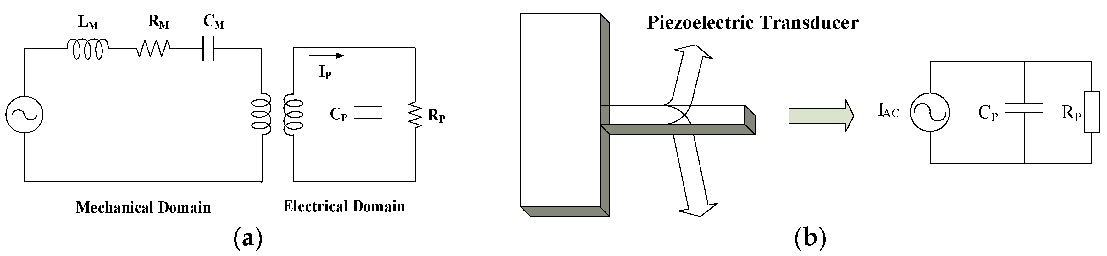
As shown in Figure 2 [8], a piezoelectric transducer can be modeled as a sinusoidal current source iP(t) = IP sin(2πfPt), in parallel with a parasitic plate capacitor, CP and a parasitic resistor, RP. The amplitude of a piezoelectric transducer current, IP varies with the mechanical excitation level of the piezoelectric transducer while fP represents the excitation frequency of the piezoelectric transducer.
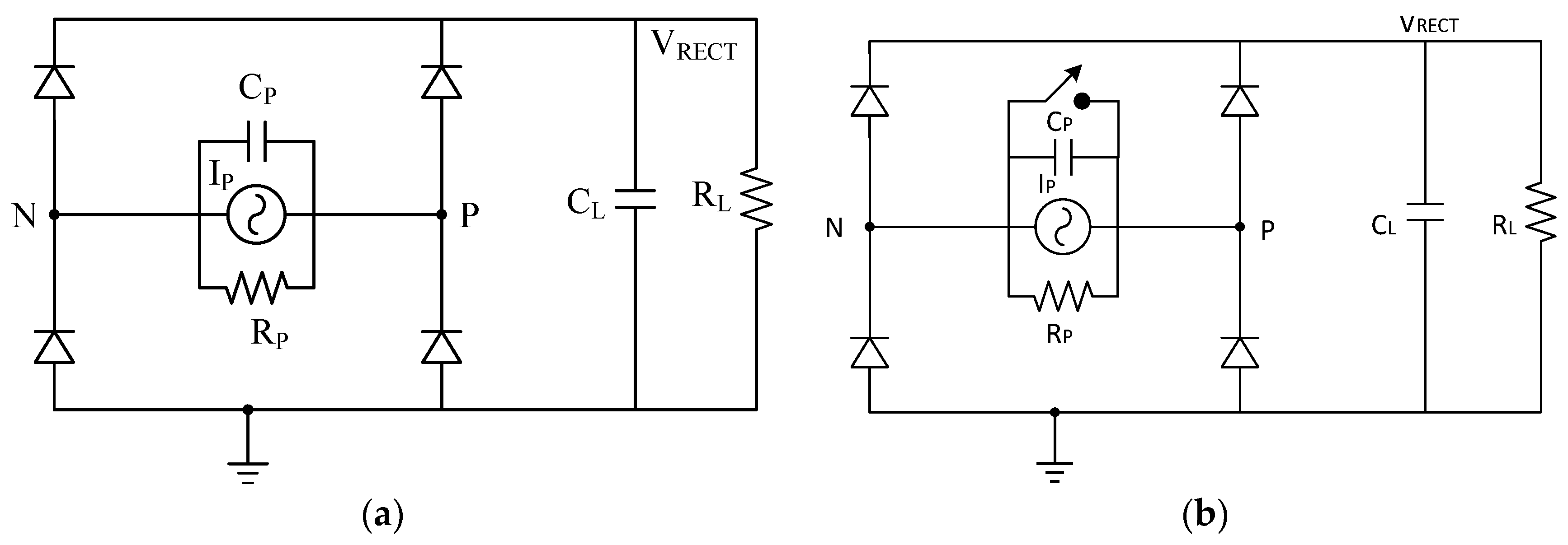
A typical full-wave bridge rectifier consists of four diodes. The major problem of using an off-chip diode in a conventional rectifier circuit is that it results in a substantial voltage drop due to the diode turn-on voltage (Vd), which is typically 0.5~0.7 V. This large turn-on voltage causes a significant loss in a conventional full-bridge rectifier. In addition, charging and discharging of the plate capacitance of a piezoelectric transducer results in a loss of available charges from the transducer. To overcome these problems, a CMOS based full-bridge rectifier with a switch-only circuit in parallel with a piezoelectric transducer is proposed in [8]. In the switch-only (SO) rectifier scheme, a switch is turned on whenever the transducer current crosses a zero which helps discharge the capacitor, CP. Unlike a conventional rectifier, this process allows the SO rectifier not to discharge from (VRECT + 2Vd). 
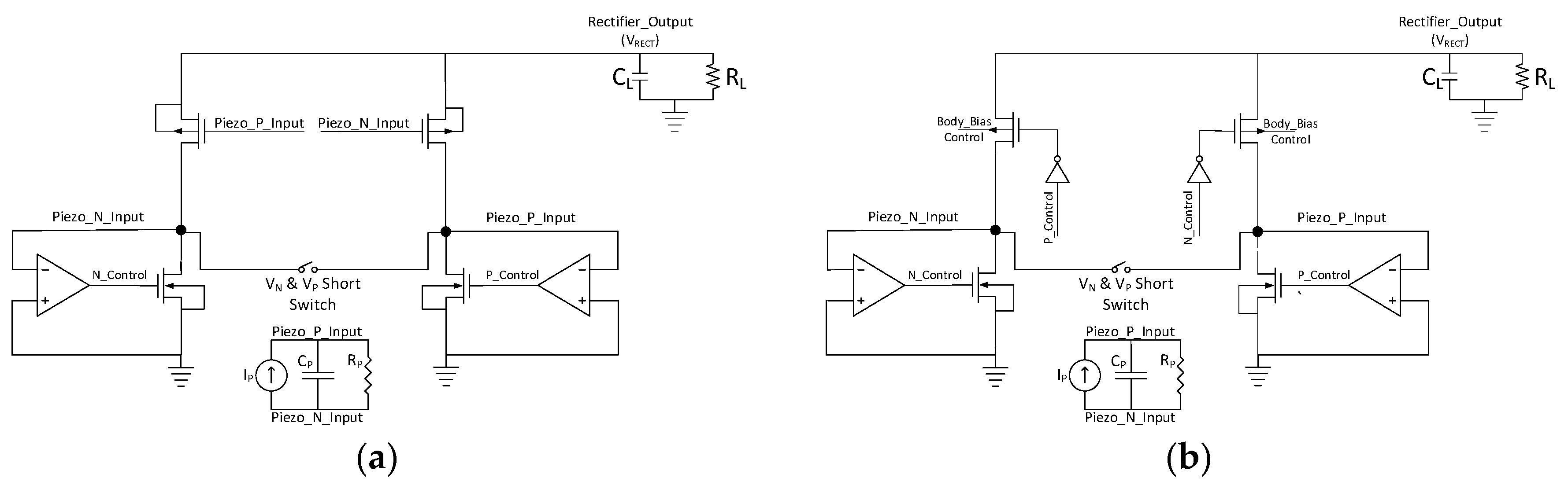
Figure 3a,b show a conventional full-bridge rectifier and a rectifier with switch-only scheme, respectively. To reduce the voltage-drop across a diode which affects the conversion efficiency, a CMOS based full-wave bridge rectifier with a switch is presented in this paper. The advantages of this proposed design include the ability to power the proposed circuit to operate without requiring any off-chip components even though the power generated by the SO rectifier is less than that of the bias-flip or other power enhanced structures. This allows more flexibility to integrate the circuits with an integrated system. In addition, by using a separate control signal for the PMOS switch in a SO rectifier, the current for charging and discharging of Csg of the PMOS device can be effectively reduced, which increases the available energy transfer time to the output load. In addition, a switch can be added in between VN and VP inputs of a piezoelectric transducer to reduce the wasted charges which is used to charge or to discharge the parasitic capacitance of a piezoelectric device. Figure 4 shows the circuit diagram of the proposed circuit as well as the system reported in [1,3,8].

3.2. Proposed Active Full-Wave Rectifier

Figure 4a shows the full-wave rectifier structure reported in [1,3,8]. Due to the cross-coupled nature of the circuit, it requires a current and time to charge and discharge Csg of the PMOS switch charged by a piezoelectric transducer directly prior to being turned on and off. Therefore, to turn on the PMOS switch in order to charge Csg the input voltage from a piezoelectric transducer, VPN should be greater than |Vthp|. Therefore, the available transfer time of energy from a piezoelectric transducer will be reduced because of the time required to charge Csg.
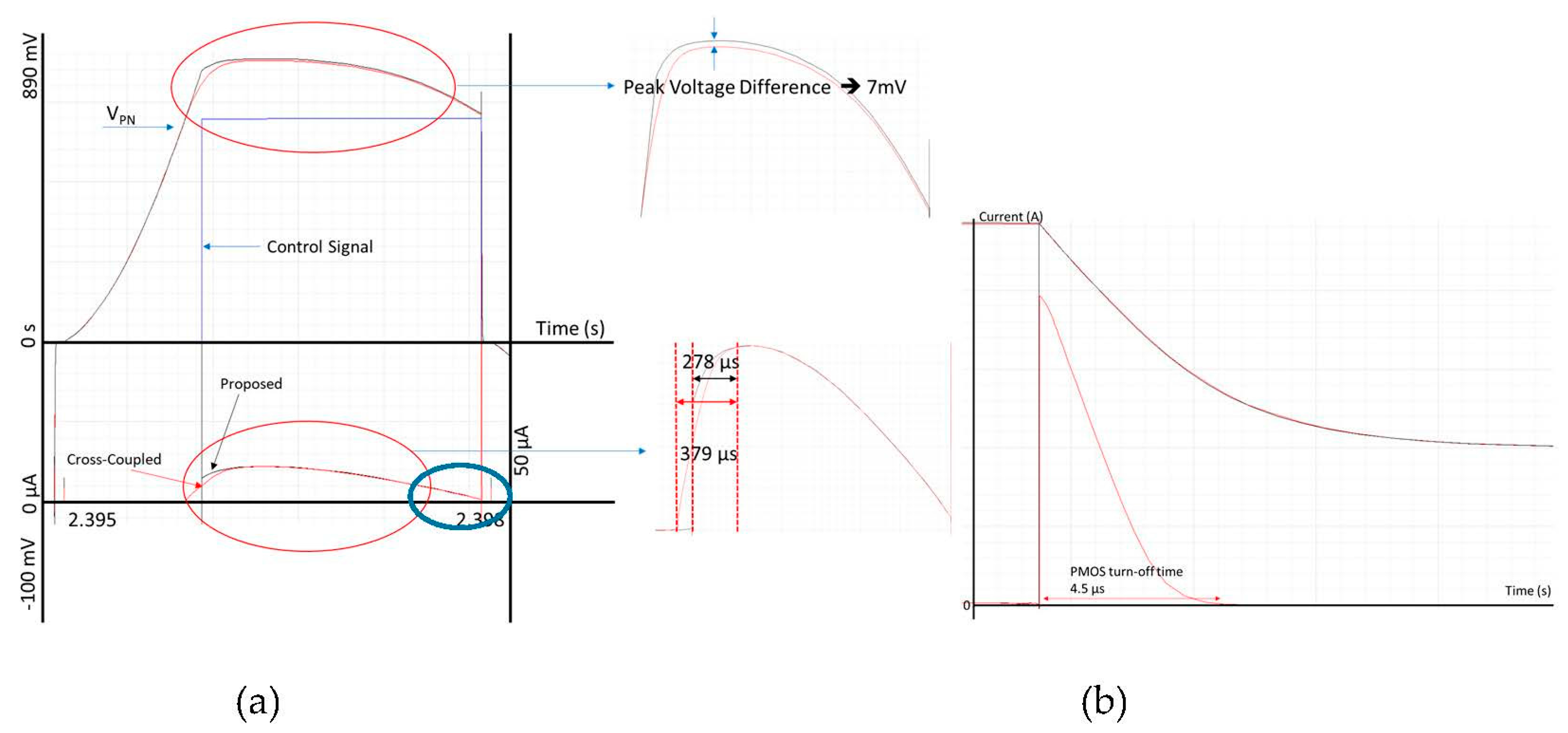
However, in the proposed active rectifier circuit as shown in Figure 4b, the PMOS on/off are controlled by the NMOS turning on/off signal and are driven by output voltage powered buffer. Therefore, the proposed system does not pose problems associated with the design reported in [1,3,8]. As shown in Figure 5, the time required to charge Csg is about 100 µs (about 39% less time to reach the peak current from a piezoelectric transducer) less than cross-coupled system presented in [1,2,8]. The PMOS off-time also has been reduced as shown in Figure 5b. The proposed system instantly discharges Csg, and as a result, the off time is in the nano-second range even though the off-time of the cross-coupled system is 4.5 µs. Therefore, more energy from a piezoelectric transducer can be transferred to the output resulting in the VPN voltage ([VP-VN] of a piezoelectric input voltage) being about 0.7% higher than that of a cross-coupled based active rectifier with the same load and piezo input. Although 0.7% can be considered as a small improvement in a system, for low input power systems such as the one proposed in this paper, every available energy should be squeezed so that more available energy can be transferred to the output. In addition, if the excitation frequency as well the force applied to a piezoelectric transducer are lowered, then, charging time will be increased because of less available charges from a piezoelectric transducer. As a result, the voltage amplitude of VPN will be lowered so as VRECT. In addition, since the proposed energy harvesting system can handle more energy than a cross-coupled rectifier, the output voltage, VRECT, is higher than that of the cross-coupled circuit. 
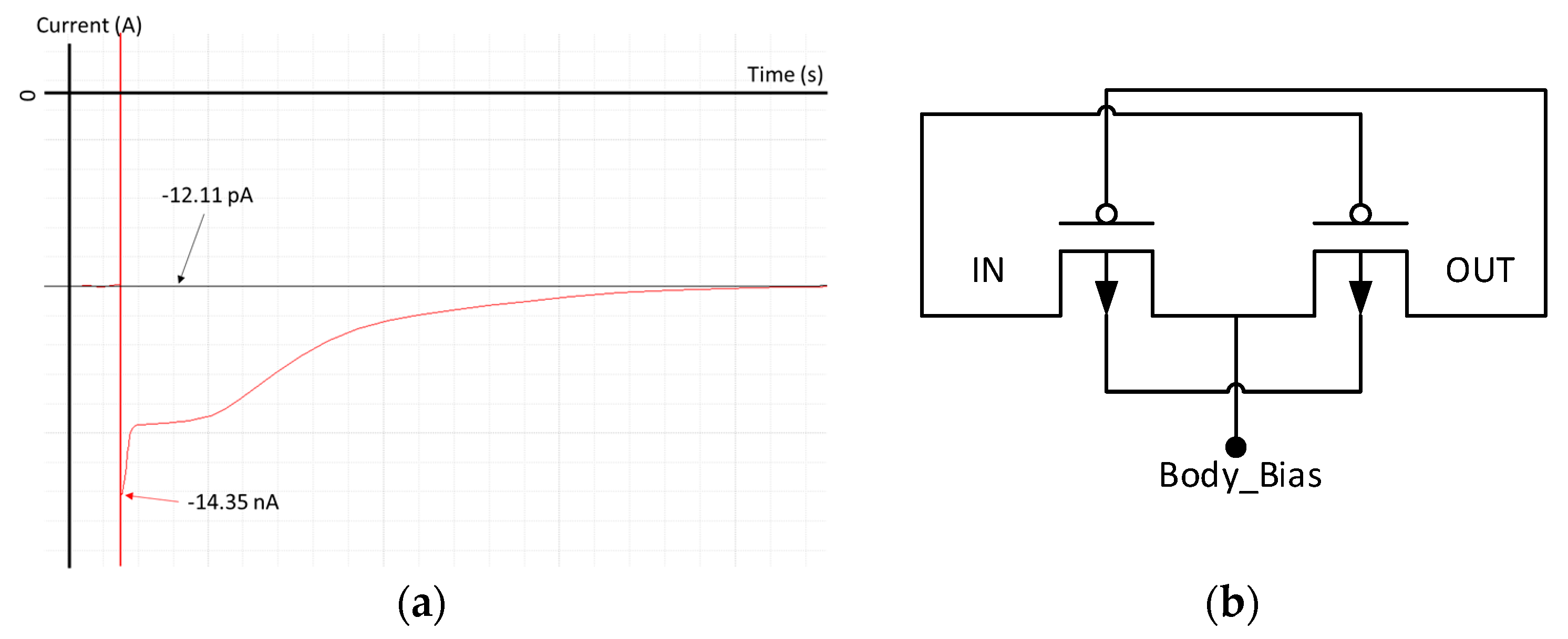
Figure 6a,b show the body leakage current and the body bias control circuit utilizing the leakage current, respectively. With the help of simple implementation of body-bias control circuit, the proposed system can achieve lower body leakage current compared with cross-coupled system reported in [1,3,8].
Figure 6 shows the body leakage current of the circuit that has been used to control the body bias. In Figure 6b, IN is connected to the VRECT, OUT is connected either VP or VN, and the body-bias port is connected to the body of the PMOS switch. As shown in Figure 6a, the leakage current in the proposed system is −12.11 pA (black line) while the leakage current in cross-coupled system is −14.35 nA (red line), which is a huge improvement. With the help of all the above improvements, the output voltage from a proposed active rectifier is 698 mV while that of the rectifier with cross-coupled based is 694 mV.
The proposed switch-only active rectifier as well as the cross-coupled active rectifier with switch-only are simulated with the same MOSFET sizes as well as the same input piezo current. The only difference between the two schemes is the top PMOS gate control methods. 
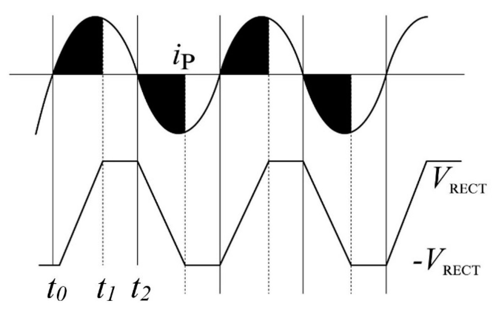
Figure 7 shows the waveform of the piezoelectric transducer current, iP versus VRECT of a conventional full-wave rectifier. The shaded regions show the wasted energy due to charging and discharging of a parasitic capacitor, CP.
It is evident from the figure that a significant amount of energy is lost due to the charging and discharging actions of CP. In Figure 7, the difference between t0 to t1 represents the wasted energy when iP is used to charge CP. The total charge available in full-bridge rectifier can be written as,
Q t o t a l / c y c l e = 0 2 π / ω P i P d t = 4 I P ω P = 4 C P V P
where Vp is the amplitude of the open circuit voltage of the piezoelectric transducer.
The piezoelectric transducer current, iP, has to charge CP from VRECT to −VRECT in every cycle before turning on a diode in a conventional full bridge diode. Therefore, charge lost in every cycle can be written as [8],
Q l o s t c y c l e = 2 C P ( V R E C T ( V R E C T ) ) = 4 C P V R E C T
From Equations (1) and (2), the actual charge that used to charge CL in Figure 3 can be written as [8],
Q R E C T c y c l e = Q t o t a l c y c l e Q l o s t c y c l e = 4 C P V p 4 C P V R E C T
Multiplying Equation (3) by the output voltage of the piezoelectric transducer, VRECT provides the total energy delivered to CL. Therefore, the total energy can be written as [8],
E n e r g y R E C T c y c l e = Q R E C T c y c l e × V R E C T = 4 C P V R E C T ( V p V R E C T )
Since the piezoelectric transducer operates at a frequency, fP the total power delivered to the output capacitor, CL by the conventional full-bridge rectifier can be expressed as [8],
P o w e r R E C T = E n e r g y R E C T c y c l e × f P = 4 C P V R E C T   f P ( V p V R E C T )
Using Equation (5), the maximum available power is obtained when VRECT = VP/2, and can be expressed as
P R E C T ( M A X ) = C P ( V P ) 2 f P
To reduce this unwanted energy loss or to increase the energy transfer from a piezoelectric transducer, one effective scheme involves inserting a switch in between the inputs of the piezoelectric transducer, VP and VN as shown in Figure 4.
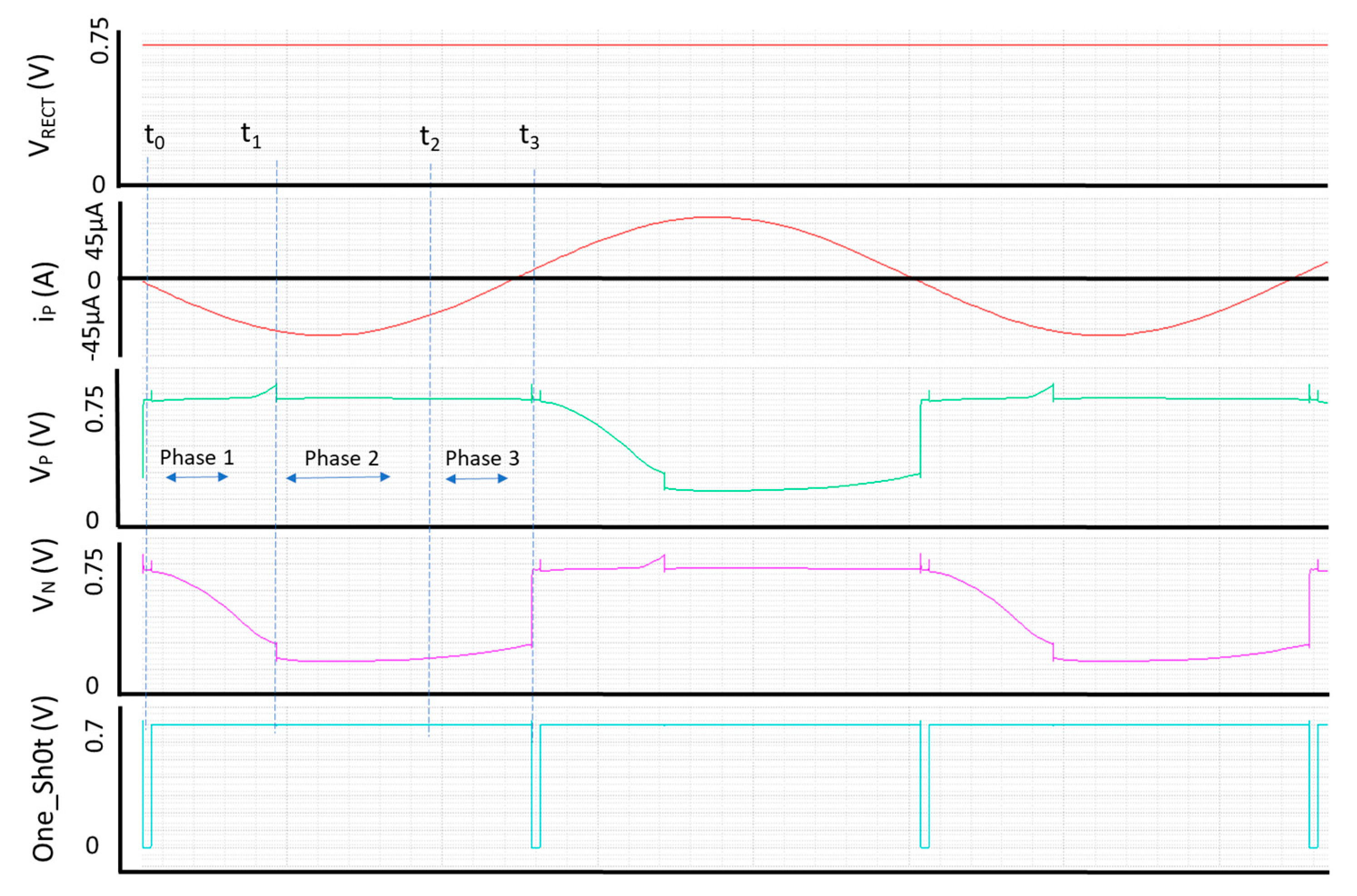
Figure 8 shows the steady-state operation of the proposed full-wave rectifier. It can be seen from Figure 8 that the operation of the proposed full-wave rectifier can be divided into three phases. In phase 1 between t0 to t1, a sinusoidal current, iP from a piezoelectric transducer starts charging a parasitic capacitor, CP. Unlike a conventional piezoelectric transducer as shown in Figure 3, time for charging of CP has been reduced significantly because of the inclusion of a switch in between VP and VN. In Figure 9, it can be seen that as the one-shot turns on, the VP and VN terminals are shorted instantly and therefore it does not have to charge from its previous value, rather it starts from zero. In a conventional rectifier, when iP is changing its polarity from positive to negative, CP should be discharged from (VRECT + 2Vd) to zero and charged from zero to −(VRECT + 2Vd). In phases 2 and 3, since the charging of a parasitic capacitor CP has been completed, the energy can be transferred to the output capacitor, CL through the full-wave rectifier.
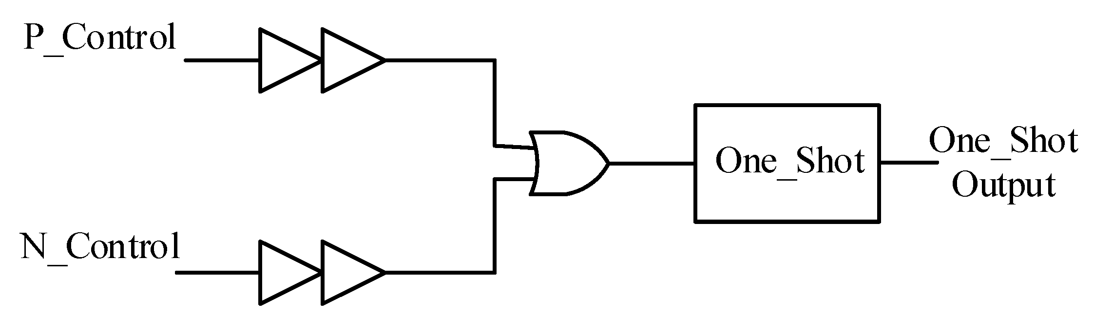
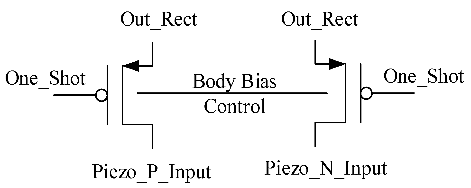
Figure 9 shows the switch inserted in between VP and VN of a piezoelectric transducer which allows the capacitor to discharge to zero. The working principle for the one-shot signal switch is very simple.
Whenever a piezoelectric transducer crosses the zero point, the one-shot control circuit as shown in Figure 10 is designed to provide a short pulse which shorts the input ports of a piezoelectric transducer to reset the voltages VP and VN. This shorting action will help improve the efficiency of the piezoelectric energy harvesting circuit by reducing a waste charge. Therefore, iP does not have to charge or discharge CP from ±(VRECT + 2Vd) but rather from zero to (VRECT + 2Vd). The bottom two NMOS switches are controlled by a low-power comparator while the top two PMOS switches are controlled by P_Control and N_Control bar signals. All the control circuits as well as the comparator are powered by the harvested supply voltage, VRECT.
In the proposed full wave rectifier, the charge lost in every cycle can be denoted by [8],
Q l o s t / c y c l e = 2 C P V R E C T
The charge available can be calculated as [8],
Q R E C T c y c l e = Q t o t a l c y c l e Q l o s t c y c l e = 4 C P V o p e n 2 C P V R E C T
Therefore, the total power delivered to the output load CL can be expressed as follow [8].
P o w e r R E C T = E n e r g y R E C T c y c l e × f P = 2 C P V R E C T   f P ( 2 V o p e n V R E C T )
Comparison of Equations (3) and (8) reveals that the charge lost is reduced by about 50%. Therefore, inserting a switch in between VP and VN of a piezoelectric transducer can save a substantial amount of energy. All the control circuits in this proposed active rectifier are powered by the output voltage, VRECT derived from the harvested energy. Figure 11 illustrates the start-up operation of the circuit. For the start-up of the rectifier operation, all the control circuits including the comparators are not working until CL is charged properly since no charge is accumulated in CL initially. As shown in Figure 11, leakage current flows through both PMOS(MP) and NMOS(MN) as the input of a piezoelectric transducer starts increasing thereby slowly charging CL. The initial charging current derived from this leakage current is in nano-ampere range. The time required to charge CL is approximately 120 µs and the resulting harvested supply power all the control circuits including the comparators. Proper working of all control signal starts at around 180 µs. CompP and CompN are the output waveform of comparators, and One-Shot is the output waveform of the One-Shot control signal. CompP and CompN are represent P_Control and N_Control signals in Figure 4b.

4. Measurement Results

Figure 12 and Figure 13a show the measured waveforms of the proposed full-wave rectifier. For the sake of simplicity and to validate the operation of the proposed circuits, the input signal was generated by a function generator with Vpk-pk voltage of 1.2 V (600 mV amplitude). The output was measured to be 580 mV with load resistor of 45 kΩ. The measurement data is slightly different from a simulated one because of the parasitic PCB board capacitance as well as the chip-package parasitics. Figure 12c,d show the test set-up. Since the proposed circuit is tested with a signal generator, the model used in this test set-up is the Norton to Thevenin equivalent of the circuit shown in Figure 13b. V1 represents the voltage signal from the signal generator with an amplitude of 0.6 V (VPK-PK is 1.2 V), R1 is 13.3 kΩ, and CP is a parasitic capacitance of a piezoelectric transducer.

5. Conclusions

Figure 14 shows the layout of the proposed full-wave CMOS rectifier and the microphotograph of the fabricated IC and Table 1 shows the summary of the system performance. The amplitude of the output voltage is 0.694 V. The simulated conversion ratio of VOUT versus VIN is 98.7%. The output power, POUT of the proposed full-wave rectifier is 10.7 µW, and the power conversion efficiency (PCE) of the system is 52.2%, and this PCE can be achieved at 45 KΩ (Max PCE). The main reason for the low PCE is due to the low available input power. The main idea of this proposed active rectifier is to reduce the off-chip components as much as possible so that this energy harvester can be easily integrated with other complex systems. In addition, the performance of the proposed system demonstrates that by reducing the time for charging and discharging of Csg of the PMOS switch, the input amplitude of a piezoelectric transducer will increase the output voltage. This process saves the wasted charges caused by CP, and the output voltage can be increased even though the increment in the input voltage amplitude is small. As shown in Table 1, the PCE of the proposed circuit is comparable to other energy harvesting circuits reported in literature. Reference [8] used an external power source, which will decrease the harvested power. References [1,3] used high piezo current, iP compared to this proposed design and high voltage amplitude to achieve higher output voltage. In addition, an inductor is used in reference [1] to further increase the PCE of the overall system. However, with such high piezoelectric current as well as with an additional inductor with a fairly big value, the PCE of their system is not far from the proposed simple but effectively controlled rectifier. The input of the proposed system was provided by a function generator instead of a piezoelectric transducer for proof of concept of the proposed rectifier circuit. The preliminary test results show that the overall system performs as expected. Figure 14 shows the proposed full-wave rectifier layout and full-chip micro-photograph.

Acknowledgments

The chip has been manufactured through the MOSIS education support.

Author Contributions

Taeho Oh designed and tested the proposed novel works. Thanks to Syed K. Islam, Mohamad Mahfouz and Gary To for their support of the test equipment as well as valuable advice for the work.

Conflicts of Interest

The authors declare no conflict of interest.

References

  1. Krihely, N.; Ben-Yaakov, S. Self-Contained Resonant Rectifier for Piezoelectric Sources under Variable Mechanical Excitation. IEEE Trans. Power Electron. 2011, 26, 612–621. [Google Scholar] [CrossRef]
  2. Din, U.; Chung, D.; Park, D.; Lee, H.; Lee, J.W. A high energy extraction self-controllable CMOS resonant rectifier circuit for piezoelectric energy scavenging system. In Proceedings of the 2014 International SoC Design Conference (ISOCC), Jeju, Korea, 3–6 November 2014; pp. 40–41. [Google Scholar]
  3. Do, X.D.; Nguyen, H.H.; Han, S.K.; Ha, D.S.; Lee, S.G. A selfpowered high-efficiency rectifier with automatic resetting of transducer capacitance in piezoelectric energy harvesting systems. IEEE Trans. Very Larg. Scale Integr. Syst. 2015, 23, 444–453. [Google Scholar] [CrossRef]
  4. Dallago, E.; Miatton, D.; Venchi, G.; Bottarel, V.; Frattini, G.; Ricotti, G.; Schipani, M. Active self supplied AC-DC converter for piezoelectric energy scavenging systems with supply independent bias. In Proceedings of the IEEE International Symposium on Circuits and Systems, Seattle, WA, USA, 18–21 May 2008; pp. 1448–1451. [Google Scholar]
  5. Guilar, N.J.; Amirtharajah, R.; Hurst, P.J. A fully-wave rectifier for interfacing with multi-phase piezoelectric energy harvesters. In Proceedings of the IEEE Solid-State Circuits Conference, Digest of Technical Papers, San Francisco, CA, USA, 3–7 February 2008; pp. 302–304. [Google Scholar]
  6. Ottman, G.K.; Hofmann, H.F.; Bhatt, A.C.; Lesieutre, G.A. Adaptive piezoelectric harvesting circuit for wireless remote power supply. IEEE Trans. Power Electron. 2002, 17, 669–676. [Google Scholar] [CrossRef]
  7. Sun, Y.; Hieu, N.H.; Jeong, C.J.; Lee, S.G. An Integrated High-Performance Active Rectifier for Piezoelectric Vibration Energy Harvesting Systems. IEEE Trans. Power Electron. 2012, 27, 623–627. [Google Scholar] [CrossRef]
  8. Ramadass, Y.K.; Chandrakasan, A.P. An efficient piezoelectric energy harvesting interface circuit using a bias-flip rectifier and shared inductor. IEEE J. Solid State Circuits 2010, 45, 189–204. [Google Scholar] [CrossRef]
  9. Sankman, J.; Ma, D. A 12 µW to 1.1 mW aim piezoelectric energy harvester for time-varying vibrations with 450nA IQ. IEEE Trans. Power Electron. 2015, 30, 632–643. [Google Scholar] [CrossRef]
  10. Lu, S.; Boussaid, F. A highly efficient P-SSHI for piezoelectric energy harvesting. IEEE Trans. Power Electron. 2015, 30, 5364–5369. [Google Scholar] [CrossRef]
  11. Yu-Yin, C.; Vasic, D.; Costa, F.; Wen-Jong, W.; Lee, C.K. Self-powered piezoelectric energy harvesting device using velocity control synchronized switching technique. In Proceedings of the 36th Annual Conference on IEEE Industrial Electronics Society (IECON 2010), Glendale, AZ, USA, 7–10 November 2010; pp. 1785–1790. [Google Scholar]
  12. Vaddi, R.; Dasgupta, S. Enhanced bias-flip rectifier with ultra-low power control for piezoelectric energy harvester in the microwatt application scenario. In Proceedings of the Asia Pacific Conference on Postgraduate Research in Microelectronics and Electronics (PrimeAsia), Hyderabad, India, 5–7 December 2012. [Google Scholar]
  13. Paradiso, J.A.; Starner, T. Energy scavenging for mobile and wireless electronics. IEEE Pervasive Comput. 2005, 4, 18–27. [Google Scholar] [CrossRef]
Figure 1. A general building block of a piezoelectric energy harvester.
Jlpea 07 00033 g001
Figure 2. (a) Modeling of a piezoelectric transducer showing mechnical to electrical domain; (b) simplified model of a piezoelectric transducer [12].
Jlpea 07 00033 g002
Figure 3. Circuit schematics of: (a) a full-wave rectifier, (b) a conventional diode full-bridge rectifier.
Jlpea 07 00033 g003
Figure 4. (a) Full-wave rectifier circuits presented in [1,3,8] and (b) the proposed architecture.
Jlpea 07 00033 g004
Figure 5. Comparison between cross-coupled full-wave rectifier circuit reported in [1,3,8] and the proposed architecture (Simulated): (a) on-time; (b) off-time of PMOS (blue circle magnified).
Jlpea 07 00033 g005
Figure 6. (a) Body bias circuit of the PMOS switch based active rectifier circuit, (b) simulated body leakage current of the body bias circuit of the PMOS switch.
Jlpea 07 00033 g006
Figure 7. Waveform of a piezoelectric transducer.
Jlpea 07 00033 g007
Figure 8. Simulated waveform of a piezoelectric transducer output.
Jlpea 07 00033 g008
Figure 9. Schematic of the piezoelectric transducer switch.
Jlpea 07 00033 g009
Figure 10. Schematic of the one-shot digital control circuit.
Jlpea 07 00033 g010
Figure 11. Simulated start-up of the proposed active rectifier.
Jlpea 07 00033 g011
Figure 12. Measured input and output voltage waveforms of the rectifier (a) magnified; (b) full waveform.
Jlpea 07 00033 g012
Figure 13. (a) One-shot and input voltage waveforms; (b) input equivalent circuit of a piezoelectric transducer; (c) test setup; and (d) printed circuit board (PCB) implementation of the test board.
Jlpea 07 00033 g013
Figure 14. Layout and chip microphotograph of the proposed full-wave rectifier (540 µm × 540 µm).
Jlpea 07 00033 g014
Table 1. Performance Comparison.
Publications[1][3]SO [8]This Work
Inductor and External ComponentsYesNoNoNo
External PowerYesNoNoNo
Amplitude of IP by PD or Applied force2 mA94 µA3.35 g45 µA
Parasitic Capacitance of PD (nF)330251225
Vibration Frequency (Hz)185200225200
VIN,Peak3.532.40.704
VOUT (V)3.342.920.694
RL (KΩ)3.511007545
PCE (%)160% higher than conventional rectifier.
Converted PCE is 63%
-5352.2

