1. Introduction
Connected component analysis (CCA) is one of the most fundamental steps in image processing [
1]. It is widely used in several application fields, such as pattern recognition, obstacle detection, and machine learning. CCA processes the output data coming from low-level algorithms, such as binary segmentation, and provides abstract input data to other high-level processing, such as recognition algorithms [
2]. The CCA is the combination of two computations: connected component labeling (CCL) and features computation (FC). CCL algorithms distinguish different objects in the source image by assigning a unique label to all pixels that refer to the same object [
3]. Then, the FC transforms the labeled image into synthetic data, useful for the subsequent processing.
The CCL process is based on scanning the input binary image and labeling each foreground non-zero pixel in comparison to the values of its neighboring pixels. It is one of the most time-consuming tasks in CCA and, for this reason, a pure software implementation often is insufficient for the strict performance requirement for real-time elaboration. To address this issue, in the last few years, designers have directed their efforts towards the design of hardware modules for use in specialized image processing architectures. Unfortunately, most of the previously demonstrated hardware designs are suitable for a particular application environment, thus, a generally valid solution for embedded systems designs is still missing. In such integrated systems, several custom processing modules operate concurrently, they access external memory resources through several Direct Memory Access (DMA) cores, and one or more microprocessor units orchestrate their activities.
In this paper, we propose an efficient architecture for the hardware implementation of the CCL specifically designed for the inclusion in FPGA-based image processing embedded systems. The main idea of the novel approach is to overlap the most time-consuming step of the CCL algorithm, namely the label collisions resolution, and the DMA cores configuration actions that have to be performed by the ARM processors. Thus, multiple scans of the input image or any other steps limiting the frame rate of the whole system are avoided. The proposed design has been implemented on a Zynq AP-SOC 7045 chip and it reaches a 220 Mpixels/sec throughput rate. When the 640 × 480 input image resolution is chosen, a frame rate higher than 700 fps is achieved, thus significantly outperforming competitor architectures.
2. Background
The objective of the CCL is to mark all the pixels belonging to an object, also called a connected component, with the same label in the source image. In order to do this, the algorithm scans the input binary image in raster order and decides how to label each foreground non-zero pixel on the basis of the labels already assigned to the pixels within a chosen neighborhood. Typically, neighborhoods consisting of four or eight pixels are used. In these cases, two foreground pixels
p and
q are said to be 8-connected (4-connected) if there is a path consisting of foreground pixels
a1,
a2, …,
an such that
a1 = p and
an = q and, for all pixels, 1 ≤
i ≤
n − 1 and
ai and
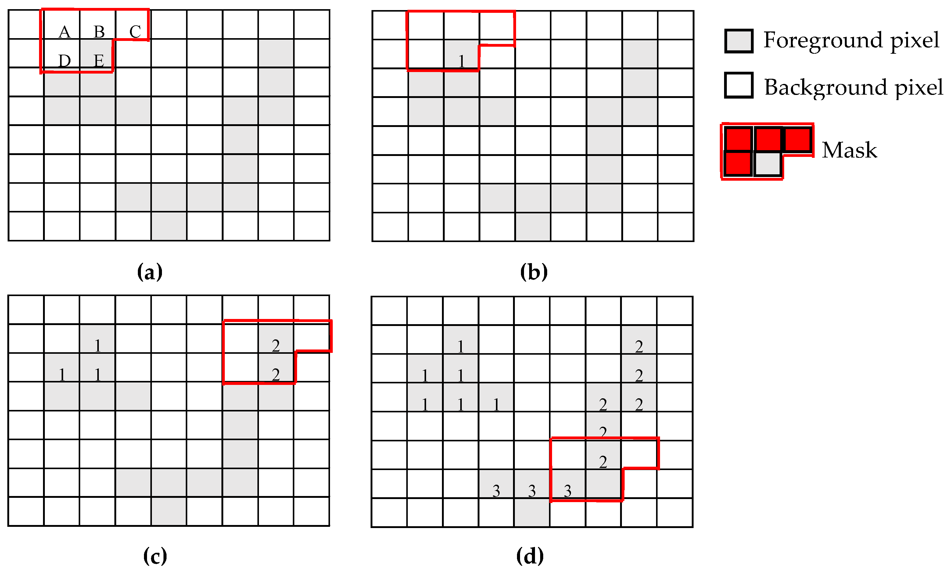
ai+1 are 8-neighbors (4-neighbors) for each other. The example reported in
Figure 1a shows the case in which the mask used allows the selection of pixels A, B, C, and D as the neighborhood of the foreground pixel E, which is being labeled. To perform the CCL over the whole image considered in the example, it is scanned in raster order. As shown in
Figure 1b, the new label 1 is assigned to the first encountered foreground pixel since its neighborhood, consisting of only background pixels, does not provide information about a possible connected component previously identified. Conversely, the foreground pixel in the mask highlighted in
Figure 1c inherits the label 2 from its neighborhood, so that now it belongs to the same connected component. During the image scan, a third condition can occur: the so called label collision or equivalence. This critical event happens when the current neighborhood contains two differently labeled pixels, as illustrated in
Figure 1d. This means that all the pixels already marked with the labels 2 and 3, and thought to belong to separate objects, instead belong to sub-portions of the same object. Therefore, all those pixels must be assigned the same label.
Resolving the chains of label collisions is the main challenge in all CCL algorithms. Usually, one of the following strategies is adopted [
4]:
Label-equivalence: in a first image scan, provisional labels are assigned to each pixel, following the criteria described in the above example. All label collisions are stored. After the first scan is completed, label collisions are resolved by finding a representative label for each group of equivalent labels for which collisions were detected. Then, each pixel of the input image can be correctly re-labeled.
Label-propagation: the first unlabeled foreground pixel is found and a new label is assigned. Then, such label is propagated to all foreground pixels connected to it. This technique requires multiple scans of the input images and/or accessing the pixels in an irregular order depending on the shapes of connected components.
Unfortunately, due to their irregular access to image pixels, label-propagation methods are not suitable for pipelined and hardware implementations. For this reason, in the following sections, the attention is focused on CCL algorithms that resolve collisions by exploiting the label-equivalence approaches.
3. Related Works
CCL algorithms based on the label-equivalence technique can be classified into several categories depending on the number of performed scans [
5]. Multi-scan algorithms perform a first forward raster scan of the input image, assigning provisional labels to each foreground pixel based on its neighborhood. When a collision occurs, the current pixel is labeled with the lowest label in the mask, without storing any equivalence. In the next stages, multiple forward and backward raster scans are alternated of the resulting image, in order to solve all the collisions generated in the first scan. The number of scans depends on the shape of the connected components in the input image. However, when an
N ×
N image is processed (with
N being the number of rows and columns of pixels in the image), the worst chain of equivalences between all the assigned labels can be resolved performing
N-1 scans. Due to this, as deeply discussed in [
6,
7], FPGA architectures designed for this approach do not reach speed performances suitable for high performance applications.
3.1. Two-Scan Algorithms
The classic CCL algorithm exploiting the two-scan approach to resolve label collisions [
8] performs a first forward scan in order to assign provisional labels to all foreground pixels and stores the collisions information in a table. The latter is typically a look-up-table in which the label and its root are kept. The second forward scan occurs to solve the collisions by reading the table of equivalences. Besides the need for two full image scans in such a scenario, label equivalences may be stored multiple times in the table, thus affecting the achievable overall performance. Recently, to speed-up the hardware implementation of the classic two-scan CCL algorithm, several strategies have been investigated [
9,
10,
11,
12,
13,
14], each having its own strengths and weakness. The architecture presented in [
9] exhibits a relatively low latency, but it was specifically designed and optimized to work only on a particular class of objects, called k-concave. Moreover, it uses two buffers to store a sub-image of the input frame on which a three-step process is performed to provide labels. The design proposed in [
10] minimizes the amount of memory required to store equivalent labels by working on a run-length encoding representation of the input binary image. However, this approach also requires additional pre- and post-processing operations, which adversely affect the latency [
11]. In order to introduce a high parallelism level, thus increasing the achievable speed performance, the strategy proposed in [
12] partitions the input image into equally sized patches. Then, a local provisional label assignment is applied in parallel to each patch during the first scan, and a local set of equivalences is generated. Finally, a fusion step occurs to merge in parallel all the sets of local equivalences. Unfortunately, as a drawback, the architecture proposed in [
12] requires large memory resources. As an example, when 720p frames must be labeled, 9846 Kbits are required, thus limiting the implementation of further processing in the case of an embedded system.
It is worth noting that the mask used to define the neighborhood of the generic foreground pixel being labeled can influence the achievable overall performance. In fact, it determines the number of accesses to the equivalence table to write/read the collisions. For instance, in [
13,
14], an extended neighborhood composed of five 2 × 2 blocks of pixels is used. The label assignment is then performed through a decision tree. For this particular mask, the pixels in the neighborhood are accessed multiple times during the scan phase since the same strategy is iterated for each foreground pixel in the input image.
To complete the CCA process, whatever CCL algorithm has been adopted, the additional computational step for FC is required to extract the features of interest of the objects in the input image, such as boundaries, position, center of gravity, etc.
3.2. One-Scan Algorithms
Often, the above mentioned features of interest are sufficient to proceed with subsequent elaboration. In such cases, CCL is not needed and the one-scan approaches, specifically developed for data streaming applications [
15,
16,
17,
18], can be efficiently adopted. These algorithms perform the FC step without either storing or calculating the labeled images.
In [
16], a one-scan architecture that also extracts the Center of Gravity (COG) of the labeled object was demonstrated. When a label collision occurs, equivalent labels are stored into a table implemented on internal block RAMs. However, resolving the complex chains of equivalences is frame-interleaved with the labeling process, thus significantly reducing the frame rate of the whole system. A hybrid hardware-software implementation of a single-scan algorithm for features extraction was presented in [
17]. In that implementation, a DRAM is used to store the initially labeled image, and block RAM buffers are used to temporarily store a label-connection table and a data table. In order to make the insertion of new features to be extracted more flexible, but to limit the overall performance in practical environments, the ARM-based processor is instead used to update the tables. The run-length-based approach is also investigated for one-scan methods to extract statistical information of connected components in a binary image [
18]. In such a work, two adjacent rows of the input image are simultaneously processed to generate runs for the current row and indexes of equivalent runs with respect to the previous row. Statistical information between equivalent runs in adjacent rows are merged to extract the features of interest for the whole image, including boundary pixel coordinates, accumulated value of horizontal and vertical coordinates, and number of pixels in a region. Therefore, in order to identify complete connected regions, this information has to be further processed.
This work proposes a solution suitable for hardware implementation of the CCL process in modern heterogeneous FPGA SoCs. Compared with two-scan methods discussed in
Section 3.1, our proposal performs the CCL in one scan, resolving on the fly the collisions when the provisional labeled image is transferred for the next elaboration. In such a way, the performance achievable by the overall video processing system is significantly improved. Since the FC step can run concurrently to the CCL, a system designed as described here allows a complete CCA process to be performed by scanning the input image just one time.
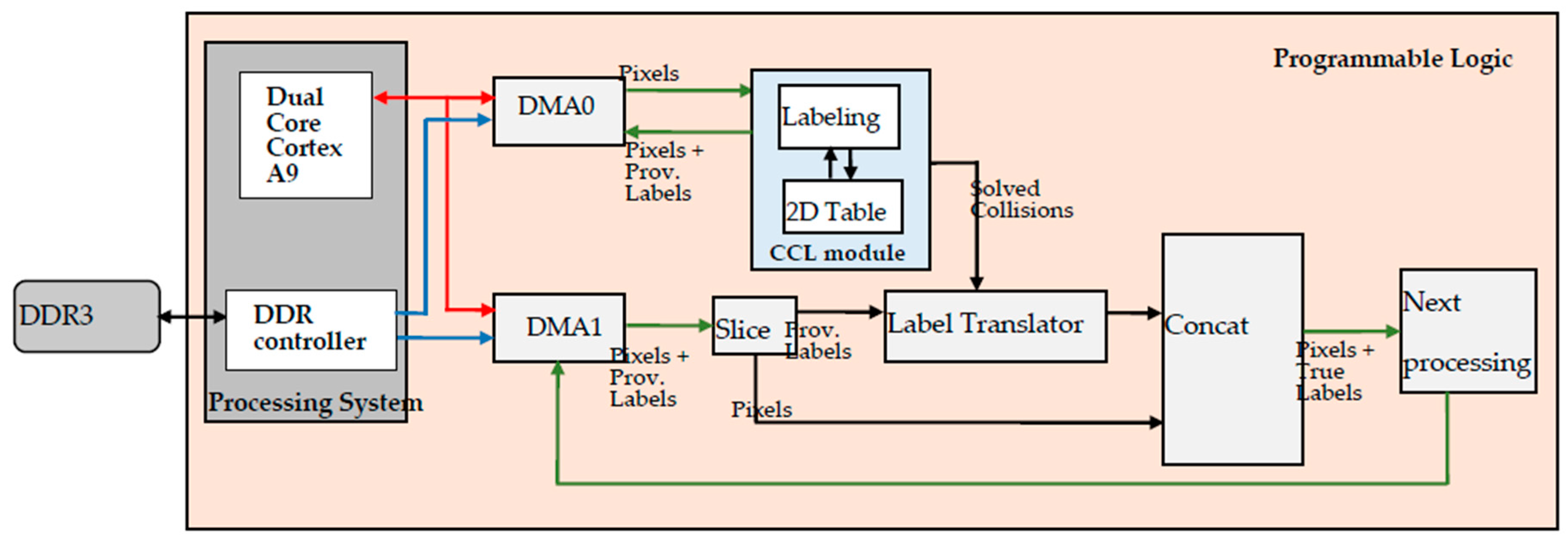
4. The Proposed Architecture
The proposed CCL architecture was designed by taking into account that it will be used as a component of a complex system architecture realized on a System-On-Chip. We refer to the Xilinx Zynq-7000 AP-SOC, but our design can be easily accommodated in all FPGA platforms with either a soft-core processor or dedicate controller to manage the operational flow and DMA transfers [
19].
In
Figure 2, the system architecture exploiting the novel CCL module is illustrated. The dual-core ARM Cortex-A9 processor communicates with blocks in the SOC through AXI4 interconnection [
19]. In the less favorable scenario, the ARM processors are exclusively used to configure the DMA cores through AXI4-Lite interfaces; in other words, the processor sends to the DMAs the external memory addresses to be used in the transfers and all other information to complete the transactions [
19].
In the system architecture of
Figure 2, only two DMAs are depicted, and all other devices needed to capture the source images from a camera, to perform the binary segmentation, and to store the resulting binary image into the external DDR memory are omitted for clarity. DMA
0 is configured to read from the external memory the binary pixels by means of a
Memory Mapped transaction, and it forms a continuous stream of pixels on its
MM2S AXI4-Stream (AXIS) interface [
20]. Such a stream is inputted to the CCL module and, with a latency of two clock cycles, an output stream is provided in which each data packet contains the original pixel plus a provisional label computed by the CCL module. Such an output stream is sent to the
S2MM interface of DMA
0 to be written in the external memory.
Further, to assign the provisional label to each foreground pixel of the input binary image, the CCL module stores label collisions in a 2D table, organized as a register file. When the last pixel in the frame is processed, the resolution of all label collisions automatically starts. Contemporaneously, DMA0 sends an interrupt to the ARM cores to inform that the labeled image is now available in the external memory and the subsequent processing can start, in other words, DMA1 can be configured to transfer the provisionally labeled image to the Next Processing block for further elaboration.
The collisions resolution phase and the configuration of DMA1 occur in parallel, thus, the time needed to update the 2D table is totally or partially hidden by the execution of the portion of the software code running on the ARM processors to start any subsequent processes.
When all collisions are resolved, the CCL module writes its results in a Look-Up-Table (LUT), acting as a Label-Translator, and flags the resolution completion. Then, DMA1 reads from the memory the provisionally labeled image, but data on its MM2S AXIS bus is sliced so that the provisional label is firstly converted by the Label-Translator LUT before it is actually delivered to the subsequent processing stage.
The use of 2D binary tables in the resolution of conflicting events was also adopted in disparate environments [
21]. There, a 2D Dependence Matrices Table was used to realize an efficient instruction scheduler for dynamic ALU cascading. However, due to the very different nature of the information stored in the 2D table, both the storing criterion and the table update phase follow a completely distinct algorithm with respect to our proposal.
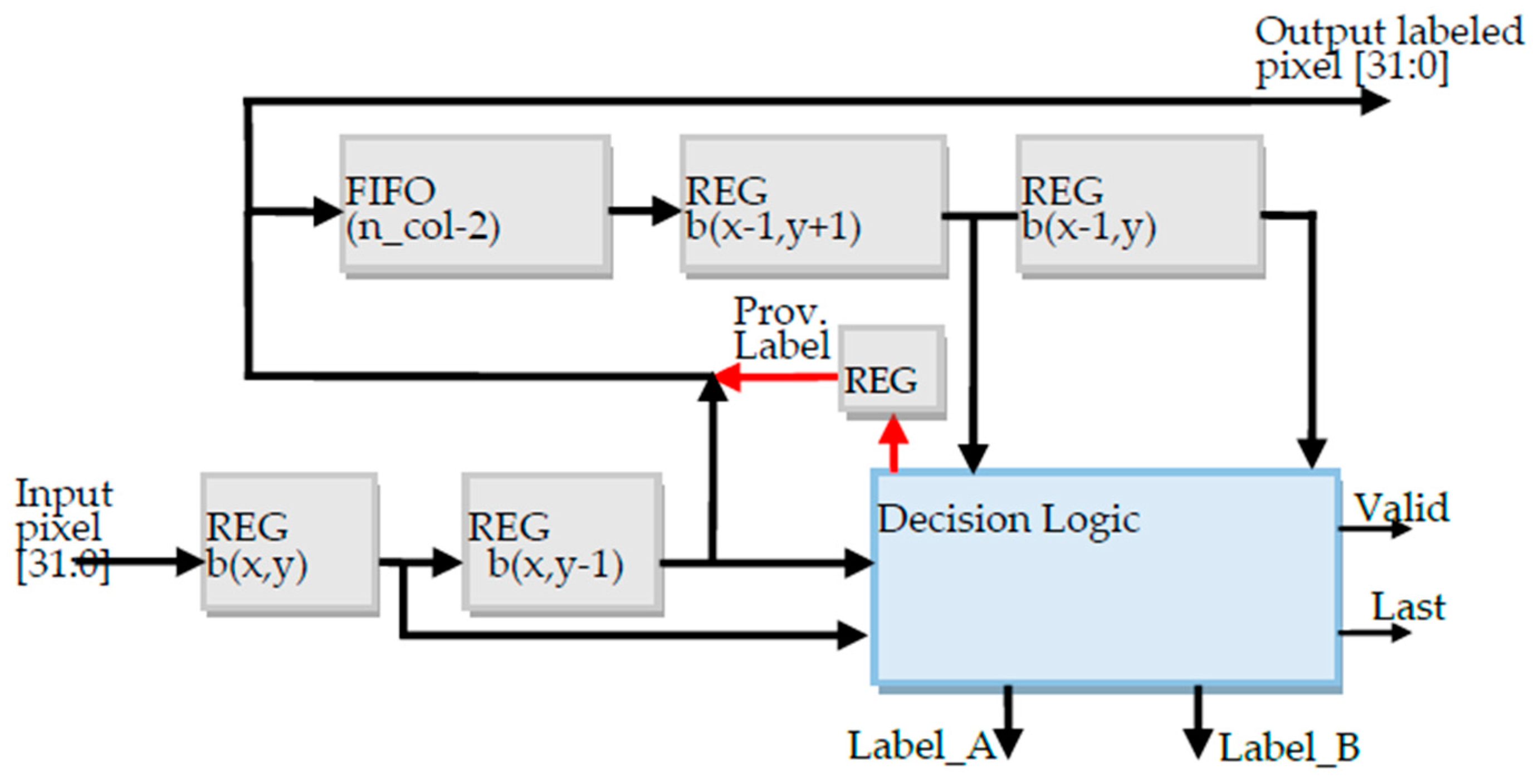
4.1. Provisional Labeling Circuit
All the custom modules detailed below have been described by means of parametric VHDL codes. The
Provisional Labeling circuit illustrated in
Figure 3 receives the stream of binary pixels coming from the 32-bit AXIS DMA
0 interface; it forms the chosen pixels neighborhood and assigns the provisional label to the current pixel
b(
x,
y). Finally, it merges pixel and label information on the output 32-bit stream. The circuit has been equipped with custom input-output standard AXIS interfaces that are not depicted in
Figure 3. A FIFO stage, whose depth is related to the width resolution of the input image, is used to form the pixel’s neighborhood.
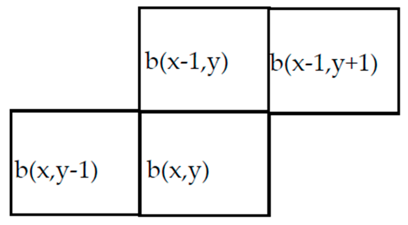
Without loss of generality, we have chosen the neighboring pixels
b(
x,
y − 1),
b(
x − 1,
y + 1) and
b(
x − 1,
y), as shown in
Figure 4. When a new pixel enters the pipeline, the chosen neighborhood is transferred to a logic circuit that assigns the provisional label based on the following rules:
If the current pixel is a foreground pixel and its neighborhood contains only background pixels, a new label is assigned to the current pixel b(x,y). New labels are generated in ascending order.
If the neighborhood contains only a labeled foreground pixel, b(x,y) inherits the label associated with such pixel.
If the neighborhood contains two foreground pixels associated to different labels, then a collision occurs. In such a case, the smallest label is assigned to the current pixel. It is worth noting that three label collisions cannot occur in the neighborhood.
The
Decision Logic circuit visible in
Figure 3 merges pixels and assigned labels with a latency of only two clock cycles. Furthermore, it stores the assigned labels and collisions in the above mentioned 2D table. As shown in
Figure 3, to this purpose,
Label_A and
Label_B signals are used. If a new label has been assigned
Label_A =
Label_B, otherwise if a collision occurs, the above signals correspon to one of the two colliding labels. Data on
Label_A and
Label_B buses are valid when the
Valid signal is asserted. Whereas, the
Last signal informs the 2D register file that the last pixel of the frame has been processed and the collision resolution phase can start.
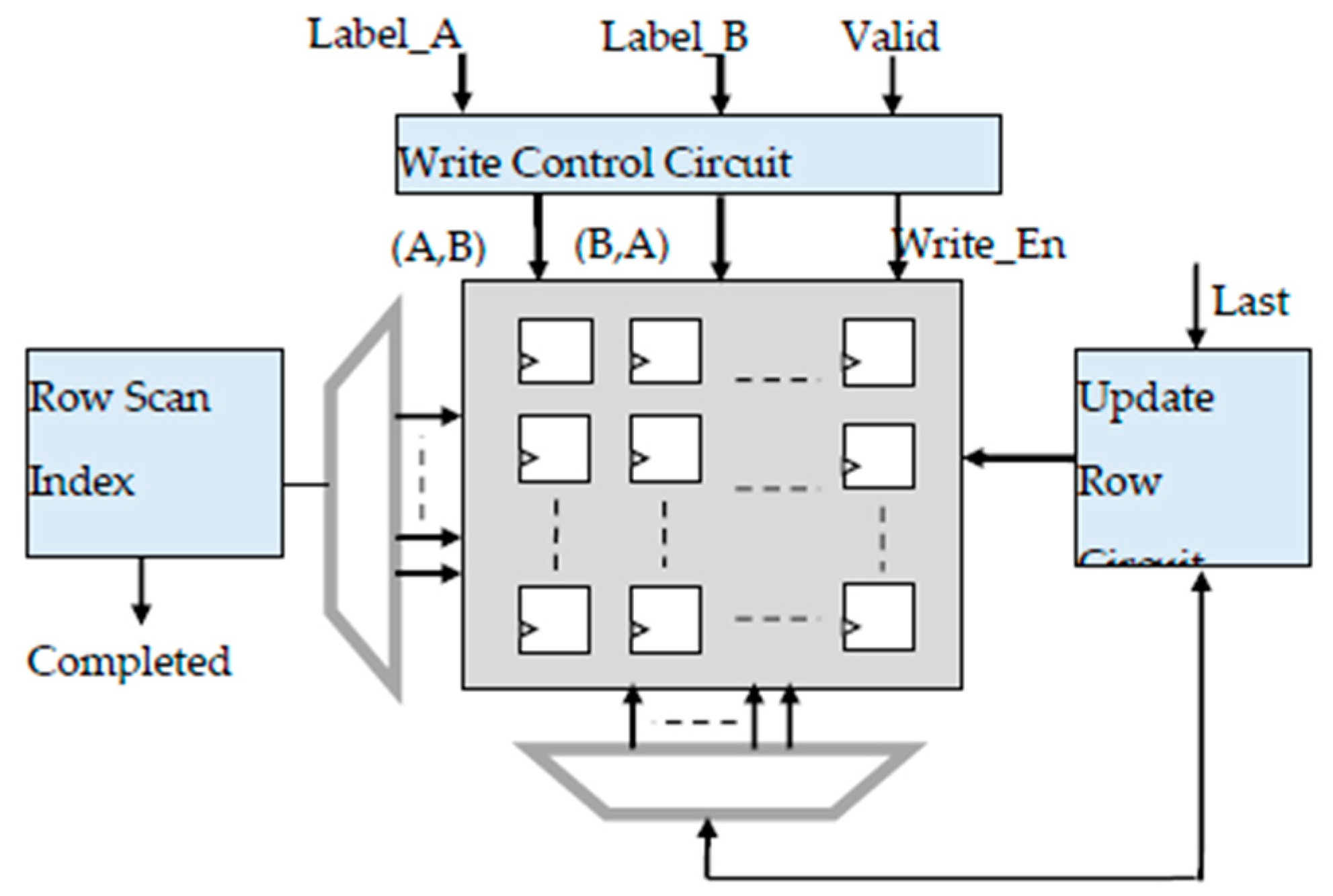
4.2. 2D Table for Resolving Label Collisions
The 2D table used for storing labels and resolving collisions is implemented as a register file with updating capability. In our implementation, it consists of NL × NL flip-flops, where NL is the number of usable labels. However, it can be easily implemented by using Block-RAMs, thus reducing slice-resources utilization, but slightly increasing latency.
In
Figure 5, the schematic diagram of the 2D table sub-system is illustrated. It consists of a
Write Control Circuit that receives information to be stored from the previous stage labels.
Label_A and
Label_B values are used as the coordinates for the access to the 2D table, so that a logic of one is written in the (
A,
B) and (
B,
A) positions at the same time. If
Label_A =
Label_B, a single write operation in a diagonal element is performed to flag that the new label has been assigned to a pixel.
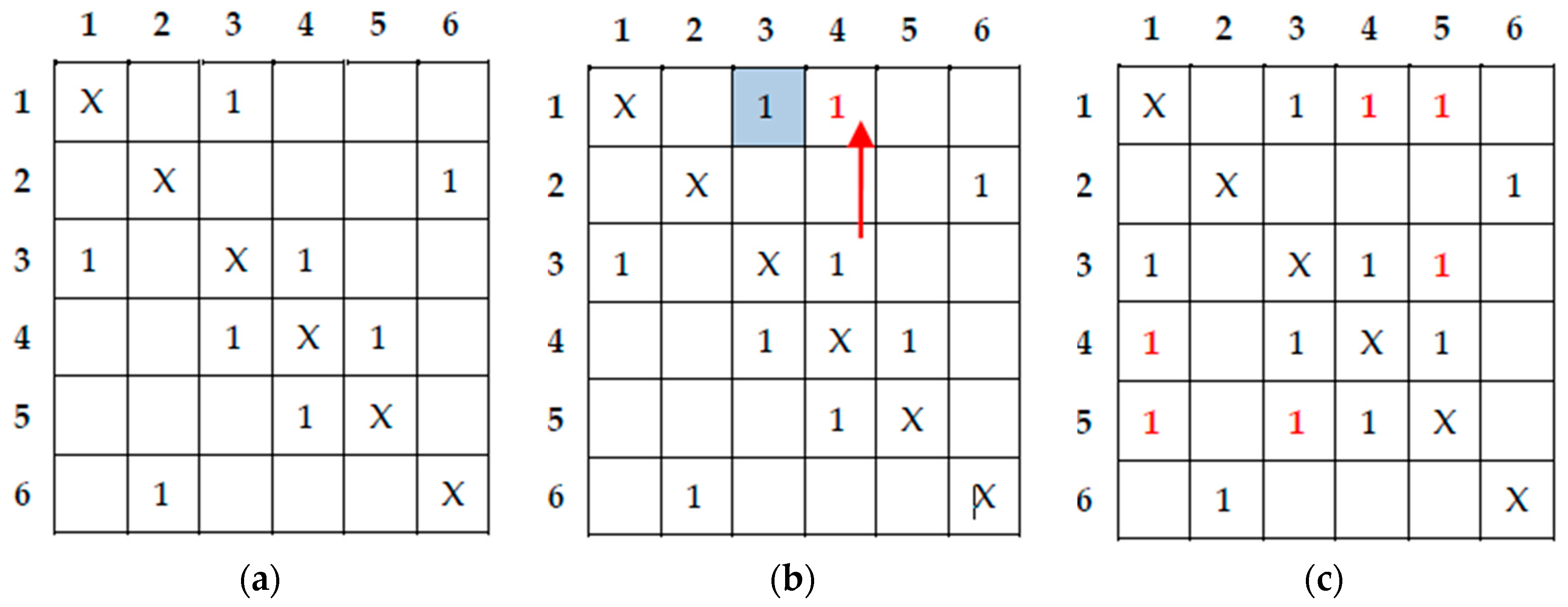
In
Figure 6a, an example of such a 2D table sub-system is reported. We suppose that six labels have been assigned, thus, all elements on the diagonal line were written with a logic of one. Since such elements do not play a role in the subsequent phase, in which collisions are resolved, we filled those positions with ‘X’. Furthermore, several collisions were identified during the provisional labeling step and consequently other positions in the table were filled with a logic of one. The collisions in the example of
Figure 6a are (1-3), (3-4), (2-6), and (4-5); no matter the order in which they were found. It is worth noting that a collision chain is present (1-3, 3-4, 4-5).
When the
Last signal is asserted, the update phase starts. The register file is now scanned row-by-row. In the position (1,3) a logic of one is found and this means that the third row must be copied to the first row, as shown in
Figure 6b. This process is repeated iteratively until the current row is updated. When the update is complete, the table appears as in
Figure 6c. A leading one circuit is used to find the position of the first logic of one in each row, thus obtaining the equivalences that are then stored in the
Label Translator LUT. The completion of the operation is flagged by the signal
Completed visible in
Figure 4. In the above example, labels 1, 3, 4, and 5 are all translated as 1, whereas labels 2 and 6 are translated as label 2. Finally, such information is used by the subsequent processing stages, as above described.
5. Results
The architecture of
Figure 2 has been implemented in the hardware with
NL = 64 by using a Xilinx Zynq-7000 AP-SOC xc7z045ffg900-2 chip to prove its functionality and to measure the speed of performance. To this purpose, the German Traffic Sign Recognition Benchmarks (GTSRB) [
22] have been used. For a fair comparison with competitors, a 640 × 480 image resolution has been adopted, and all the pre-processing segmentation steps have been not included in the following comparison.
The characteristics of the proposed CCL architecture and of several competitors are summarized in
Table 1. It can be easily observed that the proposed architecture significantly overcomes the speed performance of competitors in [
9,
10,
16], well above the improvement expected due to the more advanced technology used here. When implemented within a XC7Z045 chip, the complete embedded system depicted in
Figure 2 uses 51%, 15.5%, and 3.6% of the available LUTs, FFs, and BRAMs, respectively. The maximum achievable clock frequency is 225 MHz, which is well below the maximum frequency sustainable by the AXI4 and AXI4-Stream DMA interfaces. It was obtained by the Vivado Timing Analyzer for the whole system depicted in
Figure 2. Besides the maximum clock frequency, that is obviously dependent on the technology adopted in the various realizations,
Table 1 reports the number of latency cycles and the throughput in terms of number of cycles per pixel that are technological-independent speed performance parameters. Such data were directly extracted from original papers. The particular strategy adopted in the proposed design allows the lowest latency to be reached. Furthermore, the number of clock cycles required to obtain an output pixel is almost halved with respect to [
10,
16] and 18% lower than the architecture in [
9]. All these advantages are obtained at a reasonable expense of the logic resources requirement, and without using internal and/or external memory resources.
With respect to the system demonstrated in [
17], it should be noted that such an implementation uses hardware resources only for the provisional labeling portion of the architecture, whereas the label collisions resolution is executed by a software routine using further external memory resources not included in the table. However, for a direct comparison, we have implemented the provisional labeling circuit described in
Section 4.1 on the Zynq xc7z020clg484-1 chip. Results show that for the provisional labeling portion, only 404 LUTs and 770 FFs are required, saving precious BRAM resources, and achieving a performance of ~140 Mpixels/s. Consequently, our architecture provides an 4.6× improvement in terms of performance/area efficiency over [
17].
Further hardware experiments have been performed to verify if the collisions resolution phase is totally or partially hidden by the DMA
1 configuration process. By using benchmarks in [
22] and the
Internal Logic Analyzer (ILA), we proved that the worst-case time required to prepare the
Label Translator LUT is less than 5 μs, whereas the DMA configuration needs at least 15 μs to be completed. In the test set-up, pre-processed image benchmarks have been stored in the DDR memory by means of an off-line process. Then, an on-purpose C++ routine was executed on the ARM-processor that programmed the DMAs activity and started the CCL computation. Finally, the output labeled image was stored to the DDR memory again for testing purposes. Such results were compared with those obtained through Matlab routines. ILA measurements have been used to verify the correctness of all timing actions.
The theoretical worst-case collisions resolution time has been estimated at ≈29 μs, but it has been verified that it can occur only in the presence of an unrealistic chain of label collisions. However, we artificially forced the 2D table to assume such an unrealistic content. In this case, the
Completed signal in
Figure 4 would delay the start of the DMA
1 transfer by ≈14 μs. As a consequence, the maximum sustainable frame rate would be 717 fps, instead of 724 fps which is reachable when the resolution time is totally overlapped with software code execution.
To measure energy use, the Xilinx Power Analysis Tool was used to execute a real estimation based on the switching activity of the internal signals when the theoretical worst-case image is fed as an input to the architecture. In such a situation, the dynamic energy dissipation is 620 μJ for the Provisional Labeling Circuit and the 2D table. When the proposed system is used to process a 640 × 480 frame at 60 fps, the dynamic power dissipation is 38 mW, which is ≈21% lower than the architecture in [
16], in the same operating conditions.
Finally, the proposed Zynq-based embedded system has been compared with an all software implementation of the same CCL algorithm. A software code running on the ARM dual-core processor was used to evaluate the execution time required for reading a 640 × 480 input image from the DDR3, performing the provisional labeling based on the rules described in
Section 3.1, writing and updating the 2D Table, and storing the result into the external memory. The processor completes those tasks in 8.6 ms, running at 666.66 MHz as the clock frequency. However, the hardware implementation performs the tasks in 1.38 ms, at a clock frequency of 225 MHz, providing an increase is speed of 6.23× with respect to the software counterpart.
6. Conclusions
A novel Connected Component Labeling architecture specifically designed for the inclusion in heterogeneous image-processing embedded systems has been demonstrated. The main innovation consists in overlapping the label collisions resolution phase and the Direct Memory Access cores configuration actions performed by the ARM processors.
Such a strategy allows a throughput rate of ~220 Mpixels/sec to be reached at the reasonable expense of logic resources widely available in the programmable logic of a Xilinx Zynq-7000 AP-SOC. The proposed design saves precious Block-RAM resources and does not use the external memory to accomplish the CCL task, but rather the external memory is used just as a frame buffer. A frame rate higher than 700 fps is obtained when a 640 × 480 image resolution is adopted, while only 620 μJ are used in the worse-case scenario. When the target application requires the elaboration of Full HD images at 60 fps, ~1300 more FFs are utilized and, to save power, the clock frequency can be as low as 125 MHz.


