Ferroelectric Polarization Aided Low Voltage Operation of 3D NAND Flash Memories


1
Department of Electrionics Engineering, Korea National University of Transportation, Room No. 307, IT Building, 50 Daehak-ro, Chungju-si, Chungbuk 27469, Korea
2
Faculty of Electronic and Electrical Engineering, Hankyong National University, Anseong-si 17579, Korea
3
Department of IT and Energy Convergence (BK21 FOUR), Korea National University of Transportation, 50 Daehak-ro, Chungju-si, Chungbuk 27469, Korea
*
Authors to whom correspondence should be addressed.
Electronics 2021, 10(1), 38; https://doi.org/10.3390/electronics10010038
Submission received: 10 December 2020
/
Revised: 23 December 2020
/
Accepted: 26 December 2020
/
Published: 29 December 2020
(This article belongs to the Special Issue New CMOS Devices and Their Applications)
Abstract
:In this paper, we proposed a novel structure enabling the low voltage operation of three-dimensional (3D) NAND flash memory. The proposed structure has a ferroelectric thin film just beneath the control gate, where the inserted ferroelectric material is assumed to have two stable polarization states. A voltage for ferroelectric polarization (VPF) that is lower than the program or erase voltage is used to toggle the polarization state of the ferroelectric thin film, whose impact on the channel potential profile is analyzed to optimize operation voltage reduction. The channel potential of select word line (WL), where the natural local self-boosting (NLSB) effect occurs, increases due to the polarization state. Model parameters for the ferroelectric thin film of 8 nm are fixed to 15 µC/cm2 for remanent polarization (Pr), 30 µC/cm2 for saturation polarization (Ps), and 2 MV/cm for coercive field (Ec). Within our simulation conditions, a program voltage (VPGM) reduction from 18 V to 14 V is obtained.
1. Introduction
The growing demand for data storage devices such as solid-state drives (SSD), mobile phones, and data centers has been supported by high density NAND flash memories. Their classical two-dimensional implementation [1,2] has been revolutionized to current three-dimensional (3D) NAND flash technologies based on cell stacking [3,4,5]. Further development is necessary to mitigate conventional cell-to-cell interference, reliability, and newly investigated issues [6,7,8]; which can be accomplished by operation voltage reduction of memory cells. In this paper, a low voltage NAND flash memory cell is proposed with ferroelectric thin film just beneath the control gate, where ferroelectric polarization gives an auxiliary biasing for the reduction of program or erase voltages. If the ferroelectric thin film is used, program disturb decreases because high channel potential of selected WL reduces the program disturb in the inhibited string. When the channel potential of selected WL is increased, the program disturb is decreased in the inhibited string. Therefore, we analyzed the channel potential of the proposed structure in this paper. In addition, the natural local self-boosting (NLSB) effect of selected word line (WL) in the inhibited string was analyzed according to the voltage for ferroelectric polarization (VPF) [9,10]. The channel potential of proposed structure was compared with the channel potential of conventional structure. The 3D technology computer-aided design (TCAD) simulation was conducted to analyze the characteristic of the proposed structure, in which ferroelectric materials are with the ferroelectric permittivity model in ATLAS SilvacoTM [11,12].
2. Proposed Structure and Operation
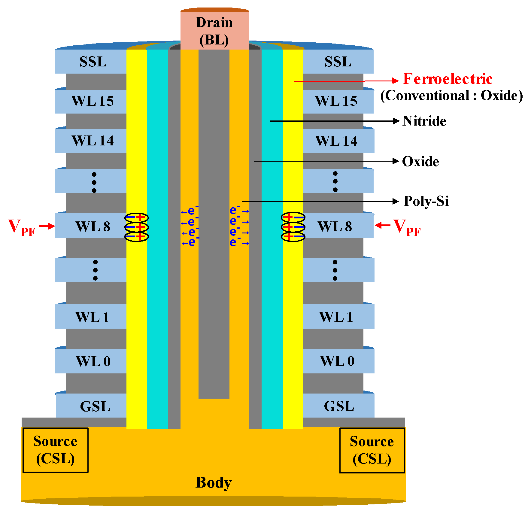
Figure 1 shows the proposed structure, which is composed of 16-word lines, string select line (SSL), ground select line (GSL), bit line (BL), and common source line (CSL). In this structure, the WL 8 was specified as the selected WL. The conventional structure consists of silicon, oxide, nitride, oxide, and silicon (SONOS) [13,14,15], where the ONO thickness combination is 8 nm, 8 nm, 4 nm. The proposed structure has ferroelectric thin film replacing the oxide beneath the control gate. Model parameters for the ferroelectric thin film are set as follows: 15 µC/cm2 for Pr, 30 µC/cm2 for Ps, and 2 MV/cm for Ec. The voltage for the ferroelectric polarization is smaller than the program voltage (or the absolute value of the erase voltage), and its application gives one of two stable polarization states in the ferroelectric thin film. Positive VPF is applied prior to the program operation, when downward polarization is built in the ferroelectric thin film as illustrated in Figure 1. This downward polarization gives an auxiliary positive biasing on the tunnel oxide and nitride dielectric layers, which gives reduction in program voltage that is applied subsequent to the VPF.
Figure 2 shows the timing diagram of the WL 8 in the proposed structure. The VPGM is fixed at 18 V, in addition, variable VPF is applied for optimization. During the program operation, the pass voltage (VPASS) of 6 V is applied to unselected WL. Meanwhile, 2.4 V is applied to SSL and bit line (BL). The channel potential profiles are collected at t1 and t2.
3. Results and Discussions
Figure 3 shows the channel potential profiles when VPF ranged from 3 V to 7 V. The VPF time was fixed to 2 µs because VPF time did not significantly affect the channel potential. As a result, the channel potential reached the maximum value when VPF was 4 V. However, when VPF is increased from 4 V to 7 V, the channel potential of WL 8 also decreased. The most suitable value of VPF in this range is, therefore, 4 V, as the maximum channel potential was obtained.
In Figure 4, the channel potential profiles at VPF of 4 V with a fixed pulse width of 2 µs, where the delay time between VPF and VPGM (T1) is varied from 1 to 4 µs. In Figure 4a, when T1 was 1 µs, the lowest channel potential was obtained. Furthermore, the channel potential increased with T1, as the polarization phenomenon positively affected the channel potential during T1. As a result, with the increase of T1, the duration in which the increased channel potential lasted longer. This conclusion is also supported by the results shown in Figure 4b. The channel potential of WL 8, where the natural local self-boosting effect occurs [10], also increased with T1.
Figure 5a shows the channel potential profiles obtained from the proposed and conventional structures when VPGM was 18 V. The highest values of channel potential of the conventional and proposed structures were 12.12 V, 13.95 V, and 15.64 V, respectively. The channel potential of proposed structure with 3.9 for ferroelectric permittivity (εf) is higher than that of the conventional structure. This result means the polarization phenomenon positively influenced the channel potential of WL 8. In addition, the channel potential of proposed structure with default value (200) of εf is highest since the more polarization occurs if the permittivity is higher. Therefore, the ferroelectric thin film can increase the channel potential because of the high permittivity and the polarization phenomenon.
As a result, in the proposed structure, the same effect as that when 18 V is applied to the conventional structure can be obtained even if VPGM is lowered. When VPGM was 14 V, considering the proposed structure, the channel potential of WL 8 was the same as that of the conventional structure, as shown in Figure 5b. The voltage reduction obtained from these results is a significant advantage of the proposed structure for the 3D NAND flash memory.
When using a ferroelectric thin film, it may be difficult to make a thin film due to a process problem. In addition, since blocking oxide is used as a ferroelectric thin film, leakage current may occur. However, if several drawbacks of ferroelectric material are further studied, they can be sufficiently used in mass production because they have great advantages.
4. Conclusions
In this paper, we proposed a novel structure composed of ferroelectric material for the 3D NAND flash memory. When VPF was applied to the WL 8, the channel electrons of the neighbor cells migrated to the WL 8. The channel potential increased with T1 as the polarization phenomenon improved the channel potential during T1. In addition, experiments with different VPF were conducted to obtain the voltage (4 V) that maximized the channel potential. The maximum channel potential of the proposed structure was higher than that of the conventional structure. Therefore, the same electrical behavior of the conventional structure when VPGM was 18 V can be observed when VPGM was lowered to 14 V with the proposed structure, which is a significant advantage for the 3D NAND flash memory.
Author Contributions
Investigation, Y.J.; Data curation, I.H.; visualization, I.H.; software, I.H.; validation, Y.J.; project administration, M.K.; funding acquisition, M.K.; supervision, M.K.; writing—original draft preparation, I.H.; writing—review and editing, S.J.B. All authors have read and agreed to the published version of the manuscript.
Funding
This research was supported by National R&D Program through the National Research Foundation of Korea (NRF) funded by Ministry of Science and ICT (2020M3F3A2A01085755) and in part by Basic Science Research Program through the National Research Foundation of Korea (NRF) funded by the Ministry of Education (2018R1A6A1A03023788) and in part by the MOTIE (Ministry of Trade, Industry & Energy (10085645) and KSRC (Korea Semiconductor Research Consortium) support program for the development of the future semiconductor device and in part by grants from National Research Foundation (NRF), Republic of Korea (Grant No. NRF-2017R1D1A1B03029764).
Institutional Review Board Statement
Not applicable.
Informed Consent Statement
Not applicable.
Data Availability Statement
Data sharing not applicable. No new data were created or analyzed in this study. Data sharing is not applicable to this article.
Conflicts of Interest
The authors declare no conflict of interest.
References
- Kang, M.; Lee, K.; Chae, D.-H.; Park, B.-G.; Shin, H. The compact modeling of channel potential in sub-30nm NAND flash cell string. IEEE Electron Device Lett. 2012, 33, 321–323. [Google Scholar] [CrossRef]
- Park, Y.; Lee, J.; Cho, S.-S.; Jin, G.; Jung, E. Scaling and reliability of NAND flash devices. In Proceedings of the 2014 IEEE International Reliability Physics Symposium, Waikoloa, HI, USA, 1–5 June 2014. [Google Scholar]
- Kang, M.; Park, I.; Chang, I.; Lee, K.; Seo, S.; Park, B.-G.; Shin, H. An accurate compact model considering direct-channel interference of adjacent cells in sub-30-nm NAND flash technologies. IEEE Electron Device Lett. 2012, 33, 1114–1116. [Google Scholar] [CrossRef]
- Kim, Y.; Kang, M. Predictive modeling of channel potential in 3-D NAND flash memory. IEEE Trans. Electron Devices 2014, 61, 3901–3904. [Google Scholar] [CrossRef]
- Kim, Y.; Yun, J.-G.; Park, S.-H.; Kim, W.; Seo, J.; Kang, M.; Ryoo, K.-C.; Oh, J.-H.; Lee, J.-H.; Shin, H.; et al. Three-dimensional NAND flash architecture design based on a single-crystalline stacked array. IEEE Tran. Electron Devices 2012, 59, 35–45. [Google Scholar] [CrossRef]
- Kang, M.; Hahn, W.; Park, I.-H.; Song, Y.; Lee, H.; Choi, K.; Lim, Y.; Joe, S.-M.; Chae, D.-H.; Shin, H. A compact model for channel coupling in sub-30 nm NAND flash memory device. Jpn. J. Appl. Phys. 2011, 50, 100204. [Google Scholar] [CrossRef]
- Lee, G.; Kim, Y.; Jeon, J.; Kang, M. Analysis of NLSB effect depending on cell pattern and bias conditions in 3D NAND flash memory. In Proceedings of the International Conference on Electronics, Information, and Communication, Honolulu, HI, USA, 24–27 January 2018; pp. 962–963. [Google Scholar]
- Jeong, Y.; Lee, G.; Jeon, J.; Jhon, H.-S.; Kim, Y.; Kang, M. Analysis of natural local self-boosting effect due to down-coupling phenomenon in 3D NAND Flash Memory. In Proceedings of the International Conference on Solid State Devices and Material, Tokyo, Japan, 9–13 September 2018; pp. 921–922. [Google Scholar]
- Kim, Y.; Kang, M. Down-coupling phenomenon of floating channel in 3D NAND flash memory. IEEE Electron Device Lett. 2016, 37, 1566–1569. [Google Scholar] [CrossRef]
- Kang, M.; Kim, Y. Natural local self-boosting effect in 3D NAND flash memory. IEEE Electron Device Lett. 2017, 38, 1236–1239. [Google Scholar] [CrossRef]
- Jeong, Y.; Baik, S.-J.; Kang, M. Study of program scheme using ferroelectric material in 3D NAND flash memory. In Proceedings of the International Conference on Electronics, Information, and Communication, Barcelona, Spain, 19–22 January 2020; pp. 360–362. [Google Scholar]
- Atlas User’s Manual, Silvaco Version. 5.19.20. Available online: http://www.silvaco.com/products/tcad/device_simulation/atlas/atlas.html2019 (accessed on 1 January 2019).
- Jeong, Y.; Ham, I.; Kang, M. Optimal bias condition of dummy WL for sub-block erase operation in 3D NAND flash memory. In Proceedings of the International Conference on Solid State Devices and Material, Aichi, Japan, 2–5 September 2019; pp. 683–684. [Google Scholar]
- Seo, Y.; An, H.-M.; Song, M.-Y.; Kim, T.-G. Charge trap flash memory using ferroelectric materials as a blocking layer. Appl. Phys. Lett. 2012, 100, 173507. [Google Scholar] [CrossRef]
- Jeong, Y.; Ham, I.; Han, S.; Kang, M. Optimal dummy word line condition to suppress hot carrier injection phenomenon due to the natural local self-boosting effect in 3D NAND flash memory. Jpn. J. Appl. Phys. 2020, 59, 1–5. [Google Scholar] [CrossRef]
Figure 1.
Proposed structure with ferroelectric thin film on top of the nitride.

Figure 2.
Timing diagram of the proposed structure. Pulse duration of VPF, and the delay between VPF and VPGM is indicated as T1.
Figure 2.
Timing diagram of the proposed structure. Pulse duration of VPF, and the delay between VPF and VPGM is indicated as T1.

Figure 3.
Comparison of the channel potential according to VPF at t2 in Figure 2.
Figure 3.
Comparison of the channel potential according to VPF at t2 in Figure 2.

Figure 4.
Channel potential profiles with various T1 periods collected (a) at t1 and (b) at t2.

Figure 5.
Comparison of the proposed structure and the conventional structure. (a) VPGM was 18 V for structures; (b) VPGM was 14 V for the proposed structure.
Figure 5.
Comparison of the proposed structure and the conventional structure. (a) VPGM was 18 V for structures; (b) VPGM was 14 V for the proposed structure.

Publisher’s Note: MDPI stays neutral with regard to jurisdictional claims in published maps and institutional affiliations. |
© 2020 by the authors. Licensee MDPI, Basel, Switzerland. This article is an open access article distributed under the terms and conditions of the Creative Commons Attribution (CC BY) license (http://creativecommons.org/licenses/by/4.0/).
Share and Cite
MDPI and ACS Style
Ham, I.; Jeong, Y.; Baik, S.J.; Kang, M. Ferroelectric Polarization Aided Low Voltage Operation of 3D NAND Flash Memories. Electronics 2021, 10, 38. https://doi.org/10.3390/electronics10010038
AMA Style
Ham I, Jeong Y, Baik SJ, Kang M. Ferroelectric Polarization Aided Low Voltage Operation of 3D NAND Flash Memories. Electronics. 2021; 10(1):38. https://doi.org/10.3390/electronics10010038
Chicago/Turabian StyleHam, Ilsik, Youngseok Jeong, Seung Jae Baik, and Myounggon Kang. 2021. "Ferroelectric Polarization Aided Low Voltage Operation of 3D NAND Flash Memories" Electronics 10, no. 1: 38. https://doi.org/10.3390/electronics10010038
Note that from the first issue of 2016, this journal uses article numbers instead of page numbers. See further details here.