
Practical Challenges of High-Power IGBT’s I-V Curve Measurement and Its Importance in Reliability Analysis


1
IMO-IMOMEC, Hasselt University, Wetenschapspark 1, 3590 Diepenbeek, Belgium
2
Imec, Kapeldreef 75, 3001 Heverlee, Belgium
3
EnergyVille, Thor Park 8310, 3600 Genk, Belgium
*
Author to whom correspondence should be addressed.
Electronics 2021, 10(17), 2095; https://doi.org/10.3390/electronics10172095
Submission received: 7 July 2021
/
Revised: 18 August 2021
/
Accepted: 26 August 2021
/
Published: 29 August 2021
(This article belongs to the Special Issue Recent Developments and Emerging Trends in Power Electronics Converters)
Abstract
:This paper examines the practical challenges of simplified setups aimed at achieving high-power IGBTs’ IC–VCE curve. The slope of this I–V curve (which is defined as on-resistance RCE) and the point where the VCE–VGE curve visibly bends (threshold gate voltage) can be suitable failure precursor parameters to determine an IGBT’s health condition. A simplified/affordable design for these specific measurements can be used for in-situ condition monitoring or field testing of switching devices. First, the possible I–V curve measurement methods are discussed in detail in order to prevent self-heating. The selected design includes two IGBTs in which the high-side IGBT was the device under test (DUT) with a constant gate voltage (VGE) of 15 V. Then, the low-side IGBT was switched by a short pulse (50 μs) to impose a high-current pulse on the DUT. The VCE–VGE curve was also extracted as an important failure-precursor indicator. In the next stage, a power-cycling test was performed, and the impact of degradation on the IGBT was analyzed by these measurement methods. The results show that after 18,000 thermal cycles, a visible shift in I–V curve can be seen. The internal resistance increased by 13%, while the initial collector-emitter voltage and voltage at the knee point in the VCE–VGE curve slightly changed. It is likely that in our case, during the performed power-cycling test and aging process, the bond wires were most affected, but this hypothesis needs further investigation.
1. Introduction
Today, power semiconductor devices have become an integral part of power electronic circuits, and advances in these devices have had a huge impact on related industries as high-power circuit designs have become possible. Since bipolar power transistors offer a low-current gain, placing these bipolar transistors in high-voltage fields will significantly increase the size and weight of the designed circuit; by its nature, the cost of the system will be also escalated [1]. As an insulated-gate bipolar transistor (IGBT) is a combination of metal–oxide semiconductor field-effect transistor (MOSFET) and bipolar junction transistor (BJT), it has inherited the positive features of both the transistor and MOSFET [2]. For this reason, while designing a high-power circuit, much attention is paid to the correct choice of the IGBTs in accordance with the relevant application. Nevertheless, the designers should consider the practical limitations of the power semiconductor device and have a good understanding of all the operating details of the selected IGBT. Perhaps the most important characteristic that the designer should pay attention to is the electrical characteristics of the IGBT. Different performance characteristics curves are provided in the datasheet by the manufacturer, and with a closer look at them, it can be predicted that the selected IGBT is suitable for the desired application. Among these different curves, the IC–VCE curve is enormously important, as it shows the relationships between the collector current (IC) and the collector-emitter voltage (VCE) at different gate-emitter voltages (VGE) and different temperatures (Tj) [3]. To properly exploit the electrical characteristics, it is essential that the IGBT’s I–V curve be evaluated over the entire device operation range. Additionally, extraction of this diagram is critical because this curve is mainly needed to estimate the conduction power losses [4].
Since the IGBTs under study usually have a high-rated current, there are some practical challenges to measure these high-power I–V curves. To obtain the I–V curve for higher range of current, a power device analyzer/curve tracer can be used to read the collector-emitter voltage (VCE) at a constant gate voltage while applying a short, high-current pulse. Then, the amplitude of this current pulse is increased in sequence, and the full-range I–V curve is obtained point by point. The main problem with power-curve tracer devices is that they are very expensive and not available to all laboratories. Secondly, most laboratories use early models of this device, such as Tektronix 370B or Scientific Test 5000C, which have a maximum current limit of 20 A and 50 A, respectively. Another issue that can happen during the measurements is self-heating if the period of these high-current pulses gives the IGBT a chance to heat up. In early power-curve tracers, the current pulse is usually about 300 μs, which can possibly be enough time for self-heating, making the measurement inaccurate [5]. It should be noted that there are some new devices with 10 μs pulse-width measurement capability and currents up to 1500 A (i.e., Keysight B1505A), but the main deterrent in using this equipment is its price.
Although various studies have employed commercial power device analyzers/curve tracers to extract IGBT’s I–V curve (e.g., [6,7]), there are a few prior studies on this subject and the possibilities for measuring high-power I–V curves; most of these studies examined a MOSFET as the device under test (DUT) [8,9,10,11,12]. These studies have not fully discussed the implementation steps of their test setup, so the re-implementation of these setups is practically impossible, and the technician would facing various challenges during the design process. For instance, Basler et al. [5] investigated a combined approach based on the short-circuit and curve-tracing techniques in order to measure a complete I–V curve for a high-power IGBT up to its breakdown point. The design details on how to measure the complete I–V curve were not given in this study. A double-pulse test circuit was presented in [13,14,15], using a double-pulse signal applied to the gate of the IGBT, switching the IGBT two times. During the first pulse, a current was stored into an inductive load, and the voltage and current waveforms were measured by the oscilloscope when the first pulse as turned off, and the second pulse was applied to the gate. Unfortunately, the details of the implementation process of this test were not provided. As the commercial I–V curve-tracer devices are relatively expensive, Choi et al. [16] proposed a bridge circuit including four pairs of IGBTs/diodes so as to obtain the I–V curve of the DUT. Although the introduced method seems interesting, the details of the implementation of this measurement method were not provided, which makes it difficult to re-implement this system; for example, the switching sequences are not specified. A simplified method with two series IGBTs to extract I–V curves was proposed by Chen et al. [17]. There are no provided details of the circuit-implementation process. For example, this paper states that the current pulse amplitude is set to certain values by a current source. But in practice, by switching one of the IGBTs, the current source will be switched, which always includes a delay, and it will not be possible to produce short, high-current pulses. Du et al. [18] established a simple test setup including a high-power Keithley 2651A source meter unit (SMU) and a low-current Keithley 2636B SMU. In this setup, one of the SMUs is connected directly to the two ends of the collector and the emitter, and the other SMU is utilized to supply an accurate gate voltage. Although the measurement accuracy in this case is remarkable, the minimum pulse width that can be defined for this power supply (Keithley 2651A) is 100 μs, which is strongly dependent on the resistance of the device under test. For example, as the rise time for the generated pulsed current is strongly subjected to the load resistance, the production of short current pulses is limited for MOSFETs with higher on-state resistances.
As can be found from the literature, a common gap among these studies is that the detailed process of implementing the measurement circuit is not provided, which makes it difficult or impossible for the reader to re-implement these circuits. In addition, there is no comparison between short and long current pulse measurements to show the real influence of current pulse duration on the measurement accuracy.
IGBTs are always exposed to severe operating conditions, which lead to different types of intrinsic and extrinsic failures; consequently, understanding the physics of failures has become essential in this regard [19]. Thus, condition monitoring of IGBTs to identify potential packaging-related failure mechanisms (e.g., die-attach fatigue and bond wire lift-off) can have a significant impact on system-level reliability. In prior studies, several indicators have been selected to be monitored during the operation of IGBTs, and the change in each of these indicators indicates a specific type of failure. For example, the on-state collector-emitter voltage (VCE(on)) was used in [20] to show the solder-fatigue mechanism. Another meaningful parameter of the IGBT whose change indicates the degradation of the die-attach layer and bond wire lift-off is the on-resistance (RCE(on)), which has received less attention [21,22]. The on-state collector-emitter resistance is measured as reciprocal of the slope of the linear curve of IC–VCE graph. Although this resistance may be measured directly by a multimeter by floating the collector as described in [23], it is important to have a complete I–V curve, as it is the main characteristic of the IGBT under test [24]. Moreover, combining this parameter with the threshold gate voltage can provide valuable information about an IGBT’s state of health.
Since the issue of a power semiconductor device’s reliability is considered very important for today’s industries [25], it is not without merit to consider and investigate the correlation between the aforesaid measurements and reliability assessment of power devices. There are different reliability indicators for power semiconductor devices, such as threshold gate voltage (VGE_th), collector-emitter voltage (VCE), thermal resistance (Rth), and on-state resistance (RCE) [22,26,27]. Each of these indicators can indicate a specific type of failure within the IGBT package. To accelerate the aging process within the IGBTs, a power-cycling test is performed as a high-current pulse is applied to the collector of the IGBT to raise the junction temperature; then, the current is cut off so that the IGBT has a chance to cool down. This thermal cycle is repeated many times and over time, causes thermal stress in the different material layers of the IGBT [28]. During the power-cycling test, there is always an increase in voltage VCE, which is mainly due to the degradation of the materials used in bond wires and metallization [29]. At the end of the power-cycling test, a sharp rise in voltage VCE can possibly be seen, which also increases the thermal resistance Rth. This sharp spike in the measured voltage can be attributed to possible cracks in the solder layer between the silicon chip and the copper substrate [26]. Mainly, if the change in collector-emitter voltage (VCE) or thermal resistance (Rth) exceeds a certain limit (e.g., 5–20% [30]), it indicates a failure/fracture in the IGBT. According to [31], a slight change in the initial collector-emitter voltage was observed due to the solder lead degradation by comparing a new IGBT with an aged IGBT. The threshold gate voltage (VGE_th) may also vary during the degradation process, which can disrupt normal switching characteristics and reduce the operating frequency [32]. Deviation in the voltage VGE_th is mostly due to gate-oxide defects [33].
Liu et al. [34] examined the effect of degradation on the IGBT’s I-V characteristic curve and transient thermal impedance. A shift of I–V curve and an increase in internal resistance could be seen, but the employed method to extract the I–V curve is not clear in this study. Luo et al. [35] modelled the characteristics of an IGBT based on instantaneous on-state resistance (RCE(ON)). In this model, the on-state resistance is a function of the junction temperature (Tj) and collector current (IC). They showed that the RCE(ON) resistance increases by raising the temperature, but the section related to the relation of this resistor to bond-wire failure is incomplete and cursory. A similar study is provided in [36]. The authors used correlation between VCE and Tj to estimate the instantaneous temperature of the IGBT. Meanwhile, after validation of their simulation by several experimental tests, they investigated the effect of cutting bond wires on the VCE voltage. They found that fracture/cracks in the bond wires would increase this voltage. Jia et al. [31] investigated the impact of solder layer degradation on the VCE voltage. They claimed that the solder degradation will cause an increase in operating temperature, which can change the electrical (VCE) and thermal (junction-to-case thermal resistance Rth(j-c)) characterizations of the IGBT over time. Although in this study the effect of solder layer destruction is separated from the bond wires defects, other failure-precursor parameters (e.g., gate threshold voltage and on-state resistance) were not examined.
The research gap that can be highlighted here is that the different reliability indicators are not placed next to each other in order to reach a better conclusion about the failure/fatigue of the IGBTs. Although less attention has been paid to the gate-emitter voltage versus collector-emitter voltage curve (VGE–VCE), this curve can provide a thorough knowledge on the failure modes and mechanisms. By placing this curve next to the IC–VCE curve, the various causes of failure can be possibly monitored.
To override the aforementioned problems, the major purpose of this paper is to find alternative solutions to power-curve tracers and to address practical challenges in high-power IGBT’s I–V curve measurements. The explored simplified/affordable designs will be discussed in this paper, and benefits/drawbacks of each design will be stated in simple language. A main goal of this research is to provide a way to reconstruct this test setup by providing all the design details step by step. As the existing commercial power tracers are considerably expensive and bulky, it may not be very reasonable to use this type of equipment to check for in-situ diagnostic/prognostic condition monitoring or during the power-cycling test of IGBTs. Since the proposed I–V curve-measurement method here is simple and easy-to-implement, it can be easily used in the field to extract the IGBT’s characteristics and obtain a more detailed mission profile for reliability analysis of long-term field tests. This methodology can improve mission-profile-based lifetime-prediction models [37]. The importance of the IGBT’s I–V curve in reliability analysis needs to be further investigated, especially when this curve is placed next to another curve (VGE–VCE) so that the main reason of failure can be better predicted. In this study, the effectiveness of these measurements will be assessed over IGBTs degraded by a power-cycling test as a prove of concept. Besides the I–V curve, the applicability of the gate-emitter voltage versus collector-emitter voltage curve (VGE–VCE) is examined to show the impact of degradation on the IGBT performance. In parallel, this method can be used in field testing and to give feedback to lifetime-estimation models and/or enable predictive condition monitoring of power electronics.
The remainder of this paper is organized as follows. In Section 2, three different possible designs to extract the IGBT’s I–V curve are presented. The test setup for power-cycling test and a proposed integrated circuit are also highlighted in this section. In Section 3, the test results (both long and short current pulses) are provided on the examined IGBT. Comparison of test results on healthy and damaged IGBTs is also presented in this section. Conclusions are drawn in Section 4.
2. Methodology
In this paper, three designs for measuring high-power IGBTs’ I–V curves are presented. In the first case (Figure 1), the IGBT can be directly switched via a gate pulse. This schematic is very simple and easy-to-implement, but the rate of current rise during the turn-on process is limited due to the gate resistor; oscillations excited in intrinsic parasitic elements will make it difficult to control the amplitude of the input current pulse [38].
The problem of oscillations becomes more apparent with increasing the amplitude of high-current pulses. It should be noted that in all the further cases, the power supply can only operate in constant voltage mode (CV). When the power supply is set to a constant current mode (CC) operation, the output flowing current would be zero, as the switch is turned off, and there is no path to the ground. When the IGBT is turned on, the current can flow from the positive of the power source to the negative. This means that while switching the IGBT, in fact, the power source in CC mode is also switching on and off. This will not be desirable for pulses with a shorter time period, as the rise time of the source is around 25 ms for most of the power supplies. By placing a resistor parallel to the switch, the current source can be kept turned on, which in turn raises new challenges. Therefore, the only way that a power supply can be used to perform this experiment is to put the power supply in CV mode. Putting the power supply in its CV mode will bring other challenges. When a power supply is used in CV mode, a resistor must be placed in the circuit path in series with the IGBT. This resistor cannot be large because it must withstand the passage of high-current pulses (high-power rating and resistance <0.1 Ω). Using current sense resistors is one of the easiest solutions to solve this issue. The size of this resistor should be determined according to the amount of current flowing through it so that the voltage drop across the resistor can be measured accurately by an oscilloscope.
The solution to improve the accuracy and eliminate these fluctuations is to keep the switch always turned on by a constant gate voltage, and on the other hand, the current pulse can be applied on the device under test by the fast switching of another power-switching device connected in series. There are two possible circuits based on the aforesaid method as shown in Figure 2: (1) the device under test is placed at the low side, and (2) the device under test is place at the top of another switch (high side).
The priority here is to design the circuit as simple as possible and to perform this measurement technique with minimal laboratory equipment. When the IGBT under test is placed at the low side, the gate voltage of the IGBT can directly be supplied from a voltage source, but the auxiliary switch must be controlled by an isolated/floating voltage pulse. This means that a floating DC source is needed to supply the driver gate, which in turn can complicate the system. Figure 2 represents the way how to connect the floated ground with the respective points in the circuit. Therefore, it is recommended that the IGBT under test is placed at the high side, and the auxiliary switch can be switched directly by a simple low-side gate driver or a high-current pulse generator (e.g., IXDI630CI-ND). In this case, the gate voltage of the DUT is supplied by an isolated DC/DC converter chip (CUI Inc. PQS075-S), which can offer an isolation level of 1.5 kV. The output voltage provided by this converter is internally regulated so that it always keeps the output voltage for supplying the gate constant at 15 volts. Here, an auxiliary switch similar to the test IGBT switch is selected (the typical switching frequency for the chosen IGBT ranges from 20 kHz to 30 kHz, which can provide the required pulse width ~50 μs). The frequency of the signal generator is set to 1 Hz (1 s for each cycle); thus, a short current pulse 50 μs can be generated every one second during the cycle. A MOSFET can also be used as the auxiliary switch, but the problem with MOSFETs is that the internal resistance of the MOSFET (Rds(on) on-state resistance) is usually greater than the current sensing resistor value, and the changes in this MOSFET’s internal resistance are very sensitive to current. Since the voltage of the power supply is limited within a range, the higher currents can be achieved from the power supply at a lower voltage if the total resistance of the circuit is lower, which makes it more reasonable to use IGBTs as the axillary switch instead of MOSFETs. Notably, the problem of altering the resistance value still remains unsolved, and after passing a high-amplitude current pulse, the current sensing resistance value may also change. For this reason, an accurate/fast six-digit multimeter must always be used to measure resistance. In this case, a four-terminal sensing (4T) technique should be employed so that the resistance of the wires is neglected by the multimeter. In the case in which there is a high-frequency current probe available within the required range, this problem is solved on its own.
The next challenge is how to measure the voltage drop across the resistor and the collector-emitter voltage (VCE) of the IGBT under test with an oscilloscope. As oscilloscopes typically are grounded, the voltage difference must always be measured relative to the ground reference. This means that the voltage across the current sensing resistor cannot be measured directly by the oscilloscope. There is a similar problem in measuring the voltage across the IGBT because only the voltage at collector can be measured relative to ground—not the emitter—by the oscilloscope. Here, the method based on the built-in math function is used so that three channels of the oscilloscope are occupied to measure the voltage of three points. Then, the voltage across the resistor is obtained by mathematically subtracting the voltage waveform of CH1 and CH2. The voltage across the IGBT switch is similarly determined by subtracting the CH2 and CH3 voltages. A small voltage/div should be selected for each channel, and the oscilloscope trigger mode should be set to average mode so that the math function output waveform becomes noise free after a few cycles. As the duty cycle for the generated current pulse is very low (D = 50 μs/1 s = 0.005%), measuring voltage and current waveforms after a few cycles is expected to have little effect on the measurement accuracy. The external trigger given by the signal generator can be used to trigger the oscilloscope. This measurement problem can also be easily solved by using a reliable differential voltage probe.
All the inputs (i.e., current sense resistance value and oscilloscope measurements) and the outputs (i.e., gate voltage and high-current pulse width/amplitude) are managed and controlled via a user-friendly LabView interface. The time delay between applied high-current pulses can be altered through the interface and is set to 1 s as a default value.
The next step is to establish the power-cycling test setup as depicted in Figure 3. This simple setup will enable us to force a high current on a discrete IGBT. The IGBT’s saturation voltage (VCESat) at low current (100 mA) would be considered as an indicator for estimating the junction temperature (Tj) of the IGBT. The way to extract the linear relationship between VCESat and Tj is provided in [39]. The voltages and temperatures can be recorded in-situ via a LabView interface during the power cycling for the IGBT under test.
The implemented setup in our case is shown in Figure 4a. This setup enabled us to apply the power cycles on four discrete IGBTs at the same time. The current pulse is controlled directly by the current source: a 30-A pulse as high value and 100 mA as low value. This low current is necessary so that the temperature can be measured from VCE–Tj curve during the cooling phase. The gate voltages for these fours IGBTs under test can be supplied from a reliable floating DC-DC converter. Here, four isolated DC/DC converters were used to supply the gate voltages. The case temperature can be measured by a thermal camera, while the heatsink temperature at different points can be monitored by several thermocouples mounted on the heatsink. Tj can be estimated by reading VCE across each IGBT; thus, it is important to first perform a calibration to find the linear relationship between VCE and Tj for the IGBTs. The VCE values are measured by a 16-channel, 24-bit analog input module. All measurements made during the power cycling test are controlled and displayed by a LabView interface.
The disadvantage of this structure is that to measure the I–V curve, the IGBTs must be taken out of the setup and tested separately. The proposed structure in Figure 4b can solve this problem, as it describes a mixture of the power-cycling test and I–V curve-measurement circuit. A single-pole double-throw relay (SPDT) can take the axillary low side IGBT of the circuit or into the circuit. This auxiliary IGBT can be switched on and off by a short pulse (50 μs) to apply the desired current pulse on the upper switches. In this structure, the collector-emitter voltages should be monitored by an oscilloscope with differential channels (e.g., PicoScope 4444 differential input oscilloscope).
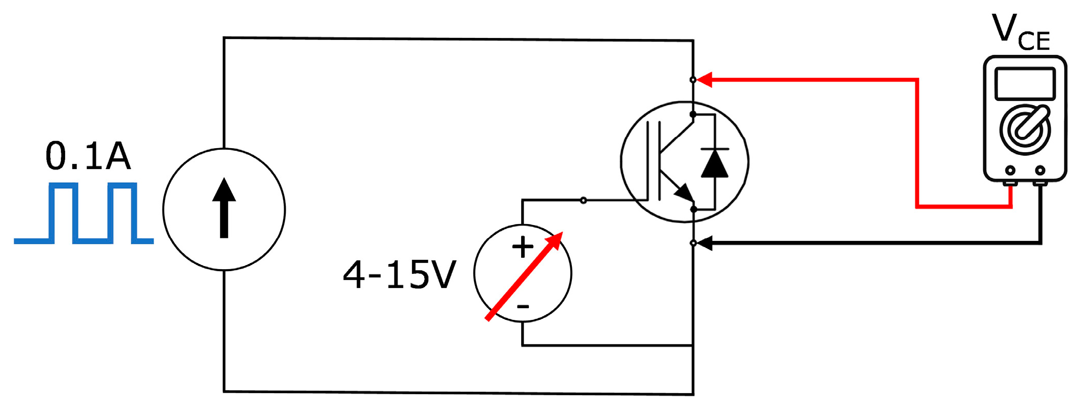
Another measurement that can be done on the IGBTs is to extract the VCE–VGE curve. The knee points at VCE–VGE curve (threshold gate voltage/collector-emitter ON voltage) can also be a suitable failure-precursor parameter to show the IGBT’s health condition (e.g., latch-up) [40,41,42]. When the gate voltage exceeds its threshold, the IGBT acts as an open gate, but it is still not completely turned on until a bias voltage is applied across the collector and emitter. This bias voltage (which is also known as collector-emitter ON voltage) ensures that the carriers reach the emitter from the collector [43]. Operation at high temperature and high electric field is the main reason for the change in the P-N junction and consequently the gate threshold voltage [41]. Here, a simple technique is proposed (Figure 5) that can show the effect of both gate threshold and ON threshold voltages. In this case, a current pulse can be applied across the collector-emitter ends. The amplitude of this current pulse is 100 mA in order to prevent self-heating. VGE can be controlled directly by the power supply; VCE can be monitored by an oscilloscope.
3. Results and Discussion
To validate the obtained experimental results, the IC–VCE curve measured by the manufacturer was extracted from the datasheet. The discrete IGBT under test (700V/40A—ON Semiconductor FGH40T70SHD) is widely used in SMA PV inverters. The full setup is shown in Figure 6. As described in the previous section, to generate the short gate voltages for the low-side IGBT, a low-side gate driver was selected. The input of this gate driver is triggered by an Agilent/Keysight 81101A Pulse Generator after applying rectangular pulse waves (−5 V/+5 V). The duration of the pulse is 50 μs, and the chosen frequency is 1 Hz. To measure the voltage waveforms, a digital oscilloscope (Rigol DS1054Z) was used. Although the typical resolution for this oscilloscope is 8 bits, the oscilloscope’s acquisition mode was set to averaging mode so that it could provide a maximum resolution of 12 bits after a few triggers.
First, the power supply was set to CC mode and was switched itself directly with a 40-ms command signal via a LabView interface. In this case, the IGBT was turned on with a constant gate voltage; then, the current pulses could be generated directly from the power source.
Having the current sensing resistors seemed not to be necessary in this test, as the amplitude of the milli-seconds current pulses could be easily set by the power supply. Since the time interval of these generated current pulses is longer than the self-heating time constant, it was expected that there would be a slight difference in the measurements. An example of this measurement approach is shown in Figure 7. As the command delay was higher than expected, to create a long pulse-measuring case, the power source was switched by a 30-ms long pulse to the gate of the low-side IGBT. To generate the longer current pulses (e.g., >50 ms), the programmable power supply (B&K Precision 9115) can easily supply the desired current determined through the dedicated LabView interface.
It is clear from Figure 8 that the obtained voltage waveforms from the first test setup (Figure 1) showed very high turn-off transients, but the waveforms during the turn-on period showed good results for the desired measuring setpoint. However, achieving a high rate-of-rise of the current was the main obstacle to this test and required better control over the gate driver (e.g., an active control approach should be utilized for the gate control).
To overcome the aforesaid issue, the second test setup (Figure 2b) was employed so that the DUT was always turned on with a constant gate voltage, and an auxiliary switch was used to generate the high-current pulse across the device under test. A drawback of this method is that it is difficult for the oscilloscope to measure the collector-emitter voltage of the top IGBT as well as the voltage drop across the resistor (which represents the current). For this reason, one alternative is to use an oscilloscope mathematical function instead of a high-bandwidth differential probe, so in this case, two mathematical/subtraction functions are needed: (1) to find the voltage of the resistor and (2) to find the voltage of the device under test. An example of this method is shown in Figure 9. As a validation, at a current of 30 A, the obtained VCE over the DUT is 1.56 V, which is in line with the datasheet (~1.53 V @ 30 A).
If a long current pulse (e.g., 30 ms) is applied to the IGBT, in the middle of this pulse when the output from power supply is stabilized, the VCE voltage is close to the values shown in the datasheet. But, in this case, the measurement for the next point should be done after cooling down Tj to 25 °C. It means that if the time delay between the measurements is long enough, and the self-heating effect of the previous test has disappeared, relatively acceptable results can be obtained even with longer pulses. But this measurement technique can take hours to be completed. If the adequate time interval between measurements with a long pulse width is not followed, the results will be a long way from the datasheet. For example, there was 24% difference between the IC–VCE curve in the datasheet and a performed similar test (current pulses 30 ms and a time interval of 5 s between each step).
Two important elements can be extracted from the IC–VCE curve: (1) on-resistance RCE, which is the inverse of the slope of the voltage-current curve and (2) initial collector-emitter voltage VCE0, which is obtained by continuing the linear interval of the curve and the intersection of this line with the horizontal axis. More information is given in [44]. RCE and VCE0 were extracted from the datasheet and the two performed tests (short pulse duration 50 μs and long pulse duration 30 ms). The resistance measured by short pulses was 17.76 mΩ, while the slope of the I–V curve in the datasheet shows a resistance of 13.38 mΩ at a case temperature of 25 °C. The long pulse measurements exhibited a RCE equal to 26.82 mΩ, which highlights the importance of applying short pulses to prevent self-heating. The initial VCE0 extracted from the datasheet is 1.10 V, while for short pulse and long pulse tests, this value was 1.03 V and 0.89 V, respectively.
The next step was to check if there is a difference between a healthy/new IGBT and a defective IGBT in terms of IC–VCE curve and VGE–VCE curve. A high current (30 A) was applied on the IGBTs for 5 s; the IGBTs were then rested for 7 s without applying current while being cooled rapidly by the cooling system. After applying 18,400 high-∆Tj cycles (95 °C) to the IGBTs, one of these components excessed the allowable variation, as shown in Figure 10.
As described in the previous section, the I–V curve was extracted for a healthy IGBT and an aged IGBT after 18,000 thermal cycles, shown in Figure 11.
The curve extracted from the datasheet is also shown in Figure 11. By increasing current, the distance between the measure curve and the graph obtained from the datasheet increased, so that at a current of 40 A, a difference of 3.7% was observed. The important point to note here is that the shortest path to the IGBT legs should be selected for oscilloscope measurement. This is because the connections themselves have a resistance that changes during the passage of a high-current pulse, causing a measurement error. This difference can be also further reduced by longer interruptions between the measurements.
A shift is clearly visible in the measured I–V curve. As is clear from Figure 11, by increasing the amplitude of the pulse current, these two graphs become more distant from each other. Additionally, the collector-emitter resistance (RCE) and initial collector-emitter voltage (VCE0) derived for the aged IGBT are 20.01 mΩ and 1.007 V, respectively. Therefore, it was confirmed that the resistance increased by about 13% during the degradation process (RCE_Healthy = 17.76 mΩ). According to [44], although this resistance (RCE) is the sum of the resistances of the chip, bond wires, and terminal connections, only the resistance of the bond wires changed considerably during the degradation and aging process. The initial voltage (VCE0) was reduced to 1.00 V from the previous value of 1.03 V, which only showed a slight change.
The second curve (VGE–VCE) was extracted as depicted in Figure 12. In this case, the gate voltage was varied in a range of 4 V to 15 V with a step of 0.05 volts, while the collector current was fixed at 100 mA. It can be seen that the knee point in this diagram dropped by 0.2 V to 6.0 V. Additionally, the saturated voltage at 100 mA was reduced from 0.71 V to 0.68 V. The gate-to-emitter threshold voltage (the knee point at the top left) is defined as the minimum bias voltage required to flow current through the collector-emitter. In this experiment, this voltage increased by about 3% (from 5.40 V to 5.55 V). Putting this curve and the previous I–V curve together, it can be concluded that the major degradation was related to the bond wires (as the on-state resistance changed significantly), and the degradation had only a small effect on the inversion layer and gate oxide.
4. Conclusions
In this paper, various possibilities for extracting high-power IGBTs’ IC–VCE curve are presented. Disadvantages, advantages, and challenges of each case are described in detail. According to the experiments, the best circuit for measuring the I–V curve is the one with an auxiliary switch at the low side that is switched by a pulse generator and a low-side gate driver; additionally, the IGBT under test is placed at the high side, and it is always turned on by a constant gate voltage. The curve extracted from the datasheet was used as a reference for validation. The measurements made by the proposed setup were able to provide acceptable results. In the next step, a power-cycling test was done through a dedicated setup with four discrete IGBTs. The conventional power-cycling circuit was modified by adding an auxiliary switch and a SPDT relay so that the power-cycling test and the I–V measurements could be performed at the same setup.
Comparison of the curves of a healthy IGBT and an aged IGBT shows that the electrical resistance (RCE) of the degraded IGBT increased by about 13% during the degradation process, while the initial collector-emitter voltage (VCE0) did not show much sensitivity. The VGE–VCE curve is also provided to show the influence of IGBT operation at high temperatures or high electric fields. The values at the two knee points were compared, and it was found that this aging process did not have a significant effect on the gate threshold voltage. It is likely that in our case, the bond wires are most affected during the performed power-cycling test and aging process. A more detailed study, including images from scanning electron microscope (SEM) and scanning acoustic microscope (SAM), can be considered as the next step. Performing these tests on a greater number of samples alongside X-ray and scanning acoustic microscopy images can be considered as a future study. In parallel, this method can be used in field testing and give feedback to lifetime estimation models and/or enable predictive condition monitoring of power electronics.
Author Contributions
Conceptualization, O.A. and M.D.; methodology, O.A.; software, O.A. and L.V.C.; validation, O.A.; formal analysis, O.A., W.D.C. and M.D.; investigation, O.A. and M.D.; resources, W.D.C. and M.D.; data curation, M.D.; writing—original draft preparation, O.A.; writing—review and editing, L.V.C., W.D.C. and M.D.; visualization, O.A.; supervision, W.D.C. and M.D.; project administration, M.D.; funding acquisition, M.D. All authors have read and agreed to the published version of the manuscript.
Funding
The work is (partially) supported by the energy transition funds project “BREGILAB’’ organized by the FPS economy, S.M.E.s, Self-employed and Energy (Met de steun van het Energietransitiefonds).
Acknowledgments
The authors would like to thank the lab technicians of Hasselt University and imec for assisting with the experimental testing.
Conflicts of Interest
The authors declare no conflict of interest.
References
- Iwamuro, N.; Laska, T. IGBT History, State-of-the-Art, and Future Prospects. IEEE Trans. Electron. Devices 2017, 64, 741–752. [Google Scholar] [CrossRef]
- Khanna, V.K. Insulated Gate Bipolar Transistor IGBT Theory and Design; John Wiley & Sons: Hoboken, NJ, USA, 2014. [Google Scholar]
- Toshiba Electronic Devices & Storage Corporation. IGBTs (Insulated Gate Bipolar Transistor) Application Note. 2018. Available online: https://toshiba.semicon-storage.com/info/docget.jsp?did=63557 (accessed on 25 August 2021).
- Zhu, Y.; Xiao, M.; Su, X.; Lu, K.; Wu, Z.; Yang, G. IGBT Junction Temperature Measurement Under Active-Short-Circuit and Locked-Rotor Modes in New Energy Vehicles. IEEE Access 2020, 8, 114401–114412. [Google Scholar] [CrossRef]
- Basler, T.; Bhojani, R.; Lutz, J.; Jakob, R. Measurement of a complete HV IGBT I-V-characteristic up to the breakdown point. In Proceedings of the 15th European Conference on Power Electronics and Applications (EPE), Lille, France, 2–6 September 2013. [Google Scholar]
- Perez, S.; Kotecha, R.M.; Rashid, A.U.; Hossain, M.M.; Vrotsos, T.; Francis, A.M.; Mantooth, H.A.; Santi, E.; Hudgins, J.L. A datasheet driven unified Si/SiC compact IGBT model for N-channel and P-channel devices. IEEE Trans. Power Electron. 2018, 34, 8329–8341. [Google Scholar] [CrossRef]
- Wang, B.; Wang, L.; Mu, W.; Qin, M.; Yang, F.; Liu, J.; Tomoyuki, Y.; Tatsuhiko, F. Thermal Performances and Annual Damages Comparison of MMC Using Reverse Conducting IGBT and Conventional IGBT Module. IEEE Trans. Power Electron. 2021, 36, 9806–9825. [Google Scholar]
- Koh, R.; Iizuka, T. Self-heating Parameter Extraction of Power Metal-oxide-silicon Field Effect Transistor Based on Transient Drain Current Measurement. IETE J. Res. 2012, 58, 230. [Google Scholar] [CrossRef]
- Jenkins, K.A.; Sun, J.Y.C. Measurement of I-V curves of silicon-on-insulator (SOI) MOSFET’s without self-heating. IEEE Electron. Device Lett. 1995, 16, 145–147. [Google Scholar] [CrossRef]
- Nakamura, Y.; Shintani, M.; Sato, T.; Hikihara, T. A high-power curve tracer for characterizing full operational range of SiC power transistors. In Proceedings of the International Conference on Microelectronic Test Structures (ICMTS), Yokohama, Japan, 28–31 March 2016. [Google Scholar]
- Amoiridis, A.; Anurag, A.; Ghimire, P.; Munk-Nielsen, S.; Baker, N. Vce-based chip temperature estimation methods for high power IGBT modules during power cycling—A comparison. In Proceedings of the 17th European Conference on Power Electronics and Applications (EPE’15 ECCE-Europe), Geneva, Switzerland, 8–10 September 2015. [Google Scholar]
- Nejad, E.T. Development of A Device Characterization Curve Tracer for High Power Application. Master’s Thesis, Ryerson University, Toronto, ON, Canada, 2010. [Google Scholar]
- Jing, L.; Du, M.; Wei, K.; Hurley, W.G. An improved behavior model for IGBT modules driven by datasheet and measurement. IEEE Trans. Electron. Devices 2019, 67, 230–236. [Google Scholar] [CrossRef]
- Rahimo, M.; Reigosa, P.D.; Schulz, N.; Iannuzzo, F. Analysis of the RC-IGBT snap-back phenomenon on the switching performance of parallel devices. In Proceedings of the 32nd International Symposium on Power Semiconductor Devices and ICs (ISPSD), Vienna, Austria, 17–21 May 2020. [Google Scholar]
- Yang, Y.; Zhao, Z.; Peng, C.; Li, X.; Sun, Z.; Cui, X. An improved behavioral model for high-voltage and high-power IGBT chips. CSEE J. Power Energy Syst. 2020. [Google Scholar] [CrossRef]
- Choi, U.M.; Blaabjerg, F.; Iannuzzo, F.; Jørgensen, S. Junction temperature estimation method for a 600 V, 30A IGBT module during converter operation. Microelectron. Reliab. 2015, 55, 2022–2026. [Google Scholar] [CrossRef]
- Chen, Y.; Zhang, P.; Hu, X.; Huang, H.Z.; Lai, P.; He, Z.; Chen, Y.; Wei-Fu, Z.; Liu, C. Study on Electrothermal Characteristics of the Reverse-Conducting IGBT (RC-IGBT). In Proceedings of the 21st International Conference on Electronic Packaging Technology (ICEPT), Guangzhou, China, 12–15 August 2020. [Google Scholar]
- Du, M.; Xin, J.; Wang, H.; Ouyang, Z.; Wei, K. Bond wire lift-off monitoring based on intersection point movement characteristic in IGBT module. Microelectron. J. 2021, 116, 105202. [Google Scholar] [CrossRef]
- Ali, S.H.; Ugur, E.; Akin, B. Analysis of Vth Variations in IGBTs Under Thermal Stress for Improved Condition Monitoring in Automotive Power Conversion Systems. IEEE Trans. Veh. Technol. 2019, 68, 193–202. [Google Scholar] [CrossRef]
- Anderson, J.M.; Cox, R.W. On-line condition monitoring for MOSFET and IGBT switches in digitally controlled drives. IEEE Energy Convers. Congr. Expo. 2011, 3920–3927. [Google Scholar]
- Moeini, R.; Tricoli, P.; Hemida, H.; Baniotopoulos, C. Increasing the reliability of wind turbines using condition monitoring of semiconductor devices: A review. IET Renew. Power Gener. 2017, 12, 182–189. [Google Scholar] [CrossRef]
- Mohamed Halick, M.S.; Kandasamy, K.; King Jet, T.; Sundarajan, P. Online computation of IGBT on-state resistance for off-shelf three-phase two-level power converter systems. Microelectron. Reliab. 2016, 64, 379–386. [Google Scholar] [CrossRef]
- Bjerke Frank, O. Power Cycle Testing of Press-Pack IGBT Chips. Master’s Thesis, Norwegian University of Science and Technology, Trondheim, Norway, 2014. [Google Scholar]
- Patil, N.; Das, D.; Goebel, K.; Pecht, M. Identification of failure precursor parameters for Insulated Gate Bipolar Transistors (IGBTs). In Proceedings of the International Conference on Prognostics and Health Management (PHM), Denver, CO, USA, 6–9 October 2008. [Google Scholar]
- Wang, B.; Cai, J.; Du, X.; Zhou, L. Review of power semiconductor device reliability for power converters. CPSS Trans. Power Electron. Appl. 2017, 2, 101–117. [Google Scholar] [CrossRef]
- Zhang, Y.; Liu, Y.; Li, C.; Li, J. Analysis of Fault Precursor Parameters under Accelerated Aging Tests for IGBT Modules. In Proceedings of the 17th China International Forum on Solid State Lighting & International Forum on Wide Bandgap Semiconductors (SSLChina: IFWS), Shenzhen, China, 23–25 November 2020. [Google Scholar]
- Hu, Z.; Ge, X.; Xie, D.; Zhang, Y.; Yao, B.; Dai, J.; Yang, F. An Aging-Degree Evaluation Method for IGBT Bond Wire with Online Multivariate Monitoring. Energies 2019, 12, 3962. [Google Scholar] [CrossRef] [Green Version]
- Bayerer, R.; Herrmann, T.; Licht, T.; Lutz, J.; Feller, M. Model for power cycling lifetime of IGBT modules-various factors influencing lifetime. In Proceedings of the 5th International Conference on Integrated Power Electronics Systems (CIPS), Nuremberg, Germany, 11–13 March 2008. [Google Scholar]
- Ghimire, P.; Pedersen, K.B.; Rannestad, B.; Munk-Nielsen, S. Ageing monitoring in IGBT module under sinusoidal loading. Microelectron. Reliab. 2015, 55, 1945–1949. [Google Scholar] [CrossRef]
- Choi, U.M.; Blaabjerg, F.; Iannuzzo, F. Advanced power cycler with intelligent monitoring strategy of IGBT module under test. Microelectron. Reliab. 2017, 76, 522–526. [Google Scholar] [CrossRef]
- Jia, Y.; Huang, Y.; Xiao, F.; Deng, H.; Duan, Y.; Iannuzzo, F. Impact of solder degradation on VCE of IGBT module: Experiments and modeling. IEEE Trans. Emerg. Sel. Topics Power Electron. 2019. [Google Scholar] [CrossRef]
- Saha, S.; Celaya, J.R.; Vashchenko, V.; Mahiuddin, S.; Goebel, K.F. Accelerated aging with electrical overstress and prognostics for power MOSFETs. In Proceedings of the IEEE 2011 EnergyTech, Cleveland, OH, USA, 25–26 May 2011. [Google Scholar]
- Marrakh, R.; Bouhdada, A. Modeling of Interface Defect Distribution for an n-MOSFETs under Hot-Carrier Stressing. Act. Passiv. Electron. Compon. 2000, 23, 137–144. [Google Scholar] [CrossRef] [Green Version]
- Liu, B.Y.; Wang, G.S.; Tseng, M.L.; Wu, K.J.; Li, Z.G. Exploring the electro-thermal parameters of reliable power modules: Insulated gate bipolar transistor junction and case temperature. Energies 2018, 11, 2371. [Google Scholar] [CrossRef] [Green Version]
- Luo, Y.; Wang, F.; Shu, X.; Zhang, L.; Quan, X. Monitoring bond wire fatigue based on modeling of IGBT module on-state voltage drop. In Proceedings of the 8th IET Renewable Power Generation Conference (RPG 2019), Shanghai, China, 24–25 October 2019. [Google Scholar]
- Gonzalez-Hernando, F.; San-Sebastian, J.; Garcia-Bediaga, A.; Arias, M.; Rujas, A. Junction Temperature Model and Degradation Effect in IGBT Multichip Power Modules. In Proceedings of the IEEE Energy Conversion Congress and Exposition (ECCE), Baltimore, MD, USA, 29 September–3 October 2019. [Google Scholar]
- Nagarajan, A.; Thiagarajan, R.; Repins, I.L.; Hacke, P.L. Photovoltaic Inverter Reliability Assessment (No. NREL/TP-5D00-74462); National Renewable Energy Lab (NREL): Golden, CO, USA, 2019.
- Idir, N.; Bausiere, R.; Franchaud, J.J. Active gate voltage control of turn-on di/dt and turn-off dv/dt in insulated gate transistors. IEEE Trans. Power Electron. 2006, 21, 849–855. [Google Scholar] [CrossRef]
- Tian, B.; Qiao, W.; Wang, Z.; Gachovska, T.; Hudgins, J.L. Monitoring IGBT’s health condition via junction temperature variations. In Proceedings of the IEEE Applied Power Electronics Conference and Exposition (APEC), Fort Worth, TX, USA, 16–20 March 2014. [Google Scholar]
- Jang, Y.C.; Kim, S.S.; Ha, M.W.; Kim, Y.S. Accelerated degradation of IGBTs due to high gate voltage at various temperature environments. IEEE Trans. Device Mater. Reliab. 2020, 20, 731–736. [Google Scholar] [CrossRef]
- Patil, N.; Das, D.; Goebel, K.; Pecht, M. Failure precursors for insulated gate bipolar transistors (IGBTs). In Proceedings of the 9th International Seminar on Power Semiconductors (ISPS 2008), Prague, Czech, 27–29 August 2008; pp. 107–112. [Google Scholar]
- Nguyen, M.H.; Kwak, S. Enhance Reliability of Semiconductor Devices in Power Converters. Electronics 2020, 9, 2068. [Google Scholar] [CrossRef]
- Kong, Q.; Du, M.; Ouyang, Z.; Wei, K.; Hurley, W. A Model of the On-State Voltage across IGBT Modules Based on Physical Structure and Conduction Mechanisms. Energies 2019, 12, 851. [Google Scholar] [CrossRef] [Green Version]
- Eleffendi, M.A.; Johnson, C.M. In-Service Diagnostics for Wire-Bond Lift-off and Solder Fatigue of Power Semiconductor Packages. IEEE Trans. Power Electron. 2017, 32, 7187–7198. [Google Scholar] [CrossRef] [Green Version]
Figure 1.
Gate-controlled schematic for IC–VCE measurements.

Figure 2.
Collector-pulsed schematic for IC–VCE measurements (a) the DUT at the low side and (b) the DUT at the high side.
Figure 2.
Collector-pulsed schematic for IC–VCE measurements (a) the DUT at the low side and (b) the DUT at the high side.

Figure 3.
The power-cycling test setup.

Figure 4.
The proposed power-cycling test setups: (a) without relay and axillary switch; (b) merged structure.
Figure 4.
The proposed power-cycling test setups: (a) without relay and axillary switch; (b) merged structure.

Figure 5.
The measurement technique to extract the VGE–VCE curve.

Figure 6.
The laboratory setup implemented for high-power I–V measurements.

Figure 7.
An example of generated current pulse by direct control and switching of the power supply (23 A).
Figure 7.
An example of generated current pulse by direct control and switching of the power supply (23 A).

Figure 8.
The voltage waveforms from gate-controlled measurement technique.

Figure 9.
The voltage waveforms from measurement technique with auxiliary switch.

Figure 10.
The highest junction temperature (Tj-high) and saturated collector-emitter voltage (VCE-high) during the power-cycling test.
Figure 10.
The highest junction temperature (Tj-high) and saturated collector-emitter voltage (VCE-high) during the power-cycling test.

Figure 11.
The obtained IC–VCE curve for a healthy IGBT and an aged IGBT.

Figure 12.
The obtained VGE–VCE curve for a healthy IGBT and an aged IGBT.

Publisher’s Note: MDPI stays neutral with regard to jurisdictional claims in published maps and institutional affiliations. |
© 2021 by the authors. Licensee MDPI, Basel, Switzerland. This article is an open access article distributed under the terms and conditions of the Creative Commons Attribution (CC BY) license (https://creativecommons.org/licenses/by/4.0/).
Share and Cite
MDPI and ACS Style
Alavi, O.; Van Cappellen, L.; De Ceuninck, W.; Daenen, M. Practical Challenges of High-Power IGBT’s I-V Curve Measurement and Its Importance in Reliability Analysis. Electronics 2021, 10, 2095. https://doi.org/10.3390/electronics10172095
AMA Style
Alavi O, Van Cappellen L, De Ceuninck W, Daenen M. Practical Challenges of High-Power IGBT’s I-V Curve Measurement and Its Importance in Reliability Analysis. Electronics. 2021; 10(17):2095. https://doi.org/10.3390/electronics10172095
Chicago/Turabian StyleAlavi, Omid, Leander Van Cappellen, Ward De Ceuninck, and Michaël Daenen. 2021. "Practical Challenges of High-Power IGBT’s I-V Curve Measurement and Its Importance in Reliability Analysis" Electronics 10, no. 17: 2095. https://doi.org/10.3390/electronics10172095
Note that from the first issue of 2016, this journal uses article numbers instead of page numbers. See further details here.