
Bridgeless Boost Converter with an Interleaving Manner for PFC Applications


Department of Electrical Engineering, Chang Gung University, Taoyuan City 33302, Taiwan
*
Author to whom correspondence should be addressed.
Electronics 2021, 10(3), 296; https://doi.org/10.3390/electronics10030296
Submission received: 9 December 2020
/
Revised: 14 January 2021
/
Accepted: 21 January 2021
/
Published: 26 January 2021
(This article belongs to the Special Issue Application of Electronic Devices on Intelligent System)
Abstract
:Power quality is a critical issue in power systems. This paper proposes a bridgeless boost converter to increase the power factor of power systems using a utility line source for raising power quality. To reduce input and output current ripple, an interleaving manner is adopted in the proposed power system. When the interleaving bridgeless boost converter is used to implement power factor correction (PFC), it needs two bridgeless boost converters to process power during one switching cycle. In order to simplify the proposed bridgeless boost converter, two sets of switches in the conventional bridgeless boost one are integrated to reduce component counts. With this approach, the proposed bridgeless boost converter uses four switches to implement PFC features. Therefore, the proposed boost converter can increase conversion efficiency and decrease component counts, resulting in a higher conversion efficiency, lower cost and more simplicity for driving circuits. Finally, a prototype with a universal input voltage source (AC 90 V~265 V) under an output voltage of 400 V and a maximum output power of 1 kW has been implemented to verify the feasibility of the proposed bridgeless boost converter.
1. Introduction
The Internet of Things (IoT) is now widely applied to industrial, commercial and residential situations. Many sensors are adopted to construct the IoT. When a power supply generates a high-frequency noise, it will cause an abnormal signal of the sensor, leading to an error for IoT operations. Therefore, it needs a precision power supply and good power quality to supply a precision voltage level to control the system and avoid noise that affects its control functions. In addition, the power supply for IoT applications is required to have lighter, thinner, shorter and smaller features. As a result, a switching-mode converter is widely applied to these applications [1,2,3,4,5,6,7,8,9,10,11]. When a switching-mode converter adopts a utility line source as its power source, it will generate a seriously harmonic current pollution in the line source. In order to protect the line source from harmonic current pollution, a power factor corrector (PFC) is used in AC/DC power systems. It has to meet the various international power quality standards, such as International Electro-technical Commission (IEC) 61000-3-2 [12]. Thus, when an AC/DC converter uses PFC techniques to increase the power factor (PF), its input voltage can be made to be completely in phase with the input current one, implying an approximately unity power factor.
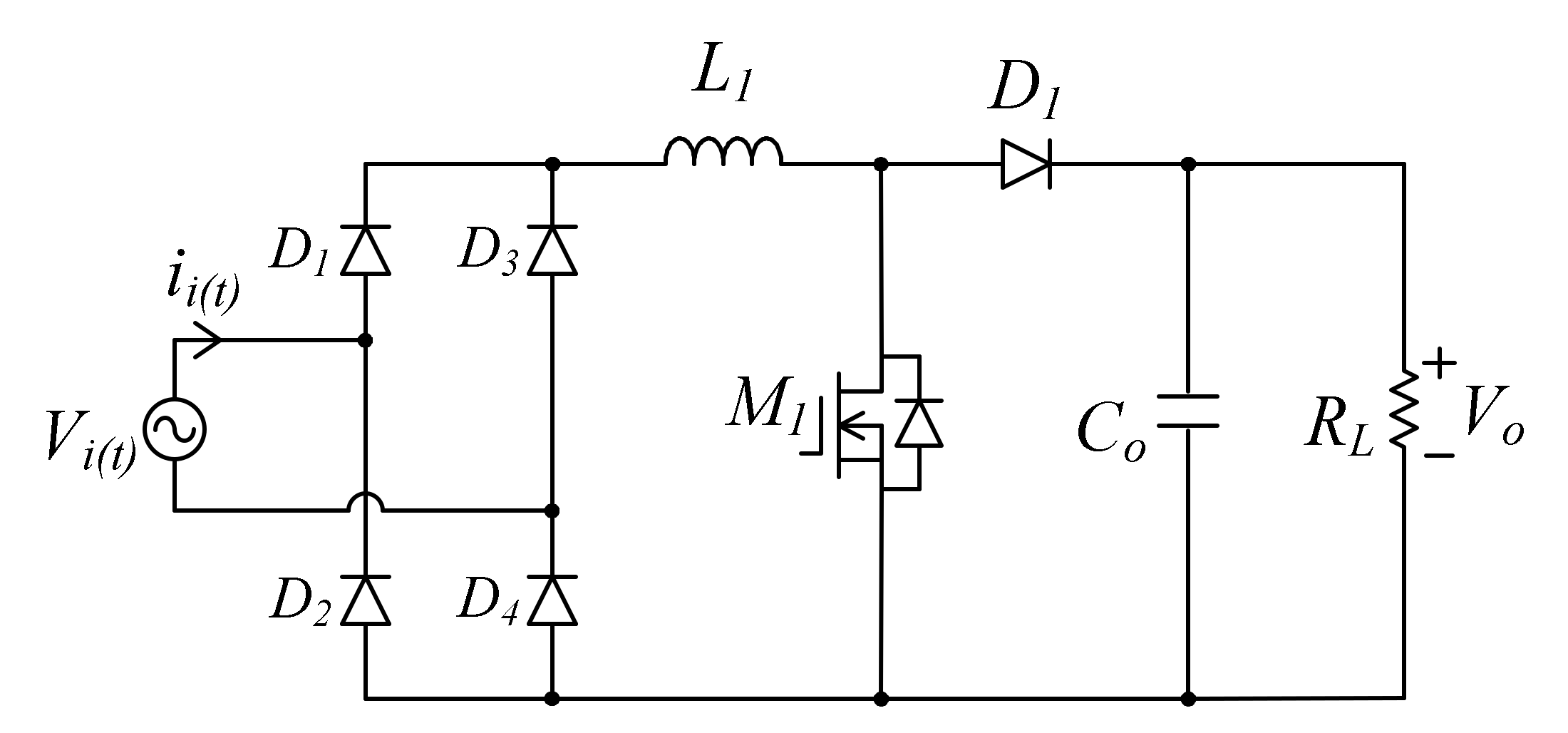
When an AC/DC power supply adopts active PFC to increase the PF, a boost converter is the most popular topology among the AC/DC converters. Since a boost converter is combined with a diode bridge rectifier to form the active PFC, losses from the diode bridge rectifier are significant, as shown in Figure 1. In particular, when the line source is at a lower input voltage and high output power, the conversion efficiency of the AC/DC converteris reduced. To improve the efficiency of the diode bridge rectifier, a bridgeless boost converter is adopted to reduce losses of diodes, as shown in Figure 2. Due to larger common-mode (CM) noise interference in the bridgeless boost converter shown in Figure 2, two diodes are added into the bridgeless boost converter, as shown in Figure 3. When the AC/DC converter adopts the modified bridgeless boost converter, the conversion efficiency of the AC/DC one can be reduced. In order to increase conversion efficiency, diodes DS1 and DS2 are replaced by switches MS1 and MS2, as illustrated in Figure 4. As mentioned above, the AC/DC converters using the conventional bridgeless boost converter can reduce the power losses of diodes and increase conversion efficiency.
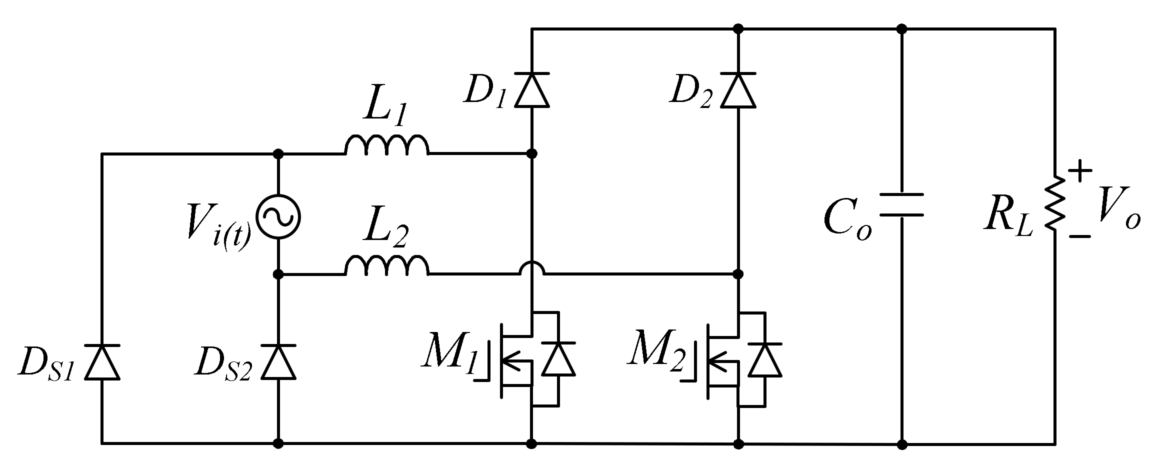
When a switching-mode converter is used in high-power applications, it will induce larger current ripples in input and output ports, resulting in a requirement for a larger passive filter. In order to reduce the passive component size, increase the output power level and decrease the current ripple, an interleaving circuit is usually adopted as an alternative solution in high-power applications. Many interleaving converters have been proposed, such as in [13,14,15,16,17,18,19]. When the AC/DC converter uses the conventional bridgeless boost converter for PFC applications, it can adopt its interleaving circuit to increase power processing capability, as shown in Figure 5. From Figure 5, it can be seen that the interleaving bridgeless boost converter can achieve a higher power factor, smaller current ripple and higher conversion efficiency. It is suitable for PFC applications.
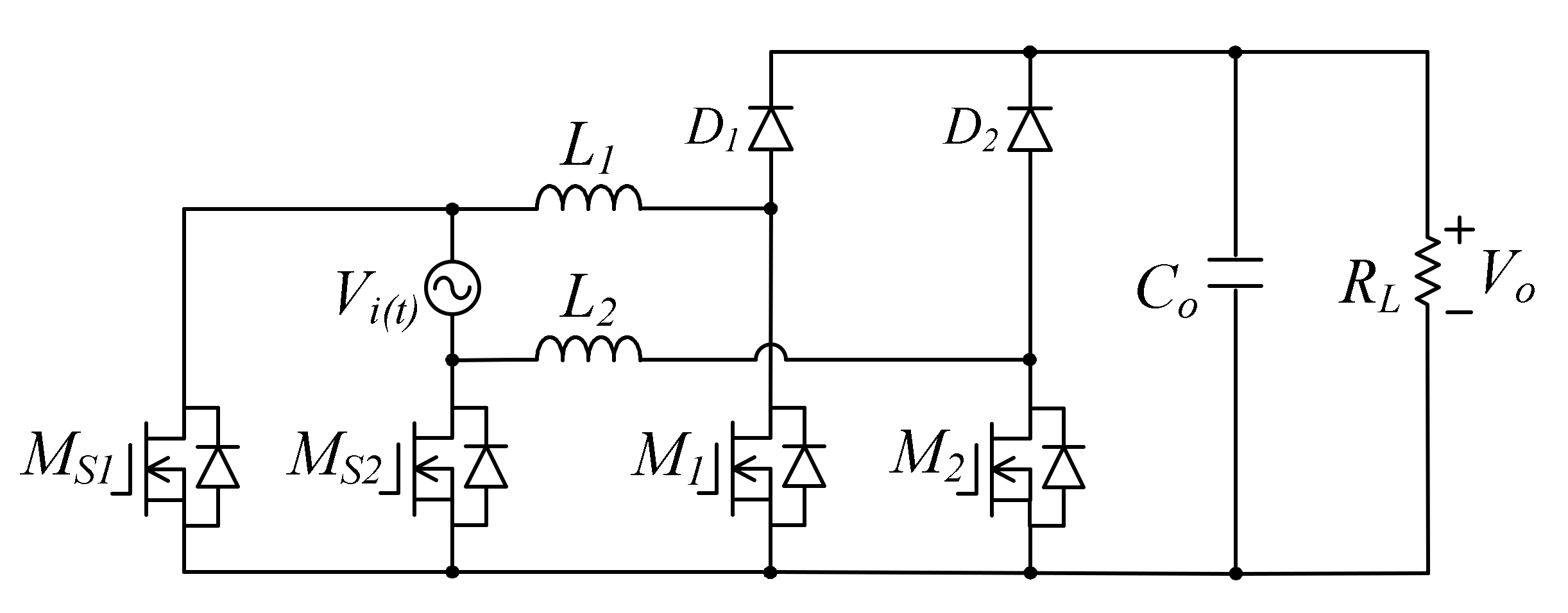
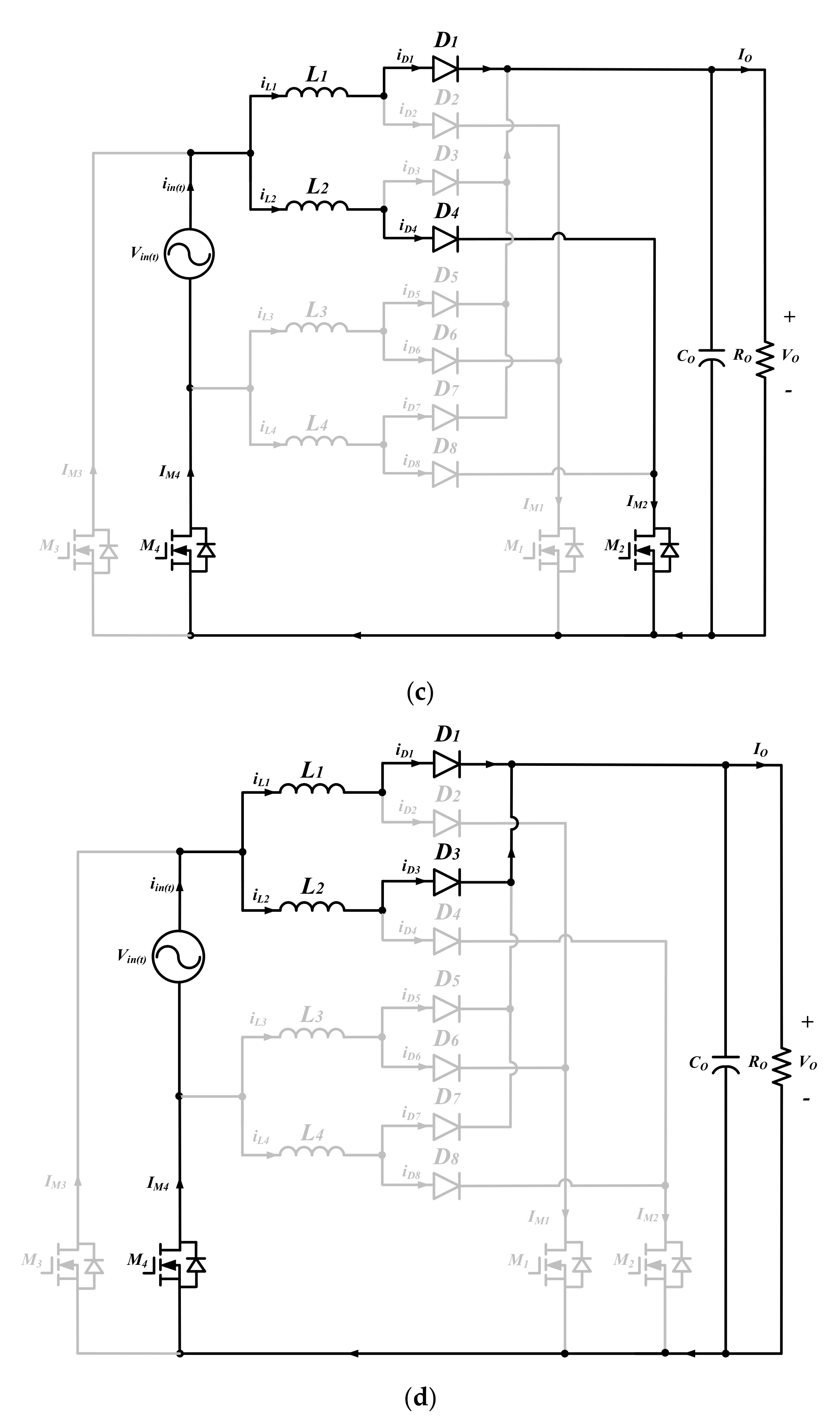
When PFC adopts the interleaving bridgeless boost converter illustrated in Figure 5, it needs a more complex driving circuit. In order to further simplify the circuit, switches M1~M4 shown in Figure 5 can be merged and replaced by switches M1 and M2, illustrated in Figure 6. According to performances of circuits shown in Figure 2, Figure 3, Figure 4, Figure 5 and Figure 6, each PFC circuit can be used in different situations. Table 1 shows the performance comparisons among different PFCs with power flow through component paths. When power flows through each component, it will generate power loss in the component, resulting in lower conversion efficiency. The circuits, shown in Figure 2, Figure 3 and Figure 4 are the single-phase topology. Their power level processing capability belongs in low- or medium-power applications. The circuits in Figure 5 and Figure 6 are the two-phase topology. Their power level processing capacities are suitable for medium- or high-power applications. In Table 1, it can be seen that the converter in Figure 4 possesses the highest conversion efficiency, while the one in Figure 3 has lower conversion efficiency. When the converter topology adopts a two-phase manner, the proposed boost converter can reduce component counts, resulting in lower conversion efficiency compared with the modified bridgeless boost converter with low CM noise shown in Figure 5. Their conversion efficiency difference is about 1%. Therefore, the proposed boost converter possesses superiority in PFC applications. In Figure 6, the proposed interleaving bridgeless boost converter can implement PFC functions and reduce current ripple and increase conversion efficiency and power processing capability.
2. Derivation of the Proposed Converter
Figure 5 shows a schematic diagram of the conventional interleaving bridgeless boost converter for PFC applications. Since the utility line source is divided into the positive half period and the negative half one, its power flow is different during each half period operation. When the conventional bridgeless boost converter is operated in the positive half period, switch Ms2 is turned on, and switches M1 and M2 are operated in an interleaving mode. If switches M1 and M2 are separately turned on, inductors L1 and L2, respectively, operate in the stored energy state. When switches M1 and M2 are separately operated in the turned-off state, inductors L1 and L2, respectively, operate in the released energy state through diodes D1 and D2. When the conventional bridgeless boost converter is operated in the negative half period, switch Ms1 is turned on, and switches M3 and M4 operate in the interleaving mode. Inductors L3 and L4 can be worked in the stored and released energy states, respectively, through switches M3 and M4 or diodes D3 and D4. According to the operations mentioned above, the conventional bridgeless boost converter can achieve PFC function.
In order to simplify the circuit shown in Figure 5, switches M2 and M4 are replaced by one switch, M2, and two diodes, D6 and D8, as shown in Figure 6. The switch M2 plays a switching role and is the same as that of switches M2 and M4 shown in Figure 5. Diodes D6 and D8 are used to avoid a reverse current from inductors L2 and L4, respectively. Moreover, switches M1 and M3 can be replaced by switch M1 and diodes D5 and D7, as shown in Figure 6. In Figure 6, it can be seen that switch M1 can be, respectively, operated in the positive half and the negative half periods to replace switches M1 and M3, shown in Figure 5, when inductors L1 and L3 are worked in the stored energy state. Diodes D5 and D7 are adopted to avoid the reverse currents of inductors L1 and L3, respectively. In addition, diodes D1 and D3 are, respectively, operated in the released energy states of inductors L1 and L3 when switch M1 is turned off.
3. Operational Principle of the Proposed Boost Converter
The proposed interleaving bridgeless boost converter is operated in a PFC manner. Its conceptual waveform is plotted in Figure 7 during a complete line period. When the proposed converter is operated during a complete line period, it can be divided into two operational periods: the positive and negative half periods. In the positive half period, switch M4 is turned on and switch M3 is turned off. In addition, switches M1 and M2 are operated in the interleaving manner. That is, their operation is out of phase by 180° for each switch. When the proposed converter operates in the negative half period, switch M3 is turned on and M4 is turned off. In the operational interval, switches M1 and M2 also operate in the interleaving manner. Since the operational principles of the proposed converter in the positive half period are the same as those in the negative half period, except that switch M4 turned on in the positive half periods changed to M3 turned on in the negative one, its operational principles are only described in this paper for the positive half period situation.
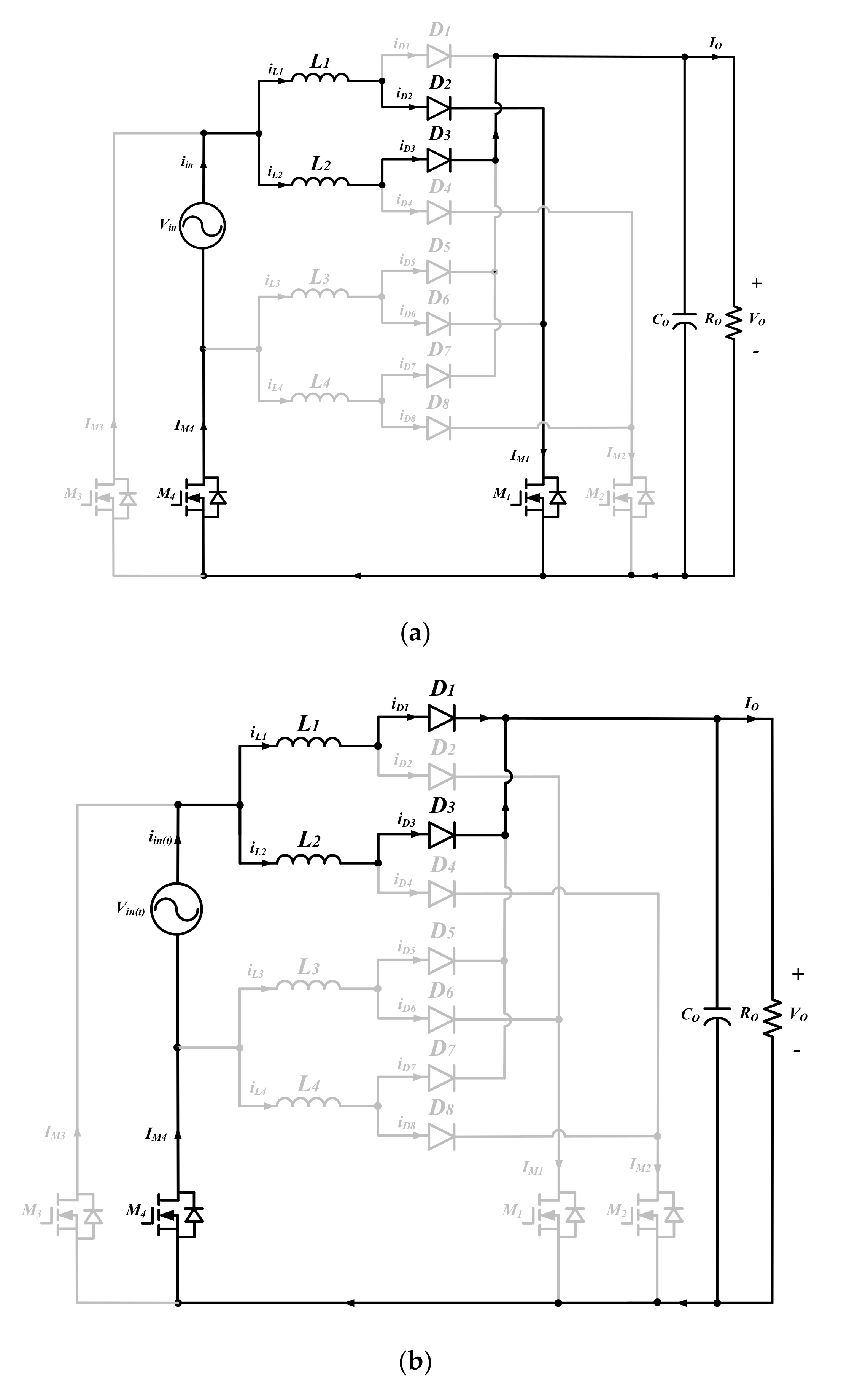
When the proposed interleaving boost converter is operated in the positive half period, input voltage varies from 0 V to a maximum value and then from the maximum value to 0 V with a sine wave variation. The duty ratio of the switch in the proposed converter slowly decreases its value, which depends on the level of increase in the input voltage. When the input voltage is high enough, the duty ratio is less than 0.5 and inductor currents iL1 and iL2 operate in continuous conduction mode (CCM). Its conceptual waveform is shown in Figure 7. According to the operational principle of the proposed converter, its operational mode is divided into four modes. The equivalent circuit of each operational mode is illustrated in Figure 8. Each operational mode of the proposed converter is briefly described in the following section.
Mode 1 (Figure 8a: t0 ≤ t < t1): Before t0, inductors L1 and L2 simultaneously work in the released energy states. Diodes D1 and D2 are forwardly biased. Currents iL1 and iL2 linearly decrease through D1, load R0 and switch M4, and D3, load R0 and switch M4, respectively. When t = t0, switch M1 is turned on and M4 is kept in a turned-on condition. Diode D1 is reversely biased and D2 is forwardly biased, and inductor L1 enters the stored energy state. In addition, inductor L2 works in the released energy state through diode D3. During this interval, inductor current iL1 linearly increases and current iL2 linearly decreases.
Mode 2 (Figure 8b: t1 ≤ t < t2): At t1, switch M1 is turned off and M2 is still in a turned-off state. Inductors L1 and L3 are in the released energy state through diodes D1, D3 and switch M4, simultaneously. In this mode, currents iL1 and iL2 linearly decrease.
Mode 3 (Figure 8c: t2 ≤ t < t3): When t = t2, switch M2 is turned on and M4 is kept in the turned-on state. Inductor L2 operates in the stored energy state through diode D4 and switch M4. Therefore, inductor current iL1 linearly decreases and iL2 linearly increases.
Mode 4 (Figure 8d: t3 ≤ t < t4): At t = t3, switch M2 is turned off. Inductor L2 changes the operation state from the stored energy state to the released energy state. Diodes D1 and D3 help inductors L1 and L2 turn to the released energy state, respectively. During this interval, currents iL1 and iL2 linearly decrease. When t = t4, switch M1 is turned on again. The new switching cycle starts.
4. Design of the Proposed Interleaving Bridgeless Boost Converter
The proposed interleaving bridgeless boost converter adopts the interleaving circuit to reduce input and output ripple currents. Its inductor ripple cancellation k(D) is derived in this paper. For the design of the proposed converter, the determination of duty ratio D, inductors L1~L4 and output capacitor C0 is important. In addition, the selection of components D1~D8, M1~M4 is also described in this paper. Their design is briefly derived as follows.
- (a)
- Ripple current cancellation K(D)
The proposed interleaving boost converter can reduce the ripple currents of inductors L1~L4. The ratio K(D) of input ripple current Δiin to individual inductor ripple current ΔiL1 in the interleaving boost converter is plotted in Figure 9. When duty ratio D is equal to or less than 0.5, K(D) can determined by
If D is greater than 0.5, K(D) can be derived by
According to (1) and (2), when D = 0.5, K(D) = 0, input ripple current Δiin is equal to 0 A.
- (b)
- Duty ratio D
The input voltage range of the proposed boost converter is from AC 90 V to AC 265 V. When the input voltage is at low line, the duty ratio can be obtained by
where Vin-min represents AC 90 V. If the input voltage is at high line, duty ratio DPHL can determined as
where Vin-max is equal to AC 265 V. Duty ratio D can be varied from DPHL to DPLL.
- (c)
- Inductors L1~L4
Since the maximum inductor current iL(max) is at low line of the input voltage, inductors L1~L4 can be determined for control within a desired range. In order to determine the values of inductors L1~L4, the ripple current ΔiL must be specified. When the proposed boost converter is operated at low line, ΔiL(max) can be obtained by
where 0.3 means that the maximum input ripple current was set to 30% of the peak input current at low line, η represents the conversion efficiency under a full-load condition and K(DPLL) is the ratio of input current to inductor ripple current at the peak of low line operation. When ΔiL(max) is determined, inductor L1(=L2=L3=L4) can be obtained as
where Ts is the switching period.
- (d)
- Output capacitor Co
When the proposed boost converter is applied to PFC applications, output capacitor Co must sustain the output voltage Vo at a desired value during loss of the line source under one line cycle. In general, when the line source faulty is during a line cycle, output voltage Vo can be kept at and be greater than 0.75Vo. According to the above requirement, output capacitor Co can be derived as
where fl is the line frequency of the line source, and when output capacitor Co is determined, output ripple voltage ΔVo can be expressed by
where ωl is equal to 2πfl.
- (e)
- Selection of switches and diodes
Figure 6 shows the schematic diagram of the proposed interleaving bridgeless boost converter. In order to determine the voltage and current ratings of components, the input voltage is in different situations. When the input voltage is in a high line situation, the voltage ratings of components in the proposed converter can be determined. The maximum voltage stresses of switches M1 and M2 can be determined by
In addition, that of diodes D1~D8 can be expressed by
In a high line situation, the voltage stresses of switches M3 and M4 can be obtained: as
where Vin(max) represents the input voltage level in a high line situation. When the input voltage is in a low line condition, rms currents IM1(rms) (=IM2(rms)) of switch M1 can be derived as
where Po is the maximum output power, Vin-min represents the rms value of input line voltage in a low line condition, η is the conversion efficiency of the proposed converter and Vo is the output voltage. Switch rms currents IM3(rms) (= IM4(rms)) can be expressed by
Additionally, the diode rms current iD1(rms)( = iD2(rms) = iD3(rms) = iD4(rms)) is derived as
The diode rms current iD5(rms)( = iD6(rms) = iD7(rms) = iD8(rms)) is derived by
Furthermore, the output capacitor rms current ICo(rms) is shown by
5. Experimental Results
The proposed interleaving bridgeless boost converter is shown in Figure 6. In order to verify the performance of the proposed converter, a prototype with the following specifications was implemented.
- Input voltage Vin: AC 90 V~265 V,
- Switching frequency fs: 65 kHz,
- Output voltage Vo: 400 V,
- Maximum output current Io(max): 2.5 A and
- Maximum output power Po(max): 1 kW.
According to the equations mentioned above, the design values of key components of the proposed converter are listed in Table 2. The practical components are shown in the following section.
- Switches M1~M4: IRFP460,
- Diodes D1~D8: C3D10060,
- Inductances L1~L4: 210 μH and
- Capacitor Co: 1880 μF/450 V.
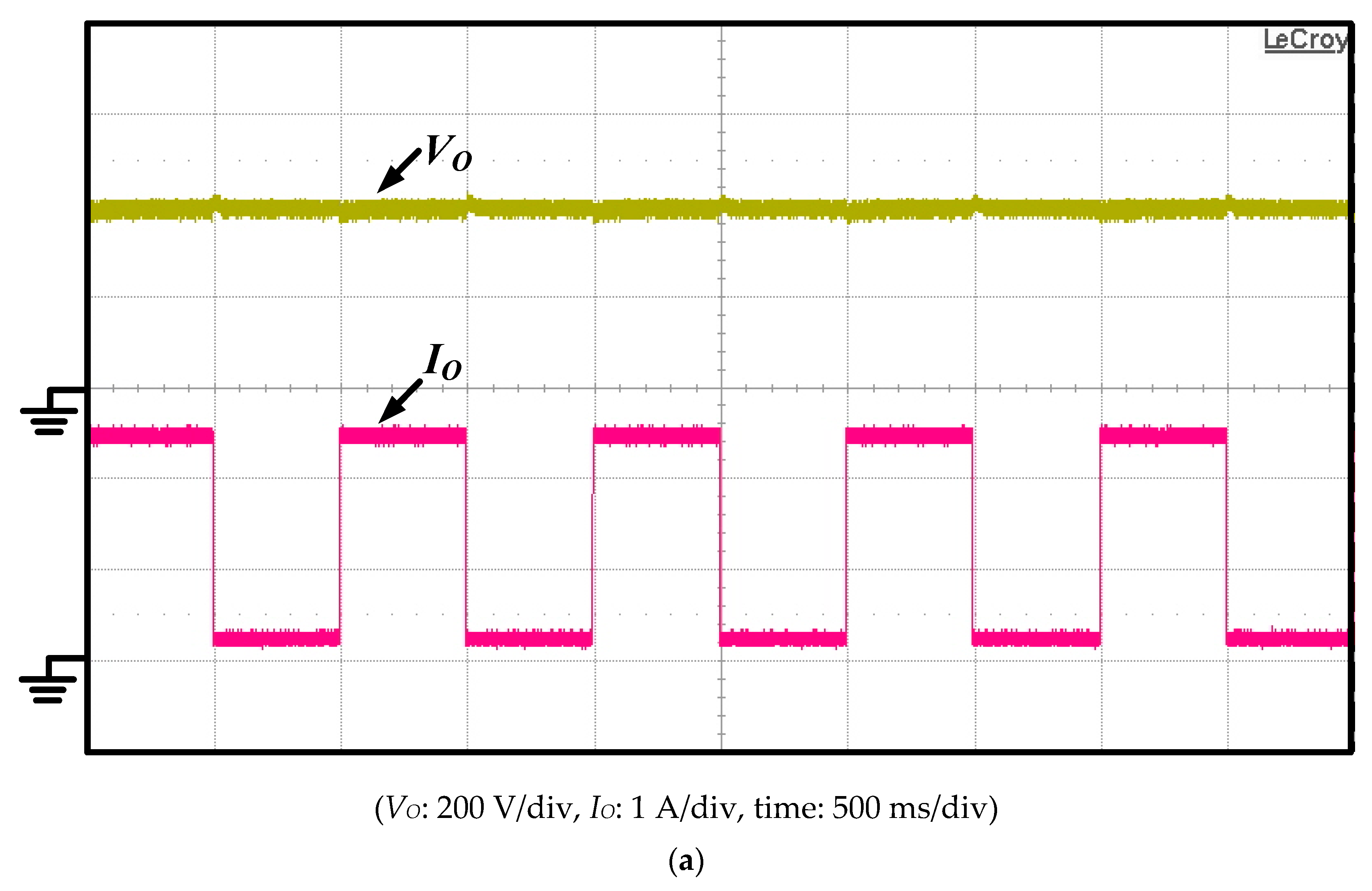
The proposed interleaving bridgeless boost converter is proposed to achieve a higher PF and a lower input ripple current. Figure 10 shows the measured currents iL1, iL2 and iin waveforms of the proposed interleaving bridgeless converter under AC 90 V of input voltage. Figure 10a shows those waveforms with 10% of the full-load condition, while Figure 10b illustrates those waveforms with 100% of the full-load condition. In Figure 10, it can be seen that the proposed converter operates in discontinuous conduction mode (DCM) under 10% of the full-load condition, and operates in CCM under 100% of the full-load condition. Furthermore, the input ripple current can be reduced from a light load to a heavy load. Measured output voltage Vo and current Io waveforms of step-load changes between 10% and 100% of the full-load condition with a duty ratio of 50% and a repetitive period of 1s are illustrated in Figure 11. Figure 11a depicts those waveforms under AC 220 V of the input voltage. From Figure 11, output voltage Vo is regulated within a desired voltage range. Its value is limited within 1%.
The conversion efficiency of the proposed boost converter from a light load to a heavy load under the different input voltage is plotted in Figure 12. In Figure 12, when the input voltage is at a higher level, its conversion efficiency is higher than that of a lower input voltage from a light load to a heavy load. The maximum conversion efficiency is 96% under 80% of the full-load condition at AC 230 V of input voltage. From Figure 12, it can be seen that the conversion efficiency of the proposed boost converter is higher than 88% under different input voltages. Since the input voltage Vin varies with the sine wave, it is difficult to evaluate the power loss of each component with an accurate method. In general, power loss analysis of PFC is usually adopted by simulation tools to obtain approximate power losses for the converter. Table 3 lists the parameters of selection components in the proposed boost converter. According to Equations (12)–(16), the rms currents of switches and diodes can be obtained from a light load to a heavy load at input voltage Vin of AC 110 V. Table 4 shows the power loss of each semiconductor. In Table 4, power losses of switches include switching loss and conduction loss. Figure 13 shows the conceptual waveforms of switching loss during switch turn-on and turn-off transitions. In addition, the conduction loss of switches can be determined by , where IM(rms) is the average rms current of a switch and Rds(on) expresses the resistance of a switch in the conduction state. Power loss analysis of diodes is evaluated by ID(rms)VF, where ID(rms) is the average rms current of a diode and VF is its forward drop voltage. Switches M3 and M4 are turned on or turned off at the zero-crossing point. Therefore, their switching losses are equal to 0. Their power losses only consider conduction loss.
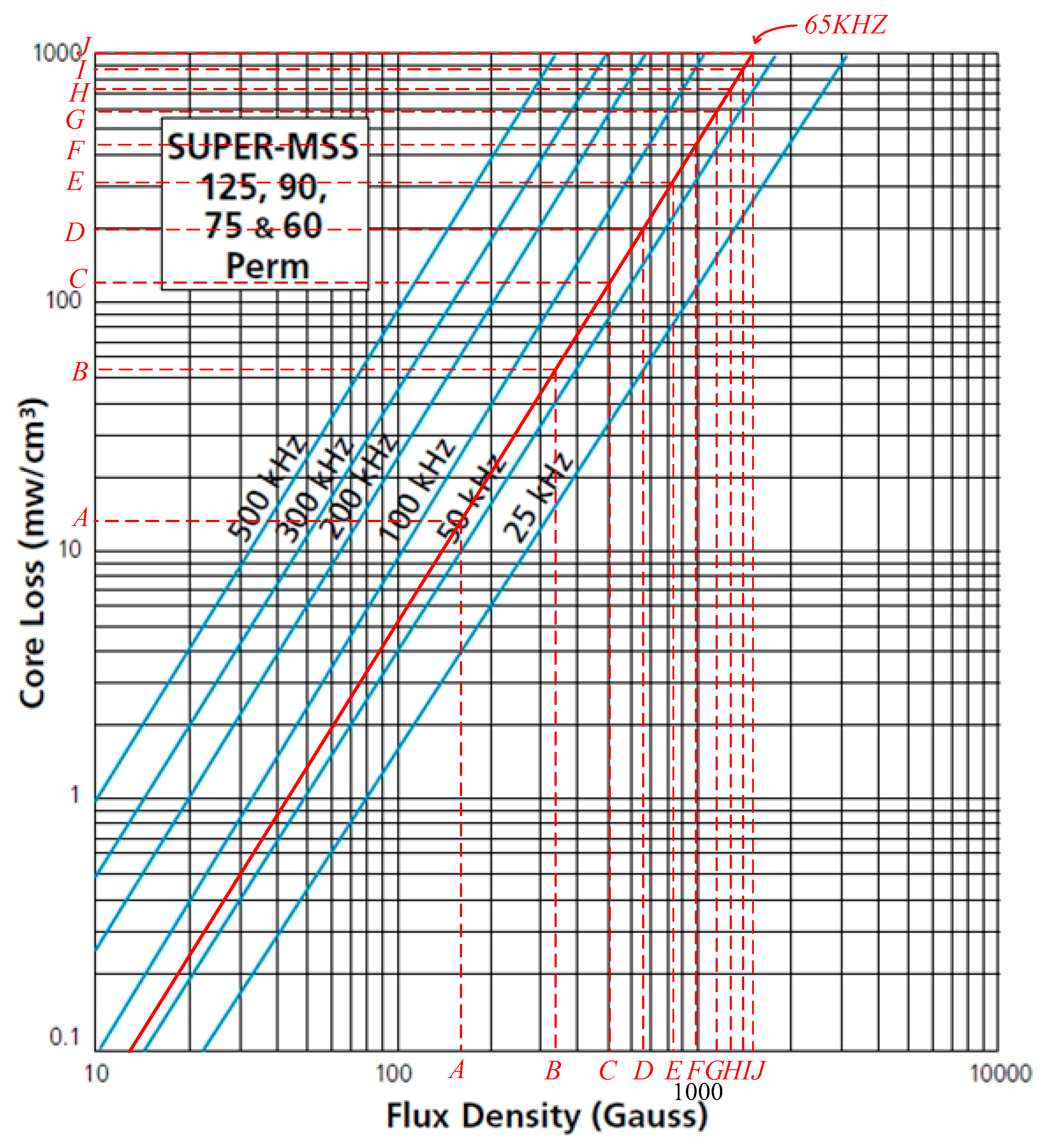
In the proposed boost converter, a major power loss is core loss Pc and copper loss Pcp in the inductors. Table 5 illustrates core loss Pc and copper loss Pcp of inductors L1~L4 of the proposed boost converter. Since inductors L1~L4 in the proposed boost converter are selected with super-MSS powder core manufactured by Arnold Magnetics LTD, its core loss curves are shown in Figure 14. The core loss must first obtain maximum flux density Bm, and then the core loss coefficient is determined, which is specified by Figure 14. Moreover, copper loss can be determined by , in which Rdc is the resistance of wire gauge. Table 6 illustrates the power loss analysis of the proposed boost converter under input voltage Vin of AC110V. According to Table 6, it can be seen that when output power Po is less than 40% of the maximum output power Po(max), the calculation efficiency ηc is higher than practical efficiency ηp. The reason for is that the stray losses do not include in the total power losses of the proposed converter, resulting in a lower practical efficiency. When output power Po is greater than 40% of the full-load condition, the proposed converter operates in CCM. Its practical peak currents of switches and inductors are less than those with the calculation method. Therefore, core losses of inductors and switching losses of switches with the calculation method are greater than the practical losses, meaning that the calculation efficiency ηc is less than that of the practical efficiency ηp. Their difference is 2–3%. The calculation efficiency can be regarded as the reference efficiency.
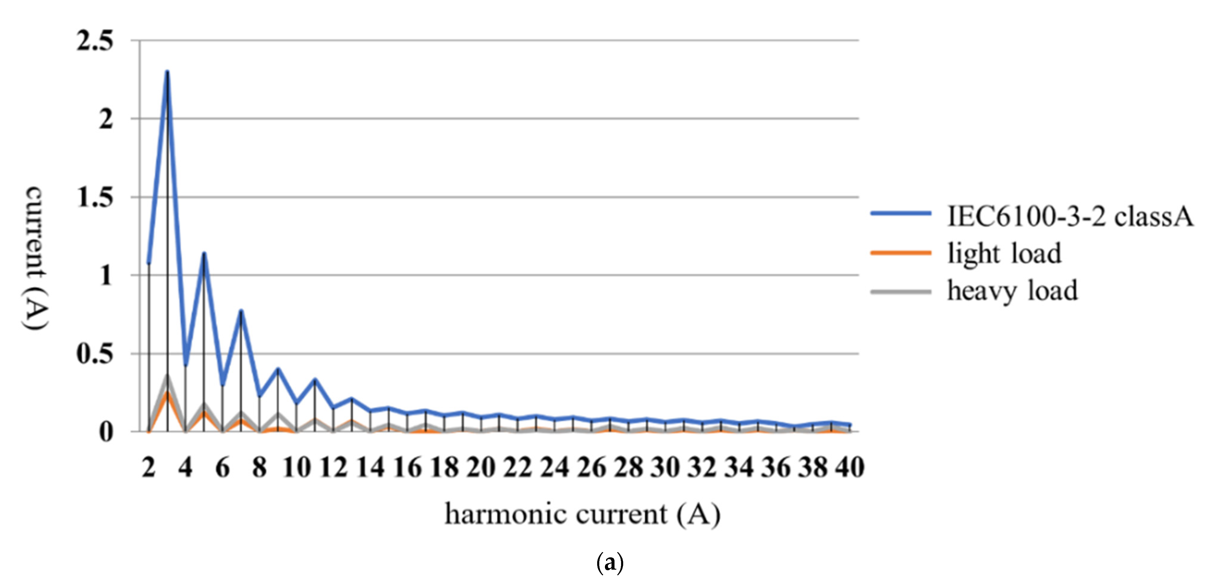
Figure 15 shows plots of the harmonic current of the proposed boost converter from a light load to a heavy load at different input voltages. From Figure 15, it can be seen that the harmonic current of the proposed converter from a light load to a heavy load under different input voltages can meet the requirements of IEC-6100-3-2 class A. In addition, plots of the power factor of the proposed converter from a light load to a heavy load under different input voltages are illustrated in Figure 16. With different input voltages, the power factor of the proposed converter from a light load to a heavy load is higher than 0.8. As mentioned above, the proposed interleaving bridgeless boost converter can implement a lower input ripple current, a higher conversion efficiency and a higher power factor. It is suitable for PFC applications.
6. Conclusions
The proposed interleaving bridgeless boost converter is presented for PFC applications. The proposed converter adopts interleaving and bridgeless circuits to increase the power process capability and increase conversion efficiency, simultaneously. In this paper, the operational principle and design of the proposed converter have been described in detail. According to the experimental results of the proposed converter, input ripple current can be reduced and power factor can be increased. Furthermore, the proposed converter can also achieve a lower harmonic current and a higher conversion efficiency. Its harmonic current from a light load to a heavy load under different input voltages can meet the requirements of IEC-6100-3-2 class A. The maximum conversion efficiency is about 96.4% under 80% of the full-load condition at AC 265 V of input voltage. In addition, the power factor from a light load to a heavy load under different input voltages is higher than 0.8. From the experimental results of the proposed interleaving bridgeless boost converter mentioned above, the proposed converter was implemented to verify its feasibility. It is suitable for PFC applications.
Author Contributions
Conceptualization, methodology, and writing—original draft preparation, S.-Y.T.; writing—review and editing, J.-H.F. All authors have read and agreed to the published version of the manuscript.
Funding
This research was funded by MOST in Taiwan, grant number MOST 109-2221-E-182-005.
Conflicts of Interest
The authors declare no conflict of interest.
References
- Li, Q.; Wolfs, P.J. A Review of the Single Phase Photovoltaic Module Integrated Converter Topologies with Three Different DC Link Configurations. IEEE Trans. Power Electron. 2008, 23, 1320–1333. [Google Scholar] [CrossRef] [Green Version]
- Muyeen, S.M.; Takahashi, R.; Murata, T.; Tamura, J. A variable speed wind turbine control strategy to meet wind farm grid code requirements. IEEE Trans. Power Electron. 2010, 25, 331–340. [Google Scholar] [CrossRef]
- Nejabatkhah, F.; Danyali, S.; Hosseini, S.H.; Sabahi, M.; Niapour, S.M. Modeling and Control of a New Three-Input DC–DC Boost Converter for Hybrid PV/FC/Battery Power System. IEEE Trans. Power Electron. 2012, 27, 2309–2324. [Google Scholar] [CrossRef]
- Matsuo, H.; Lin, W.; Kurokawa, F.; Shigemizu, T.; Watanabe, N. Characteristicsof the multi-input dc-dc converter. IEEE Trans. Ind. Electron. 2004, 51, 625–631. [Google Scholar] [CrossRef]
- Li, Y.-C.; Chen, C.-L. A Novel Primary-Side Regulation Scheme for Single-Stage High-Power-Factor AC–DC LED Driving Circuit. IEEE Trans. Ind. Electron. 2012, 60, 4978–4986. [Google Scholar] [CrossRef]
- Tsai, H.-Y.; Hsia, T.-H.; Chen, D. A family of zero-voltagetransition bridgeless power-factor-correction circuits with a zero-currentswitching auxiliary switch. IEEE Trans. Ind. Electron. 2011, 58, 1848–1855. [Google Scholar] [CrossRef]
- Nassary, M.; Orabi, M.; Ghoneima, M. Discussion of Single-Stage Isolated Unidirectional AC-DC On-Board Battery Charger for Electric Vehicle. In Proceedings of the 2018 IEEE 4th Southern Power Electronics Conference (SPEC), Singapore, 10–13 December 2018; pp. 1–7. [Google Scholar]
- Wang, H.; Dusmez, S.; Khaligh, A. Design and Analysis of a Full-Bridge LLC-Based PEV Charger Optimized for Wide Battery Voltage Range. IEEE Trans. Veh. Technol. 2014, 63, 1603–1613. [Google Scholar] [CrossRef]
- Mahdavi, M.; Farzanehfard, H. Zero-voltage transition bridgeless single-ended primary inductance converter power factor correction rectifier. IET Power Electron. 2014, 7, 895–902. [Google Scholar] [CrossRef] [Green Version]
- Shin, J.-W.; Choi, S.-J.; Cho, B.-H. High-Efficiency Bridgeless Flyback Rectifier with Bidirectional Switch and Dual Output Windings. IEEE Trans. Power Electron. 2013, 29, 4752–4762. [Google Scholar] [CrossRef]
- Bist, V.; Singh, B. An Adjustable-Speed PFC Bridgeless Buck–Boost Converter-Fed BLDC Motor Drive. IEEE Trans. Ind. Electron. 2013, 61, 2665–2677. [Google Scholar] [CrossRef]
- Electromagnetic Compatibility (EMC)-Part 3-2: Limits for Harmonic Current Emissions (Equipment Input Current <16 A per Phase); Document IEC 61000-3-2; International Electrotechnical Commission: Geneva, Switzerland, 2018; Available online: https://webstore.iec.ch/publication/28164 (accessed on 20 January 2021).
- Muhammad, M.; Armstrong, M.; Elgendy, M.A. A Nonisolated Interleaved Boost Converter for High-Voltage Gain Applications. IEEE J. Emerg. Sel. Top. Power Electron. 2015, 4, 352–362. [Google Scholar] [CrossRef] [Green Version]
- Musavi, F.; Eberle, W.; Dunford, W.G. A High-Performance Single-Phase Bridgeless Interleaved PFC Converter for Plug-in Hybrid Electric Vehicle Battery Chargers. IEEE Trans. Ind. Appl. 2011, 47, 1833–1843. [Google Scholar] [CrossRef]
- Yang, F.; Ruan, X.; Yang, Y.; Ye, Z. Interleaved Critical Current Mode Boost PFC Converter with Coupled Inductor. IEEE Trans. Power Electron. 2011, 26, 2404–2413. [Google Scholar] [CrossRef]
- Marxgut, C.; Biela, J.; Kolar, J.W. Interleaved Triangular Current Mode (TCM) resonant transition, single phase PFC rectifier with high efficiency and high power density. In Proceedings of the 2010 International Power Electronics Conference—ECCE ASIA, Sapporo, Japan, 21 June 2010; pp. 1725–1732. [Google Scholar]
- Huang, Q.; Huang, A.Q. Review of GaN Totem-Pole Bridgeless PFC. CPSS Trans. Power Electron. 2017, 2, 187–196. [Google Scholar] [CrossRef]
- Park, M.H.; Baek, J.; Jeong, Y.; Moon, G.W. An Interleaved Totem-Pole Bridgeless Boost PFC Converter with Soft-Switching Capability Adopting Phase-Shifting Control. IEEE Trans. Power Electron. 2019, 34, 10610–10618. [Google Scholar] [CrossRef]
- Huang, L.; Chen, F.; Yao, W.; Lu, Z. Flexible Mode Bridgeless Boost PFC Rectifier with High Efficiency Over a Wide Range of Input Voltage. IEEE Trans. Power Electron. 2016, 32, 3513–3524. [Google Scholar] [CrossRef]
Figure 1.
Schematic diagram of boost converter for power factor corrector (PFC) applications.

Figure 2.
Schematic diagram of the bridgeless boost converter without low common-mode (CM) noise for PFC applications.
Figure 2.
Schematic diagram of the bridgeless boost converter without low common-mode (CM) noise for PFC applications.

Figure 3.
Schematic diagram of the bridgeless boost converter with low CM noise for PFC applications.
Figure 3.
Schematic diagram of the bridgeless boost converter with low CM noise for PFC applications.

Figure 4.
Schematic diagram of the modified bridgeless boost converter with low CM noise for PFC applications.
Figure 4.
Schematic diagram of the modified bridgeless boost converter with low CM noise for PFC applications.

Figure 5.
Schematic diagram of the modified interleaving bridgeless boost converter with a low CM noise for PFC applications.
Figure 5.
Schematic diagram of the modified interleaving bridgeless boost converter with a low CM noise for PFC applications.

Figure 6.
Schematic diagram of the proposed interleaving bridgeless boost converter.

Figure 7.
Conceptual waveforms of the proposed interleaving bridgeless boost converter during a complete line period.
Figure 7.
Conceptual waveforms of the proposed interleaving bridgeless boost converter during a complete line period.

Figure 8.
Equivalent circuit of the proposed interleaving bridgeless boost converter operated in the positive half period over one switching cycle. (a) Mode 1 (t0 ≤ t ≤ t1), (b) Mode 2 (t1 ≤ t < t2), (c) Mode 3 (t2 ≤ t < t3), (d) Mode 4 (t3 ≤ t < t4).
Figure 8.
Equivalent circuit of the proposed interleaving bridgeless boost converter operated in the positive half period over one switching cycle. (a) Mode 1 (t0 ≤ t ≤ t1), (b) Mode 2 (t1 ≤ t < t2), (c) Mode 3 (t2 ≤ t < t3), (d) Mode 4 (t3 ≤ t < t4).


Figure 9.
Plot of input inductor ripple current cancellation curve.

Figure 10.
Measured currents iL1 and iL2 and iin waveforms of the proposed interleaving boost converter with (a) 10% of full-load condition, and (b) 100% of full-load condition under AC 90V of input voltage.
Figure 10.
Measured currents iL1 and iL2 and iin waveforms of the proposed interleaving boost converter with (a) 10% of full-load condition, and (b) 100% of full-load condition under AC 90V of input voltage.


Figure 11.
Measured output voltage Vo and current Io waveforms of step-load changes between 10% and 100% of full-load conditions with duty ratio of 50% and repetitive period of 1 s: (a) under AC 110 V of input voltage, and (b) under AC 220 V of input voltage.
Figure 11.
Measured output voltage Vo and current Io waveforms of step-load changes between 10% and 100% of full-load conditions with duty ratio of 50% and repetitive period of 1 s: (a) under AC 110 V of input voltage, and (b) under AC 220 V of input voltage.


Figure 12.
Plots of conversion efficiency of the proposed interleaving boost converter from light load to heavy load under the different input voltages.
Figure 12.
Plots of conversion efficiency of the proposed interleaving boost converter from light load to heavy load under the different input voltages.

Figure 13.
Conceptual waveforms of switching loss during (a) a complete switching cycle (b) switch turn-on transition, and (c) turn-off transition.
Figure 13.
Conceptual waveforms of switching loss during (a) a complete switching cycle (b) switch turn-on transition, and (c) turn-off transition.

Figure 14.
Core loss curves of inductors L1~L4manufactured by Arnold Magnetics LTD.

Figure 15.
Plots of harmonic current of the proposed interleaving bridgeless boost converter from light load to heavy load (a) under input voltage of 110 V, and (b) under input voltage of 220 V.
Figure 15.
Plots of harmonic current of the proposed interleaving bridgeless boost converter from light load to heavy load (a) under input voltage of 110 V, and (b) under input voltage of 220 V.


Figure 16.
Plots of the power factor of the proposed interleaving bridgeless boost converter from light load to heavy load under different input voltages.
Figure 16.
Plots of the power factor of the proposed interleaving bridgeless boost converter from light load to heavy load under different input voltages.


Table 1.
Performance comparison among different PFCs with power flow through component paths.
| Performances or Operational States | Power Flow through Component Paths | |||||
|---|---|---|---|---|---|---|
| Figure 2 Single Phase | Figure 3 Single Phase | Figure 4 Single Phase | Figure 5 Two Phase | Figure 6 Two Phase | ||
| The positive half period | inductor in the stored energy state | , , | , | , | , | , , |
| , | , , | |||||
| inductor in the released energy state | , , | , | , | , | , | |
| , | , | |||||
| The negative half period | inductor in the stored energy state | , , | , | , | , | , , |
| , | , , | |||||
| inductor in the released energy state | , , | , | , | , | , | |
| , | , | |||||
| Power level processing capability | small | small | small | large | large | |
| Input and output current ripple | large | large | large | small | small | |
| Efficiency | higher | low | highest | highest | higher | |
Table 2.
Parameters of components in the proposed boost converter.
| Symbol | Calculation Value | Practical Value | Relevant Parameters | |
|---|---|---|---|---|
| Equation | Value | |||
| (3) | 0.70 | ; | ||
| K() | (2) | 0.57 | ||
| Δ | (5) | 9.73 A | 6.16 A | K() = 0.57; ; η = 0.9 |
| (6) | 133 µH | 210 µH | ; µs; Δ= 9.73 A | |
| (7) | 476 µF | 1880 µF | ; ; | |
| Δ | (8) | 13.94 V | 3.53 V | ; |
| (9) | 400 V | 500 V | ||
| (10) | 400 V | 600 V | ||
| (11) | 375 V | 500 V | ||
| (12) | 5.64 A | 20 A | M1~M4:IRFP460 (500 V/20 A) D1~D8:C3D10060 (600 V/10 A) ; Η = 0.9; | |
| (13) | 6.54 A | 20 A | ||
| (14) | 2.34 A | 10 A | ||
| (15) | 3.99 A | 10 A | ||
| (16) | 3.94 A | |||
Table 3.
Key component parameters of the proposed converter.
| Component | Part Number | Voltage/Current Ratingsor Formula | Features | ||
|---|---|---|---|---|---|
| Symbol | Parameter | Values | |||
| M1, M2 M3, M4 | IRFP640 | 500 V/20 A | Drain–source turn-on resistance | 0.2~0.27 Ω | |
| Turn-on transition time | 104 ns | ||||
| Turn-off transition time | 150 ns | ||||
| ~ | C3D10060 | 600 V/10 A | Forward voltage | 1.5 V | |
| ~ | Arnold MS-184060-2 | : 4π* N: Turns : Effective Magnetic Path Length(m) : Peak Current (A) | Permeability | 60 | |
| Outside diameter | 46.74 mm | ||||
| Inside diameter | 24.13 mm | ||||
| Height | 18.03 mm | ||||
| Effective cross sectional area | 1.990 | ||||
| Effective magnetic path length | 10.743 cm | ||||
| Effective core volume | 21.373 | ||||
| Approximate mean length of turn | 6.16 cm | ||||
| N | Turns | 32 | |||
| AWG#18 | Wire gauge | Diameter 1.0 mm | |||
| : resistance | 21.4 mΩ/m | ||||
Table 4.
Semiconductor loss analysis for the proposed boost converter under input voltage of AC 100 V.
Table 4.
Semiconductor loss analysis for the proposed boost converter under input voltage of AC 100 V.
| Load (%) | Efficiency η (%) | |||||
|---|---|---|---|---|---|---|
| Switching Loss () (w) | Conduction Loss (w) | Conduction Loss (w) | Forward Drop Voltage Loss (w) | Forward Drop Voltage Loss (w) | ||
| 10 | 90 | 1.38 | 0.03 | 0.025 | 0.55 | 0.88 |
| 20 | 91 | 2.75 | 0.13 | 0.1 | 1.11 | 1.74 |
| 30 | 92.5 | 4.08 | 0.29 | 0.22 | 1.64 | 2.57 |
| 40 | 93 | 5.38 | 0.51 | 0.38 | 2.18 | 3.40 |
| 50 | 93.5 | 6.71 | 0.79 | 0.59 | 2.7 | 4.23 |
| 60 | 94 | 8.0 | 1.13 | 0.84 | 3.23 | 5.04 |
| 70 | 94.5 | 9.28 | 1.52 | 1.14 | 3.74 | 5.85 |
| 80 | 94.5 | 10.61 | 2.0 | 1.48 | 4.3 | 6.70 |
| 90 | 94 | 12.02 | 2.55 | 1.89 | 4.8 | 7.58 |
| 100 | 93 | 13.48 | 3.22 | 2.39 | 5.43 | 8.51 |
Table 5.
Parameters of core and core loss analysis for the proposed converter.
| Load (%) | Efficiency η (%) | Input Current rms (A) | Core Loss and Parameters of Core | |||||
|---|---|---|---|---|---|---|---|---|
(N = 32T) (w) | ||||||||
| 10 | 90 | 1.01 | 0.35 | 0.71 | 171.2 G | 13 | 0.14 | ≒5.17 m |
| 20 | 91 | 2.0 | 0.7 | 1.41 | 340.02 G | 50 | 0.53 | ≒20.67 m |
| 30 | 92.5 | 2.95 | 1.03 | 2.09 | 504.01 G | 120 | 1.28 | ≒44.75 m |
| 40 | 93 | 3.91 | 1.37 | 2.76 | 665.58 G | 200 | 2.14 | ≒79.17 m |
| 50 | 93.5 | 4.86 | 1.70 | 3.44 | 829.56 G | 300 | 3.20 | 0.122 |
| 60 | 94 | 5.80 | 2.03 | 4.10 | 988.72 G | 420 | 4.49 | 0.173 |
| 70 | 94.5 | 6.73 | 2.36 | 4.76 | 1147.88 G | 580 | 6.2 | 0.235 |
| 80 | 94.5 | 7.7 | 2.70 | 5.44 | 1311.87 G | 710 | 7.59 | 0.307 |
| 90 | 94 | 8.7 | 3.05 | 6.15 | 1843.08 G | 860 | 9.19 | 0.392 |
| 100 | 93 | 9.78 | 3.42 | 6.91 | 1666.36 G | 980 | 10.47 | 0.493 |
Table 6.
Power loss analysis for the proposed boost converter under input voltage of AC 110 V.
| Load (%) | Efficiency ηp (%) | Switch Losses | Diode Losses | Total Core Losses | Total Power Losses | Calculation Efficiency ηc (%) | ||
|---|---|---|---|---|---|---|---|---|
(w) | ||||||||
| 10 | 90 | 2.82 | 0.05 | 2.2 | 3.52 | 0.56 | 9.15 | 9.16 |
| 20 | 91 | 5.76 | 0.2 | 2.22 | 3.48 | 2.12 | 13.78 | 93.6 |
| 30 | 92.5 | 8.74 | 0.44 | 3.28 | 5.14 | 5.12 | 22.72 | 93 |
| 40 | 93 | 11.76 | 0.76 | 4.36 | 6.8 | 8.56 | 32.24 | 92.5 |
| 50 | 93.5 | 15 | 1.18 | 5.4 | 8.46 | 13.28 | 43.32 | 92 |
| 60 | 94 | 18.26 | 1.68 | 6.46 | 10.08 | 18.64 | 55.12 | 91.6 |
| 70 | 94.5 | 21.6 | 2.28 | 7.58 | 11.7 | 25.76 | 68.92 | 91 |
| 80 | 94.5 | 25.22 | 2.96 | 8.6 | 13.4 | 31.6 | 81.78 | 90.7 |
| 90 | 94 | 29.14 | 3.78 | 9.6 | 15.16 | 38.32 | 96 | 90.4 |
| 100 | 93 | 33.4 | 4.78 | 10.86 | 17.02 | 43.84 | 109.9 | 90.1 |
Publisher’s Note: MDPI stays neutral with regard to jurisdictional claims in published maps and institutional affiliations. |
© 2021 by the authors. Licensee MDPI, Basel, Switzerland. This article is an open access article distributed under the terms and conditions of the Creative Commons Attribution (CC BY) license (http://creativecommons.org/licenses/by/4.0/).
Share and Cite
MDPI and ACS Style
Tseng, S.-Y.; Fan, J.-H. Bridgeless Boost Converter with an Interleaving Manner for PFC Applications. Electronics 2021, 10, 296. https://doi.org/10.3390/electronics10030296
AMA Style
Tseng S-Y, Fan J-H. Bridgeless Boost Converter with an Interleaving Manner for PFC Applications. Electronics. 2021; 10(3):296. https://doi.org/10.3390/electronics10030296
Chicago/Turabian StyleTseng, Sheng-Yu, and Jun-Hao Fan. 2021. "Bridgeless Boost Converter with an Interleaving Manner for PFC Applications" Electronics 10, no. 3: 296. https://doi.org/10.3390/electronics10030296
Note that from the first issue of 2016, this journal uses article numbers instead of page numbers. See further details here.