

A C/X/Ku/K-Band Precision Compact 6-Bit Digital Attenuator with Logic Control Circuits


1
The Aerospace Information Research Institute, Chinese Academy of Sciences, Beijing 100190, China
2
The School of Electronic, Electrical and Communication Engineering, University of Chinese Academy of Sciences, Beijing 101408, China
*
Author to whom correspondence should be addressed.
Electronics 2022, 11(21), 3620; https://doi.org/10.3390/electronics11213620
Submission received: 14 October 2022
/
Revised: 26 October 2022
/
Accepted: 4 November 2022
/
Published: 6 November 2022
(This article belongs to the Special Issue Advanced RF, Microwave, and Millimeter-Wave Circuits and Systems)
Abstract
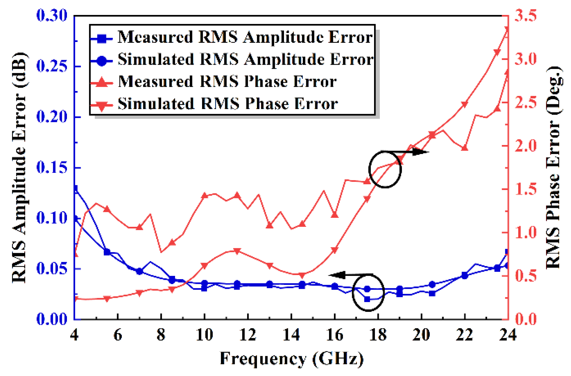
:This paper proposes a C/X/Ku/K band 6-bit digital step attenuator (DSA) which employs a variety of improved attenuation cells to achieve a wide bandwidth, stable amplitude variation, stable phase variation, and small area. In this paper, the improved T-type, π-type, and switched-path type topologies are analyzed theoretically and applied to different attenuation values to achieve the optimal attenuator performance. In addition, in order to reduce the complexity and to improve the stability of the overall radar system, the logic control circuit is integrated in the DSA chip in this paper. Finally, the proposed attenuator is implemented in 0.15μm GaAs technology, which has a maximum attenuation range of 31.5 dB with 0.5 dB steps. The proposed DSA exhibits a root-mean-square (RMS) attenuation error of less than 0.15 dB and an RMS phase error of less than 3°, at 4–24 GHz. The insertion loss (IL) and the area of the DSA are 4.3–4.5 dB and 1.5 mm × 0.4 mm, respectively. Benefiting from the improvements of the attenuation cells and the characteristic of GaAs technology with strong resistance to radiation and power processing capability, the proposed DSA is suitable for spaceborne radar systems.
1. Introduction
In modern active phased-array systems, a high beam-pointing accuracy requires effective sidelobe suppression. Therefore, a large number of power radiation distributions with sidelobe suppression have been proposed, such as the constrained least squares distribution [1], Bayliss n-bar distribution, and Taylor n-bar distribution [2]. These power radiation modes are achieved by precisely controlling the power amplitude of different array elements, which directly determine the beam formation effect of the active phased-array radar systems or multi-T/R component systems. The main amplitude control circuits are variable gain amplifiers and digital step attenuators. Variable gain amplifiers are effective devices in controlling the amplitude; however, the high-power dissipation, narrow bandwidth, and nonlinearity are the bottlenecks of their development [3,4,5]. By contrast, digital attenuators are emerging in phased array systems in virtue of their high linearity and low power dissipation [3,4,6].
Thanks to the rapid development of CMOS and SiGe BiCMOS technologies, the cost and performance of devices based on these technologies have been improved to a great extent. Recent research confirms that it is possible to achieve high-performance attenuators using CMOS technology [7,8]. However, compared with CMOS, GaAs technology indeed has certain advantages, e.g., a lower insertion loss (IL), a more stable phase error, a stronger resistance to irradiation, and a better power handling capability [9]. With the improvement and optimization of the attenuation cell, the area of the attenuator becomes smaller in GaAs technology. Therefore, GaAs technology is still preferred for spaceborne radar systems.
The conventional digital step attenuation cells are shown in Figure 1 and mainly contain distributed type [10], switched-path type [11,12], and π-type/T-type [7,8,13,14,15]. These attenuation cells have different characteristics depending on their topologies. Distributed attenuators usually have low IL because they do not have series switches; however, in this topology, the number of quarter-wavelength transmission lines increases linearly with the number of attenuation states, leading to a large chip area. Therefore, the distributed attenuators are not suitable for low-frequency applications and GaAs technology [10,16]. The switched-path attenuation cell is more suitable for large attenuation levels in broadband and precision systems. As shown in Figure 1b, this attenuation cell divides the reference and attenuation states into two separate paths capable of increasing the degree of freedom for a phase adjustment and obtaining small phase variation. However, the area and IL of this cell are larger [11,17]. π-type attenuation cells can achieve large attenuation levels and small IL, while the large phase variation of the conventional π-type attenuation cell makes it unsuitable for wideband systems [4,6]. Similarly, T-type attenuation cells also have the problem of a large phase variation in large attenuation levels, while the simple structure of the T-type makes it appropriate for small attenuation levels [7,18]. In summary, to achieve a wide bandwidth, low amplitude variation, low phase variation, and compact attenuator simultaneously, it is necessary to select reasonable attenuation cells for different attenuation levels and to provide improvements to some of the attenuation cells. Recently, some improved π-type/T-type attenuation cells with phase compensation techniques, enhancing the performance of the attenuator, have been proposed [7,8,11,12,13,14,15,16,17]. However, most of these attenuators use only one or two topologies, without rational analyses for all topologies, which cannot achieve the best performance. Therefore, there is still much room for improvement regarding the currently proposed attenuators.
In this paper, a 6-bit digital step attenuator (DSA) is designed and implemented with 0.15μm GaAs pHEMT technology. The proposed attenuator uses a variety of improved attenuation cells to achieve a wide bandwidth, high-accuracy attenuation, and small area. In summary, the main contributions of this paper are as follows.
- This paper theoretically analyzes the attenuation characteristics of various attenuation cells and their applicable attenuation levels.
- This paper simplifies the T-type attenuation cell, improves the π-type attenuation cell in two different forms, expands the switched-path attenuation cell, and provides a more reasonable cascade for these attenuation cells. These improvements enable the attenuator to achieve a more excellent performance.
- In order to reduce the complexity of the whole radar system, an on-chip logic control circuit is designed in this paper.
- Finally, this paper designs a broadband precision compact 6-bit digital attenuator with logic control circuits.
In addition, combined with the natural irradiation resistance and power handling capability of GaAs technology, the designed DSA is suitable for spaceborne radar systems. Section 2 provides an in-depth analysis and improvement of the attenuation cells with different topologies. Section 3 introduces the design of the logic control circuit. The complete attenuator circuit and experimental results are exhibited and demonstrated in Section 4. Section 5 summarizes this paper.
2. Attenuation Cells Analysis and Design
This section introduces attenuation cells with different topologies such as T-type, π-type, and switched-path type. These attenuation cells are sequentially analyzed and improved to achieve better performance.
2.1. T-Type Attenuation Cell
Figure 2 shows the schematic of the conventional switched T-type attenuation cell. The cell contains resistors and for attenuation and transistors and for state switching. In the reference state, as shown in Figure 2b, is on-state and equivalent to a small resistor that provides a path for the signal from the input to the output. Under an attenuation state, as shown in Figure 2c, is off-state and equivalent to a capacitor because of the coupling effect between the input and output, while is on-state and equivalent to a small resistor. In this state, and from the T-type network with on-state achieve the attenuation of the signal. For a required attenuation (in decibels) and characteristic impedance , the ideal values of and are given by (1) and (2).
For a conventional T-type attenuation cell with defined parameters, the transmission coefficients for the reference and attenuation states can be obtained from the transmission matrix as follows:
After replacing and in (3) and (4) with the values in (1) and (2), it can be found that the IL of the T-type attenuation cell will increase significantly and the amplitude stability will deteriorate when the T-type network is applied to a large attenuation level, as shown in Figure 3. Therefore, the T-type structure is not suitable for large attenuation levels and is used only for 0.5 dB attenuation and 1 dB attenuation in most situations.
The IL of the conventional T-type attenuation cell is related to the resistance of the series transistor in the on-state. Though increasing the gate width of the transistor can reduce the unavoidable series resistance, the large coupling capacitance generated at the same time severely degrades the phase stability of the T-type attenuation cell. Fortunately, the same function can be achieved by removing the series transistor when using the T-type structure for small attenuation cells, as shown in Figure 4. Removing the series transistor not only reduces the IL of the T-type cell but also reduces the parasitic effect, allowing the attenuation cell to achieve a wider bandwidth. As shown in Figure 5, the simplified T-type attenuation cell exhibits accurate attenuation and stable amplitude variation.
2.2. π-Type Attenuation Cell
2.2.1. Conventional π-Type Attenuation Cell
As shown in Figure 6, a conventional π-type attenuation cell consists of attenuation resistors, and , and state selection switches, and . The attenuation level is the difference in amplitude between the two states. In the reference state, is on-state and is off-state, where can be equated to a small resistor and can be equated to a capacitor, as shown in Figure 6b. Conversely, in the attenuation state, is off-state and is on-state, providing a shunt path for the signal, as shown in Figure 6c. Indeed, a good attenuator is expected to ensure that the two states have accurate attenuation amplitudes and the same phase variation over a wide frequency band. The reference and attenuation states of the conventional π-type attenuation cell are represented by Figure 6b,c, respectively, and the transmission coefficient is calculated from the transmission matrix. The calculation results are given in (5) and (6), respectively.
From (5) and (6), the insertion phase of the reference state and the attenuation state can be calculated as:
where is the characteristic impedance. For simplified calculations, and higher-order variables are omitted. As a good attenuator, the phase difference between the two states is expected to be zero.
However, in this case, it is impossible for the two states to exhibit a phase less than zero or greater than zero simultaneously; thus, the insertion phase of both states is expected to be zero to ensure that the phase difference is zero.
For a practical design, the insertion phases of both states cannot be zero, because there exists parasitic capacitance in either series or parallel branches, which leads to the generation of a non-zero phase and deteriorates the bandwidth of the attenuator. Therefore, in order to achieve broadband and accurate attenuation, two effective improvement schemes for π-type attenuators are proposed in this paper.
2.2.2. π-Type Attenuation Cell with Tail Capacitors
To solve the problem that the conventional π-type is a low-pass network in the reference state and a high-pass network in the attenuation state, an effective method is to add a tail capacitor to the shunt branch to keep the low-pass characteristic in the attenuation state. The π-type attenuation cell with tail capacitor compensation is shown in Figure 7, whose state is controlled in the same way as the conventional π-type. The reference state is where is on-state, and the attenuation state is where is off-state. When the attenuation cell is in the reference state, a low-pass path is provided by an off-capacitor of , , and a tail capacitor . Similarly, in the attenuated state, a low-pass network is also provided by the tail capacitor. The transmission coefficients for the reference and attenuation states of the improved π-type attenuation cell are calculated using the transmission matrix; such calculations are shown in (11) and (12), respectively.
The insertion phases of these two states are calculated by (11) and (12):
where and higher-order variables are omitted to simplify the calculations. Finally, the phase variation can be represented by the difference between the insertion phases of the two states:
Figure 8 shows the relative phase difference of the two states with and without the tail capacitor. It can be seen that the introduction of the tail capacitor indeed achieves the broadband phase balancing characteristic.
2.2.3. π-Type Attenuation Cell with Shunt Capacitors
The purpose of adding a tail capacitor to the shunt branch of the π-type attenuation cell is to provide a low-pass network for the attenuation state, which makes the reference and attenuation states have almost the same insertion phase. Another way to achieve a low-pass network for the attenuation state by compensating capacitors is to add shunt capacitors to the branches, as shown in Figure 9. By adding the shunt capacitors, the whole attenuation cell can be transformed into a two-pole, two-zero system. Therefore, the amplitude and phase variations can be minimized by adjusting the position of the zero and the pole in broadband. The reference and attenuation states of the π-type attenuation cell with shunt capacitance are shown in Figure 9b,c, respectively. The transmission coefficients S21 can be calculated from the transmission matrix of the two different states, as shown in (16) and (17).
The insertion phases of the two states can be easily obtained through the transmission coefficients of the two states:
where and higher-order variables are omitted to simplify the calculations. In order to obtain the minimum phase error, the phase difference between the two states is expected to be as small as possible in a wide range of bandwidth.
Figure 10 illustrates the contribution of the shunt capacitor in reducing the phase variation. It can be seen that, in the attenuation of 8 dB, the attenuation cell with shunt capacitors shows a particularly small phase change.
2.2.4. Improved π-Type Attenuation Cell Selection
It can be seen from the above discussion that both tail capacitors and shunt capacitors can provide a low-pass network to achieve the effective compensation of the attenuation cell. However, these two compensation methods are targeted to different scenarios. Adding a tail capacitor to the attenuation cell is more capable of adjusting the phase difference between the two states to zero than adding a shunt capacitor, as shown in Figure 8. However, it is worth noting that, as shown in Figure 7, when an attenuation cell with a tail capacitor performs a large attenuation level, there will be an increase in and a decrease in . In this case, there will be more signal leakage for high frequencies than low frequencies, leading to a serious amplitude instability in the wide band. On the contrary, the compensation method of adding shunt capacitors is implemented by adding a new path, which makes the amplitude variation more robust to frequency. The amplitude variation remains stable at large attenuation levels as well.
In order to achieve a better attenuator performance while taking into account amplitude flatness, bandwidth, and area, the improved π-type attenuation cell with tail capacitors is used to achieve 2 dB and 4 dB attenuation levels in this design. The improved π-type attenuator with shunt capacitors is used to achieve an 8 dB attenuation level.
2.3. Switched-Path Type Attenuation Cell
The topologies proposed above are able to achieve effective attenuation, even in small areas. However, these topologies also suffer from the same problem of not being capable of achieving large attenuation levels over a wide bandwidth. Based on the previous analysis, it can be concluded that these topologies have amplitude and phase instability at large attenuation levels. For the design of attenuation cells with large attenuation levels, some studies intend to use two identical attenuation cells for superposition [15]. For example, to achieve 16 dB attenuation, two 8 dB π-type attenuation cells are used and switched at the same state. However, this approach not only fails to demonstrate the advantages of the compactness of the T-type and π-type but also increases the complexity of the system, which creates the risk of system instability. More importantly, this approach does not reveal prominent advantages compared to the switched-path type structure. Therefore, the switched-path type structure is the better choice for large attenuation levels.
The switched-path type topology is shown in Figure 11, which divides the reference state and the attenuation state into two independent paths. In the attenuation state, is on-state and is off-state, and the signal flows from the input to the output through the upper path. In the reference state, is on-state and is off-state, and the signal flows from the input to the output through the lower path. The two independent paths allow the parasitic effects of the switches in the two paths to cancel each other out and provide a low phase error over a wide bandwidth.
In order to better regulate the phase error in the broadband, the proposed switched-path type attenuation cell uses a series inductor in the reference state and two series inductors with three resistors in the attenuation state, as shown in Figure 11. This structure provides more freedom for the phase regulation of the attenuation cell, making it easier to achieve phase balance. In addition, this topology is desired to ensure two entirely independent paths, i.e., one path should be completely cut off while the other path is working. Therefore, the off-isolation of the two paths seems particularly important. In the design of this paper, two leakage switches, and , are added to the reference and attenuation paths of the switched-path attenuation cell, respectively, as shown in Figure 11. To ensure that the signal can be effectively leaked when the path is cut off, and are in opposite states to and , respectively. In this way, it is possible to ensure that the signal passes through only one path, making the phase variation smaller and achieving a broadband balance of phases. The phase variation between the reference state and the attenuation state of the switched-path attenuation cell is shown in Figure 12, which shows that the two paths both have similar phase variations and a small relative phase.
2.4. Cascade of Attenuation Cells
The design of the attenuator should ensure that each attenuation cell has an accurate attenuation level, a small phase variation, and a wide bandwidth. The performance of each cell will eventually affect the root-mean-square (RMS) attenuation error, bandwidth, etc. of the whole attenuator. The 6-bit DSA designed in this paper is shown in Figure 13, which contains two T-type cells, two π-type cells with tail capacitor compensation, one π-type cell with shunt capacitor compensation, and one switched-path cell, achieving 0.5 dB, 1 dB, 2 dB, 4 dB, 8 dB, and 16 dB attenuation, respectively. The 16 dB cell is placed in the middle because this cell uses a switched-path topology and has better isolation. The 2 dB and 4 dB cells have smaller attenuation levels with the improved π-type cells, so they have better s-parameters and are placed at both ends. Using such a cascade sequence of attenuation cells can improve the performance of the overall attenuator. Meanwhile, a large series gate resistor is used to reduce the leakage of radio frequency (RF) signals and weaken the coupling effect of the parasitic capacitor.
3. Logic Control Circuits
The attenuators are often integrated in T/R modules, which have single-ended (positive) control voltages to make them uncomplicated, compact, and low-cost. However, most designs of GaAs-based microwave devices use GaAs pHEMT based on the negative bias voltage. Therefore, in order to improve the overall system performance, it is necessary to design logic control circuits to transfer the positive voltage to the negative voltage. In this paper, an on-chip integrated direct-coupled FET logic (DCFL) control circuit is designed due to the low DC consumption, small chip area, and fast response [19,20], which is capable of converting 0/+5 voltages to −5/0 voltages.
The designed logic control circuit is shown in Figure 14, which consists of E-mode pHEMT and D-mode pHEMT. The E-mode pHEMT determines the threshold value of the inverter, and the D-mode pHEMT acts as the load for the control circuit. The final output voltage is −5 or 0 V. In this figure, and are two complementary voltages. The results of the time domain transient simulation in the case of the input pulse voltage being 5 V are shown in Figure 15.
4. Simulation and Measurement Results
The proposed 6-bit DSA has been fabricated in the 0.15 μm GaAs pHEMT technology, which is a mature technology and has high-yield, low-noise, and low-cost characteristics. The chip micrograph is shown in Figure 16. The core area of the attenuator is 0.4 mm × 1.5 mm, and the attenuator is measured on-wafer by using a Cascade Summit 1200 M probe station and a Keysight N5245A microwave network analyzer. In Figure 17, the simulated and measured attenuation results of the major states are demonstrated. Although the measured results exhibit larger IL due to the additional interconnect structure, they still show a stable attenuation in 4–24 GHz. The simulated and measured relative phase variations for major states are given in Figure 18, where the measured results are quite similar to the simulated results. It can be seen that the designed attenuation cells all show satisfactory performance. The measured results for and are shown in Figure 19a,b, respectively. Thanks to good matching and cascade optimization, the input and output reflection coefficients of all attenuation states are below −18 dB, which will increase the overall stability of the system and reduce the IL of the attenuator. Figure 20 exhibits the measured results of all attenuation states. The simulated and measured amplitude error RMS and relative phase error RMS are given in Figure 21. The amplitude error RMS is less than 0.15 dB and the relative phase RMS is less than 3° over the entire operating band, which demonstrates great performance for processing. Table 1 summarizes the performance of the proposed attenuator and compares it with the relevant state-of-the-art literature. In this table, the III–V technology exhibits significant advantages in terms of insertion loss and relative phase variation compared to silicon technology. More importantly, the attenuator designed in this paper based on the III–V technology achieves a similar area with the silicon technology, which demonstrates the high compactness of the proposed design. Compared with other attenuators based on III–V technologies, the proposed attenuator exhibits superior performance in many aspects due to the reasonable selection, improvement, and cascading of attenuation cells.
5. Conclusions
This paper proposes a broadband precision 6-bit DSA with 0.15 μm GaAs pHEMT technology. Compared with silicon technology, GaAs technology exhibits stronger advantages in irradiation resistance and power handling capability. In our design, the characteristics of various attenuation cells are analyzed theoretically, and suitable attenuation cells are selected for different attenuation levels. In order to enhance the performance of the designed attenuator, the selected attenuation cells are improved in various ways. These improved attenuation cells are further optimized for cascading. As a result, a high-performance and compact attenuator with III-V technology is achieved, which has an amplitude error RMS below 0.15 dB, a phase error RMS below 3°, and and below −18 dB in 4–24 GHz. At the same time, the on-chip logic control circuit is designed in this paper, which greatly reduces the overall complexity and improves the stability of the radar system. Unfortunately, the designed attenuator has a larger area compared to the attenuators with silicon technology, though it has a relatively small area with III-V technology. The designed attenuator has overlapped states below 1 GHz, which need to be improved in our future research. Overall, the designed attenuator has the merits of accurate and stable attenuation levels, a wide bandwidth, a strong irradiation resistance, and power handling capability. Therefore, the designed attenuator is suitable for future broadband radar systems which concentrate on multi-function, multiple operating modes, and MIMO.
Author Contributions
Conceptualization, J.Z.; methodology, J.Z.; software, J.Z.; validation, J.Z., J.L. and Y.Y.; formal analysis, J.Z. and Z.Y.; investigation, J.Z.; resources, J.Z.; data curation, J.Z. and Y.Y.; writing—original draft preparation, J.Z. and Y.Y.; writing—review and editing, J.Z.; visualization, J.Z.; supervision, J.Z., C.T. and Z.Y.; project administration, J.Z. and Z.Y.; funding acquisition, Z.Y. All authors have read and agreed to the published version of the manuscript.
Funding
This work was supported in part by the National Natural Science Foundation of China (61971026).
Institutional Review Board Statement
Not applicable.
Informed Consent Statement
Not applicable.
Data Availability Statement
The data that support the findings of this study are available from the corresponding author upon reasonable request.
Conflicts of Interest
The authors declare no conflict of interest.
References
- Melde, K.L.; Taylor, M.L. Pattern characteristics of linear arrays using the constrained least squares distribution. IEEE Trans. Antennas Propag. 2003, 51, 772–775. [Google Scholar] [CrossRef]
- Zinka, S.R.; Kim, J.P. On the Generalization of Taylor and Bayliss n-bar Array Distributions. IEEE Trans. Antennas Propag. 2012, 60, 1152–1157. [Google Scholar] [CrossRef]
- Dogan, H.; Meyer, R.G. Intermodulation Distortion in CMOS Attenuators and Switches. IEEE J. Solid-State Circuits 2007, 42, 529–539. [Google Scholar] [CrossRef]
- Dogan, H.; Meyer, R.G.; Niknejad, A.M. Analysis and Design of RF CMOS Attenuators. IEEE J. Solid-State Circuits 2008, 43, 2269–2283. [Google Scholar] [CrossRef]
- Koutani, M.; Kawamura, H.; Toyoyama, S.; Iizuka, K. A Digitally Controlled Variable-gain Low-noise Amplifier with Strong Immunity to Interferers. In Proceedings of the 2006 IEEE Asian Solid-State Circuits Conference, Hangzhou, China, 13 November 2006; pp. 71–74. [Google Scholar] [CrossRef]
- Huang, Y.-Y.; Woo, W.; Yoon, Y.; Lee, C.-H. Highly Linear RF CMOS Variable Attenuators With Adaptive Body Biasing. IEEE J. Solid-State Circuits 2011, 46, 1023–1033. [Google Scholar] [CrossRef]
- Song, I.; Cho, M.-K.; Cressler, J.D. Design and Analysis of a Low Loss, Wideband Digital Step Attenuator With Minimized Amplitude and Phase Variations. IEEE J. Solid-State Circuits 2018, 53, 2202–2213. [Google Scholar] [CrossRef]
- Zhao, C.; Zeng, X.; Zhang, L.; Liu, H.; Yu, Y.; Wu, Y.; Kang, K. A 37–40-GHz Low-Phase-Imbalance CMOS Attenuator With Tail-Capacitor Compensation Technique. IEEE Trans. Circ. Syst. I Regul. Pap. 2020, 67, 3400–3409. [Google Scholar] [CrossRef]
- Doddamani, N.D.; Harishchandra; Nandi, A.V. Design of SPDT Switch, 6 Bit Digital Attenuator, 6 Bit Digital Phase Shifter for L-Band T/R Module using 0.7 μM GaAs MMIC Technology. In Proceedings of the 2007 International Conference on Signal Processing, Communications and Networking, Chennai, India, 22 February 2007; pp. 302–307. [Google Scholar] [CrossRef]
- Min, B.-W.; Rebeiz, G.M. A 10–50-GHz CMOS Distributed Step Attenuator With Low Loss and Low Phase Imbalance. IEEE J. Solid-State Circuits 2007, 42, 2547–2554. [Google Scholar] [CrossRef]
- Sjogren, L.; Ingram, D.; Biedenbender, M.; Lai, R.; Allen, B.; Hubbard, K. A low phase-error 44-GHz HEMT attenuator. IEEE Microw. Guided Wave Let. 1998, 8, 194–195. [Google Scholar] [CrossRef]
- Kim, J.-G.; Lee, K.-H. An S/C/X-Band 4-Bit Digital Step Attenuator MMIC with 0.25 μm GaN HEMT Technology. Appl. Sci. 2022, 12, 4717. [Google Scholar] [CrossRef]
- Zhao, C.; Guo, J.; Liu, H.; Yu, Y.; Wu, Y.; Kang, K. A 33–41-GHz SiGe-BiCMOS Digital Step Attenuator With Minimized Unit Impedance Variation. IEEE Trans. Very Large Scale Integ. (VLSI) Syst. 2021, 29, 568–579. [Google Scholar] [CrossRef]
- Cheon, C.D.; Rao, S.G.; Lim, W.; Cardoso, A.S.; Cho, M.-K.; Cressler, J.D. Design Methodology for a Wideband, Low Insertion Loss, Digital Step Attenuator in SiGe BiCMOS Technology. IEEE Trans. Circuits Syst. II Exp. Briefs 2022, 69, 744–748. [Google Scholar] [CrossRef]
- Li, N.; Zhang, Z.; Li, M.; Gao, H.; Wang, S.; Song, C.; Xu, Z. A DC–28-GHz 7-Bit High-Accuracy Digital-Step Attenuator in 55-nm CMOS. IEEE Microw. Wireless Compon. Lett. 2022, 32, 157–160. [Google Scholar] [CrossRef]
- Kim, K.; Lee, H.-S.; Min, B.-W. V-W Band CMOS Distributed Step Attenuator With low Phase Imbalance. IEEE Microw. Wireless Compon. Lett. 2014, 24, 548–550. [Google Scholar] [CrossRef]
- Cho, M.-K.; Kim, J.-G.; Baek, D. A Broadband Digital Step Attenuator with Low Phase Error and Low Insertion Loss in 0.18-μm SOI CMOS Technology. Electron. Telecommun. Res. Inst. J. 2013, 35, 638–643. [Google Scholar]
- Cheng, W.; Alink, M.S.O.; Annema, A.J.; Wienk, G.J.M.; Nauta, B. A Wideband IM3 Cancellation Technique for CMOS π and T-Attenuators. IEEE J. Solid-State Circuits 2013, 48, 358–368. [Google Scholar] [CrossRef]
- Luo, W.; Liu, H.; Zhang, Z.; Sun, P.; Liu, X. High-Power X-Band 5-b GaN Phase Shifter With Monolithic Integrated E/D HEMTs Control Logic. IEEE Trans. Elect. Dev. 2017, 64, 3627–3633. [Google Scholar] [CrossRef]
- Hao, D.; Zhang, W.; Liu, X.; Liu, Y. A Wideband 6-Bit Digital Attenuator in a GaAs pHEMT MMIC. Electronics 2022, 11, 2166. [Google Scholar] [CrossRef]
- Khabbaz, B.; Pospishil, A.; Singh, H.P. DC-to-20-GHz MMIC multibit digital attenuators with on-chip TTL control. IEEE J. Solid-State Circuits 1992, 27, 1457–1462. [Google Scholar] [CrossRef]
- Longhi, P.E.; Colangeli, S.; Ciccognani, W.; Limiti, E. Improved microwave attenuator topology minimizing the number of control voltages. Microw. Opt. Technol. Lett. 2019, 61, 926–929. [Google Scholar] [CrossRef]
- Wang, K.; Zhou, T.; Zhang, H.; Qiu, L. A 28–40-GHz Digital Step Attenuator With Low Amplitude and Phase Variations. IEEE Microw. Guided Wave Lett. 2021, 31, 64–67. [Google Scholar] [CrossRef]
Figure 1.
Topology of digital step attenuation cells. (a) Distributed step attenuator. (b) Switched-path attenuator. (c) T-type attenuation cell. (d) π-type attenuation cell.
Figure 1.
Topology of digital step attenuation cells. (a) Distributed step attenuator. (b) Switched-path attenuator. (c) T-type attenuation cell. (d) π-type attenuation cell.
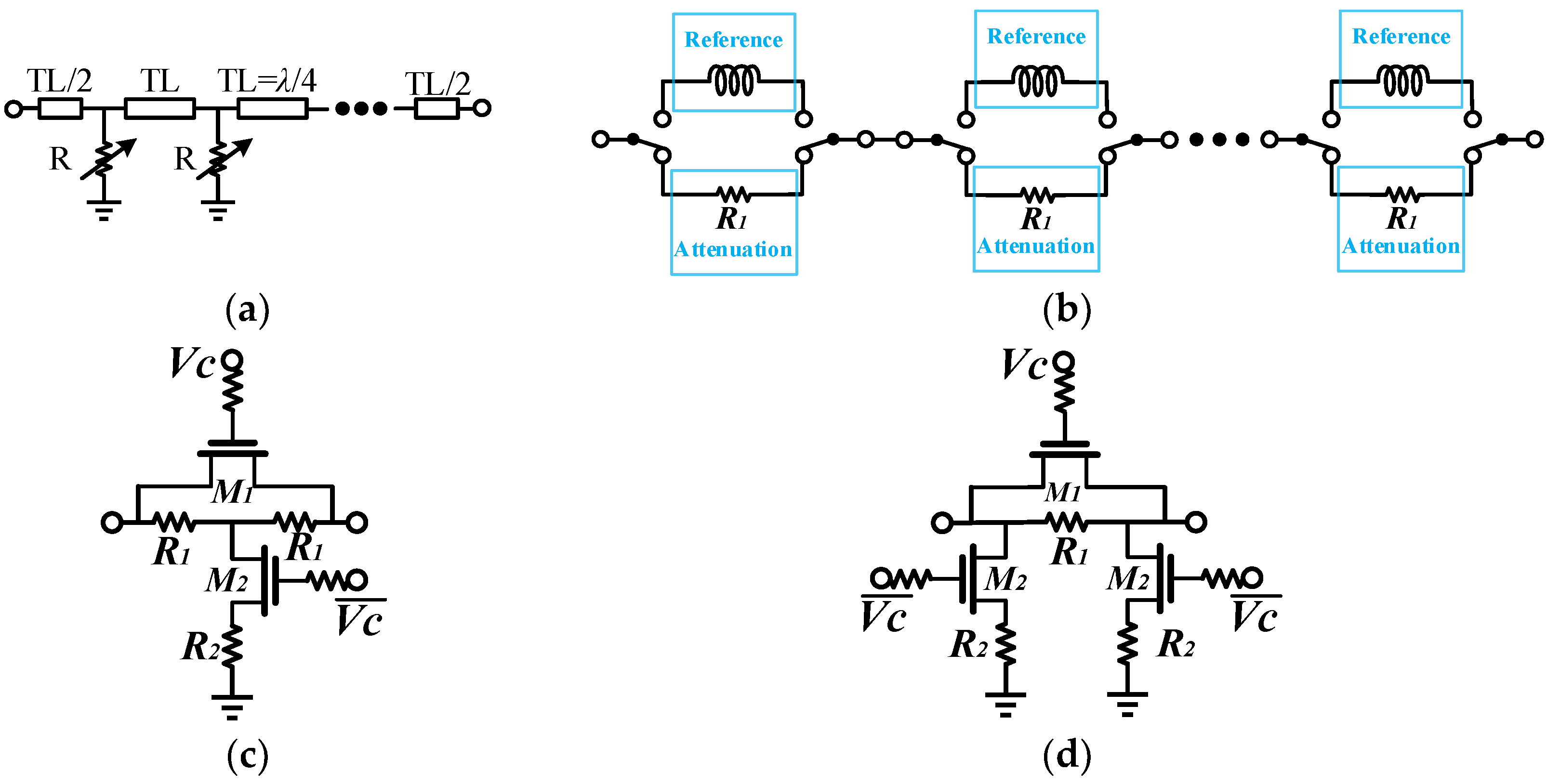
Figure 2.
(a) The schematic of the conventional switched T-type attenuation cell. (b) Reference state. (c) Attenuation state.
Figure 2.
(a) The schematic of the conventional switched T-type attenuation cell. (b) Reference state. (c) Attenuation state.
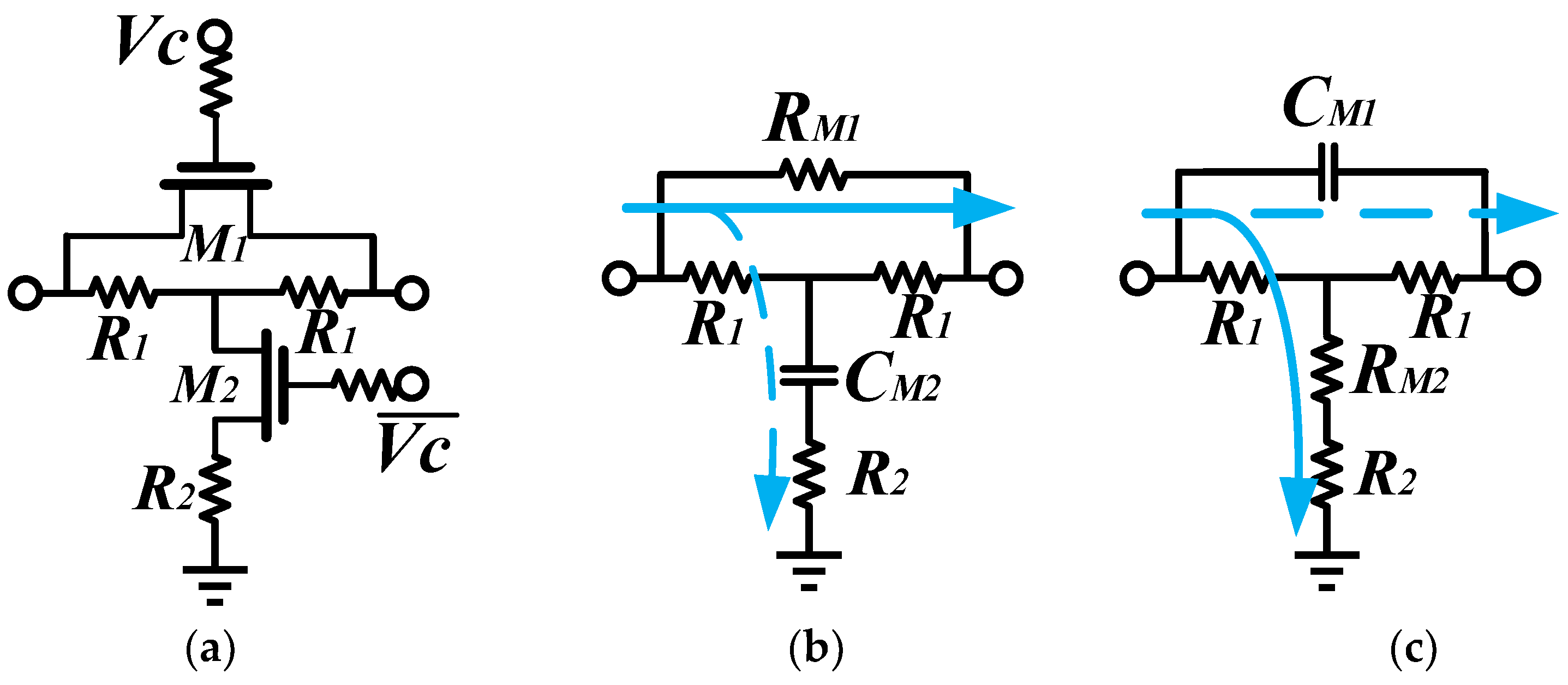
Figure 3.
The relative attenuation of the conventional T-type attenuation cell.
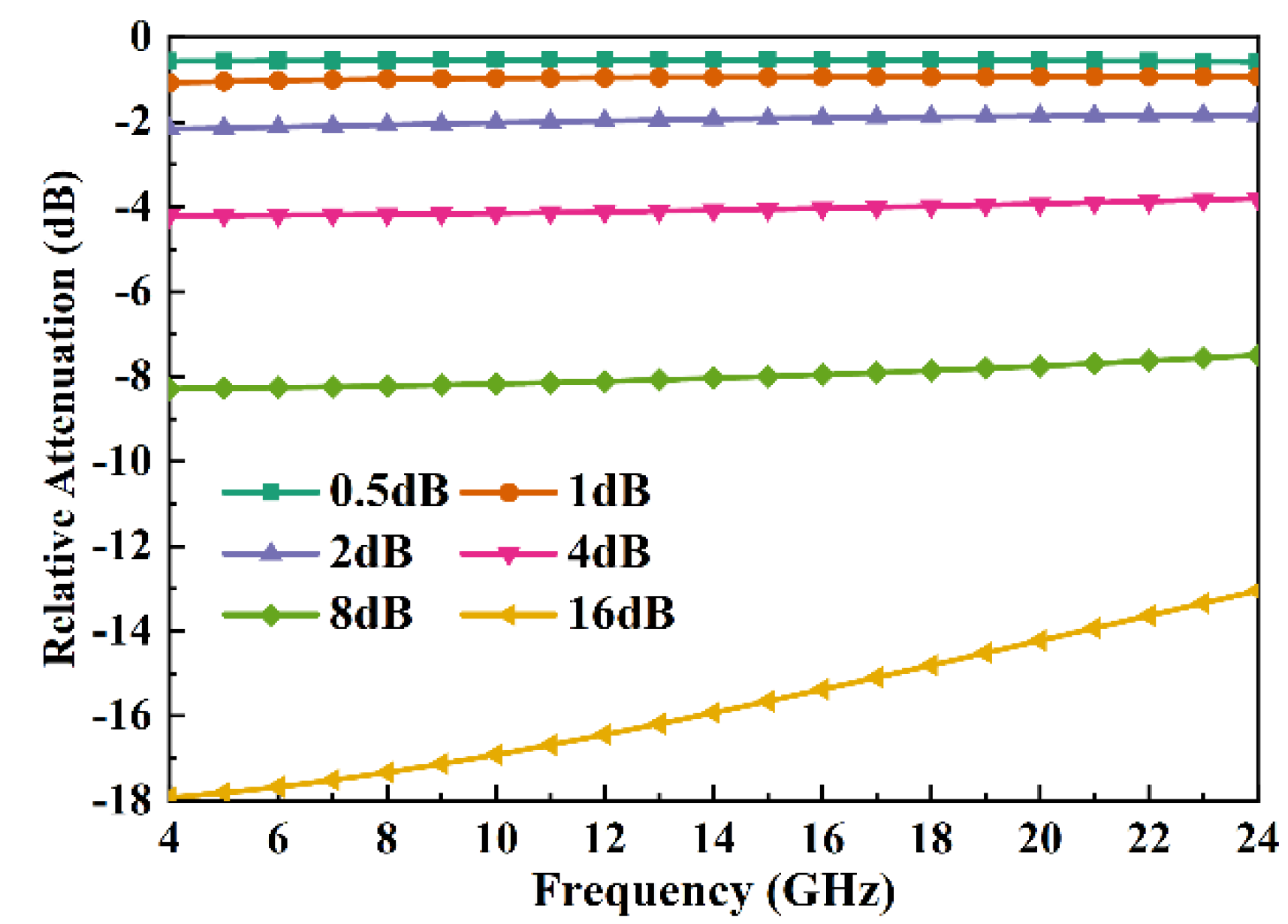
Figure 4.
The schematic of the (a) conventional T-type attenuation cell and (b) simplified T-type attenuation cell.
Figure 4.
The schematic of the (a) conventional T-type attenuation cell and (b) simplified T-type attenuation cell.
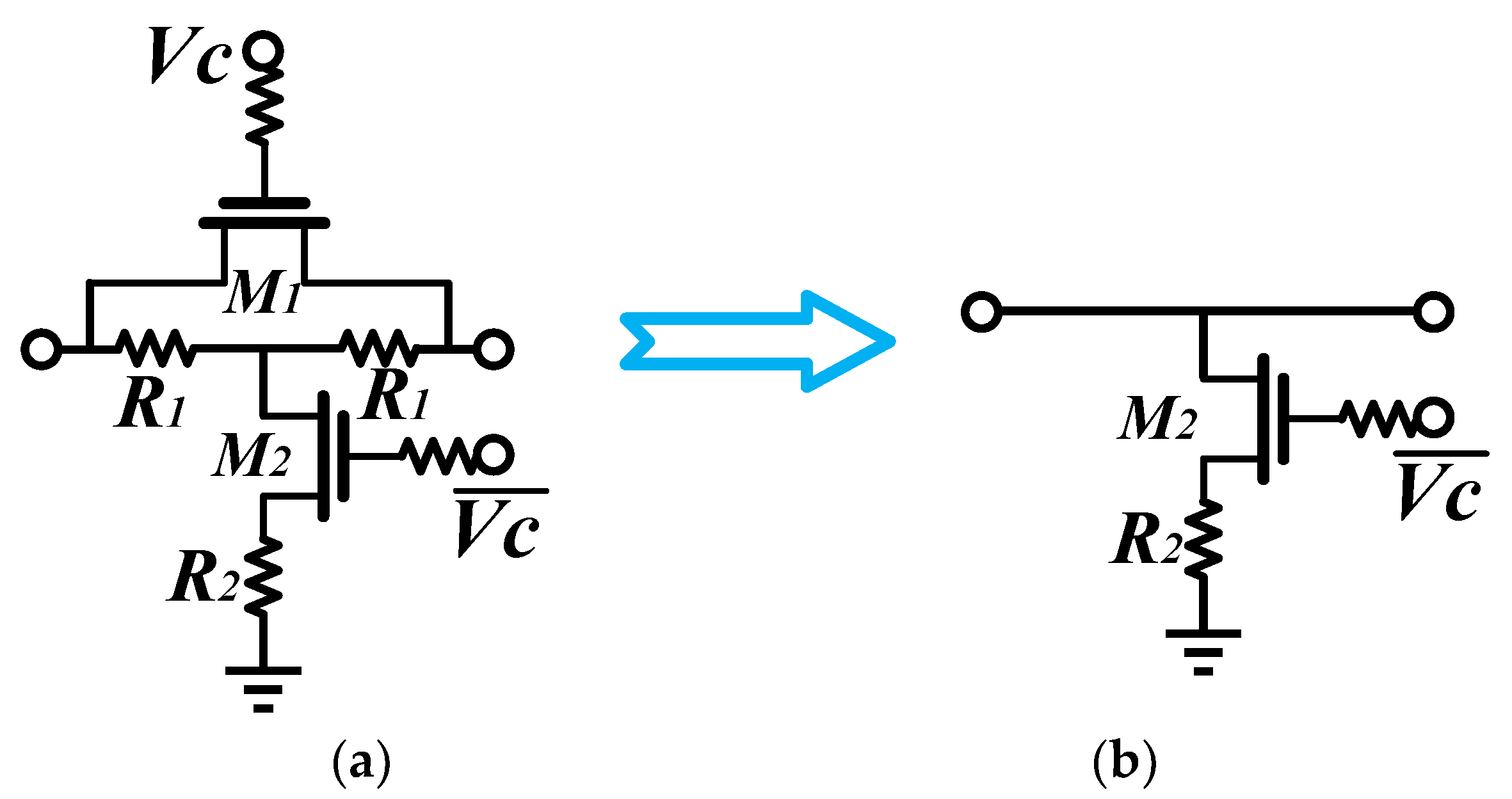
Figure 5.
Comparison of the relative attenuation between the conventional and simplified T-type attenuation cell.
Figure 5.
Comparison of the relative attenuation between the conventional and simplified T-type attenuation cell.

Figure 6.
(a) The schematic of the conventional switched π-type attenuation cell. (b) Reference state. (c) Attenuation state.
Figure 6.
(a) The schematic of the conventional switched π-type attenuation cell. (b) Reference state. (c) Attenuation state.
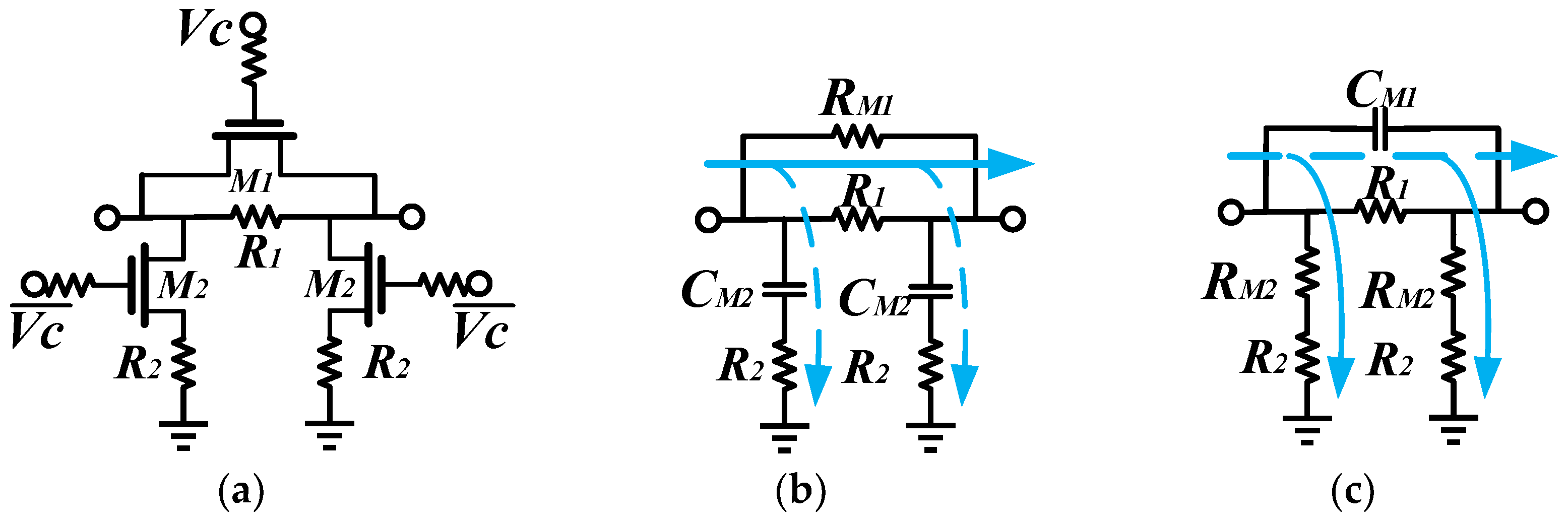
Figure 7.
(a) The schematic of the switched π-type attenuation cell with tail capacitors. (b) Reference state. (c) Attenuation state.
Figure 7.
(a) The schematic of the switched π-type attenuation cell with tail capacitors. (b) Reference state. (c) Attenuation state.
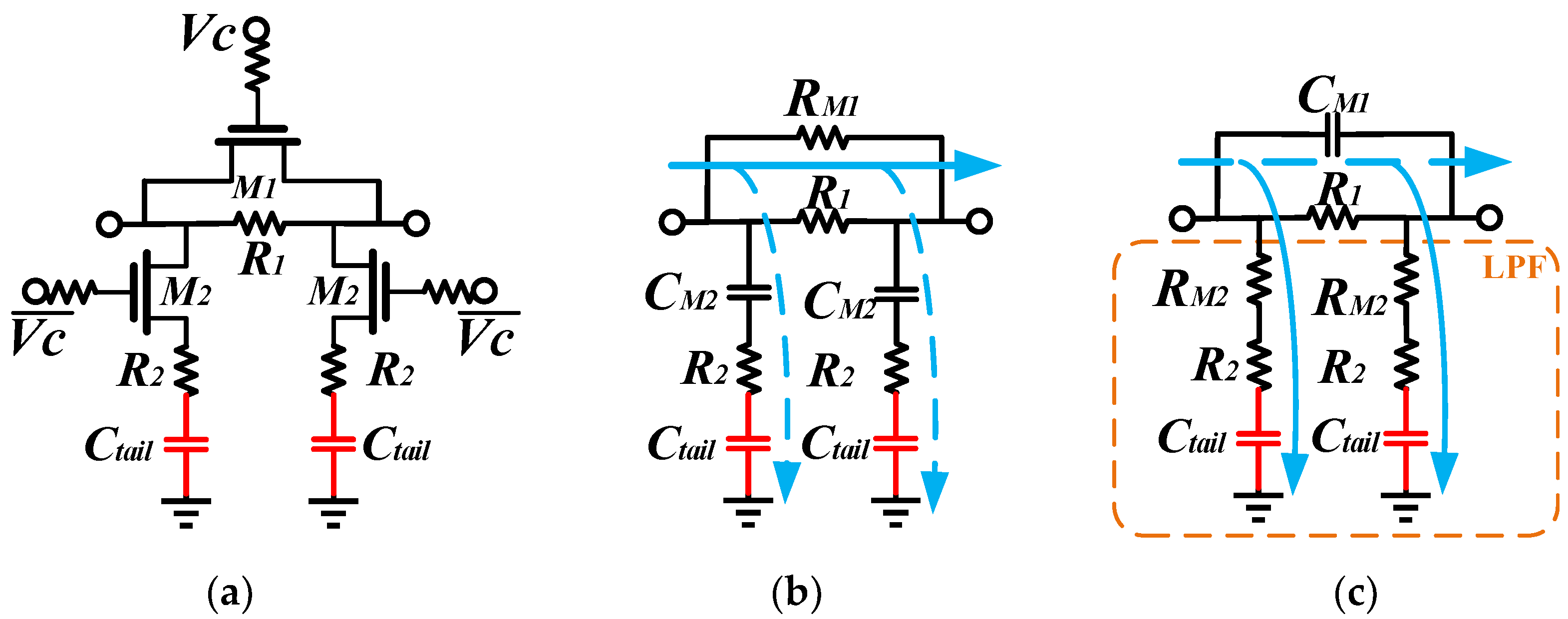
Figure 8.
Comparison of the relative phase variation between the conventional and improved π-type attenuation.
Figure 8.
Comparison of the relative phase variation between the conventional and improved π-type attenuation.

Figure 9.
(a) The schematic of the switched π-type attenuation cell with shunt capacitors. (b) Reference state. (c) Attenuation state.
Figure 9.
(a) The schematic of the switched π-type attenuation cell with shunt capacitors. (b) Reference state. (c) Attenuation state.
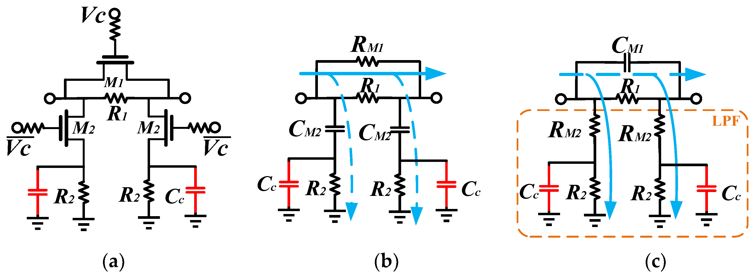
Figure 10.
Comparison of the relative phase variation between the conventional attenuation and both of the improved π-type attenuations.
Figure 10.
Comparison of the relative phase variation between the conventional attenuation and both of the improved π-type attenuations.

Figure 11.
The schematic of the switched-path attenuation cell.

Figure 12.
The phase variation between the reference state and the attenuation state of the switched−path attenuation cell.
Figure 12.
The phase variation between the reference state and the attenuation state of the switched−path attenuation cell.

Figure 13.
The simplified schematic of the proposed 6-bit DSA.
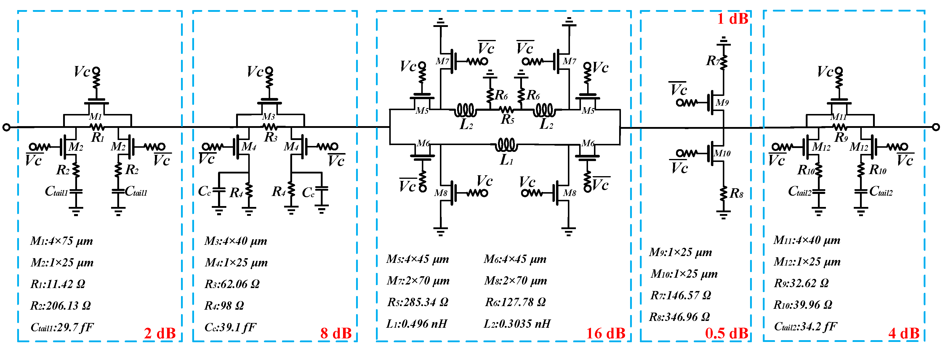
Figure 14.
The schematic of the designed logic control circuit.
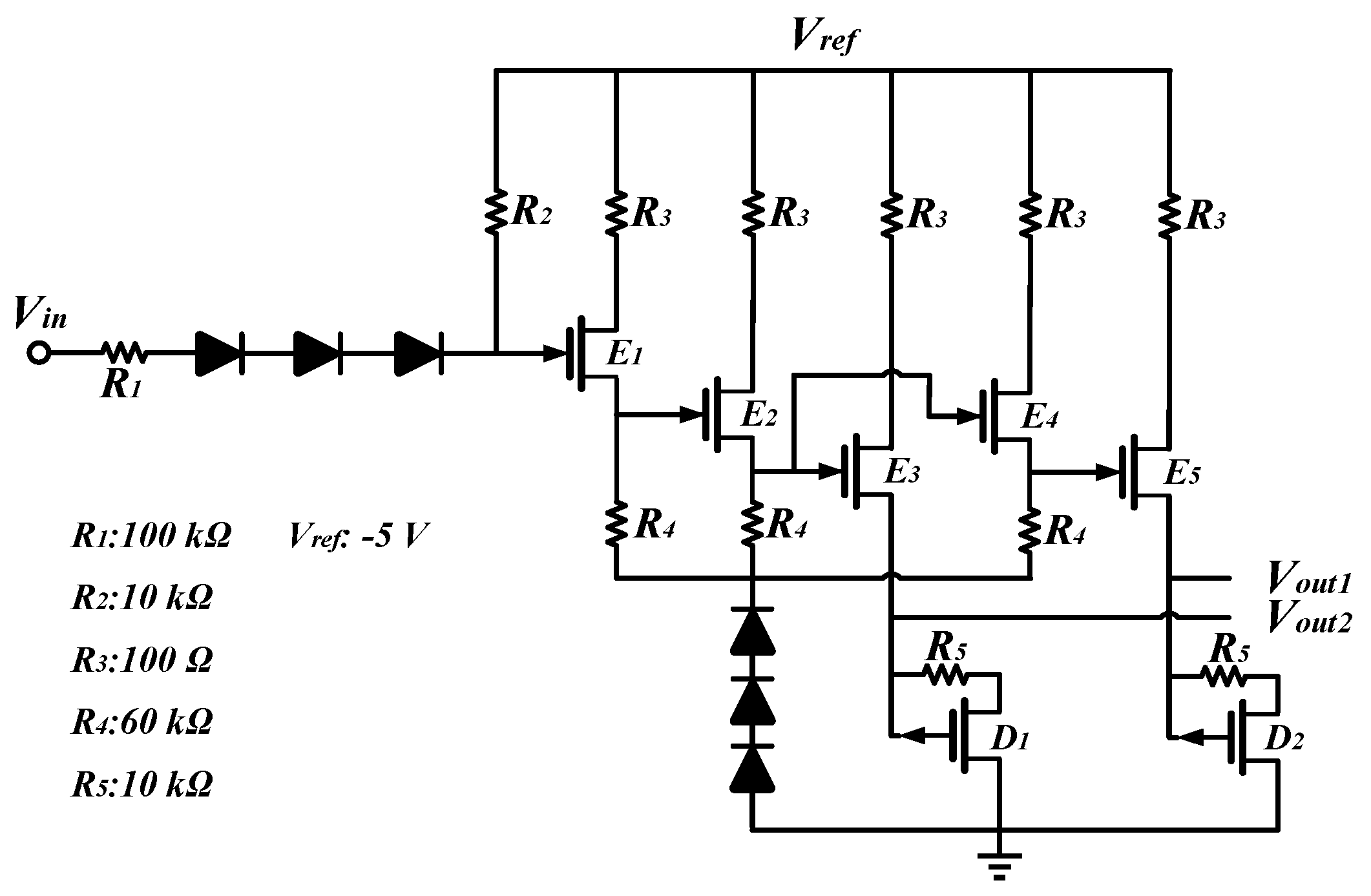
Figure 15.
The time domain transient simulation results of the logic control circuit.

Figure 16.
Micrograph of the proposed 6-bit DSA.

Figure 17.
The simulated and measured attenuation results of the major states.
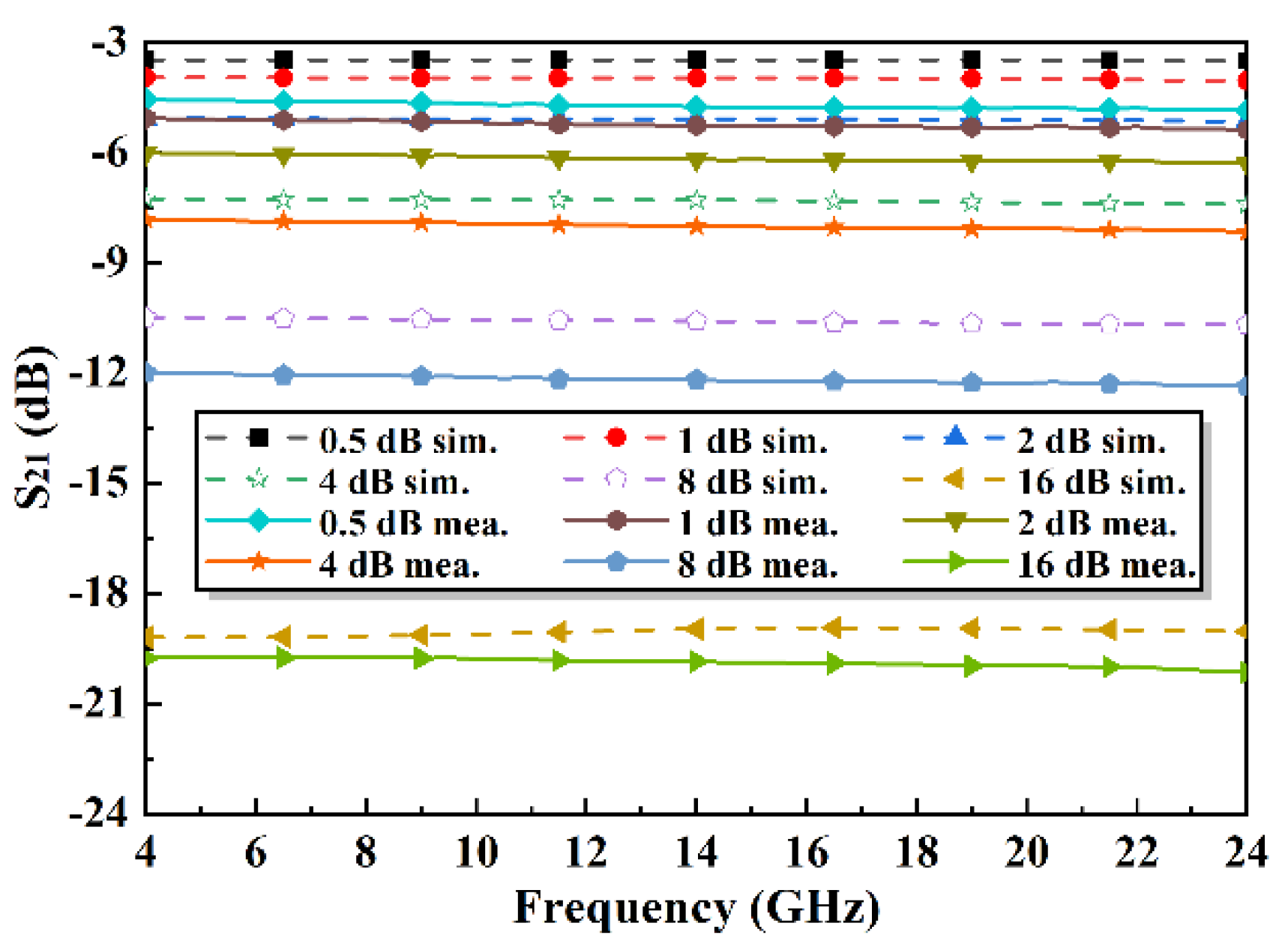
Figure 18.
The simulated and measured relative phase variations for the major states.
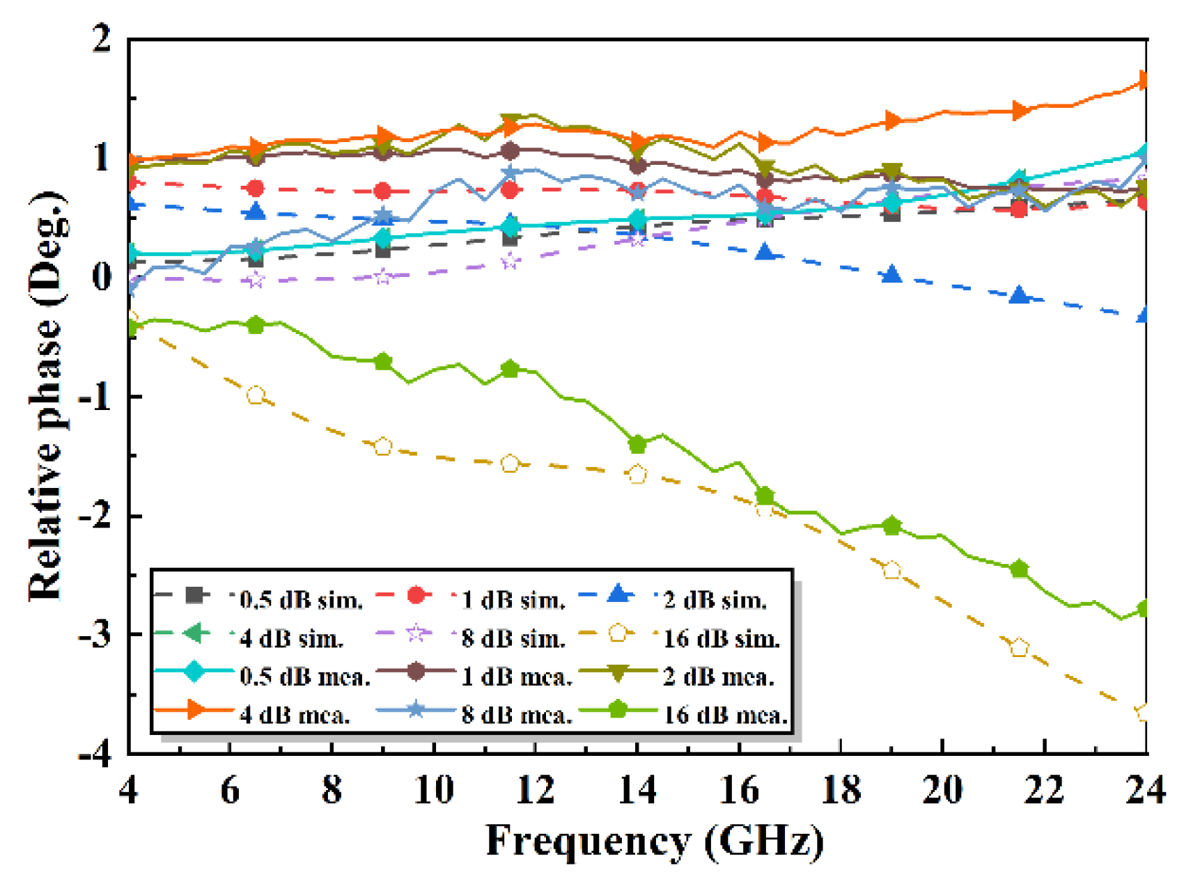
Figure 19.
The measured (a) and (b) of all states.
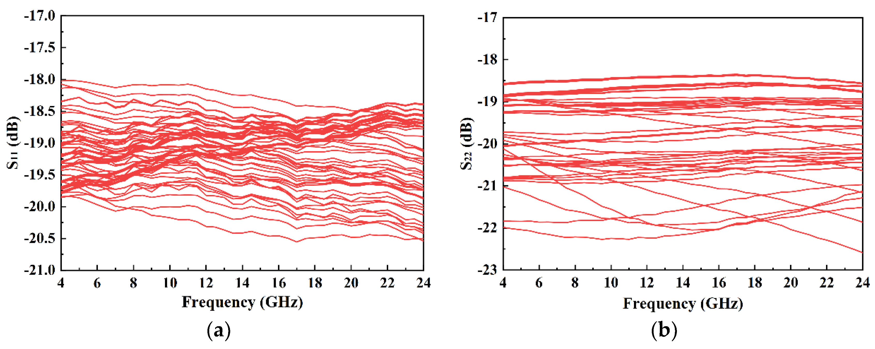
Figure 20.
The measured relative attenuation of all states.
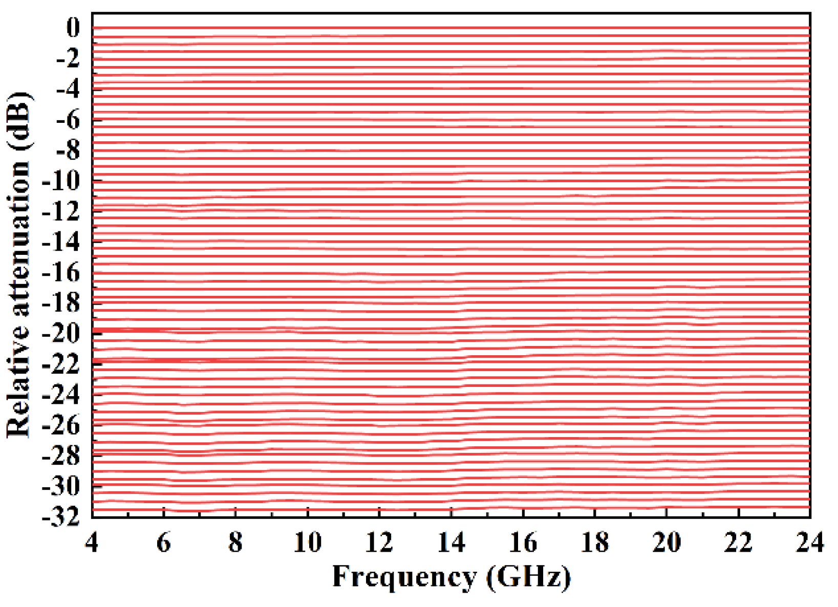
Figure 21.
The simulated and measured amplitude error RMS and relative phase error RMS.

Table 1.
Performance comparison with state-of-the-art DSAs.
| Reference | [21] | [22] | [4] | [8] | [7] | [13] | [23] | This Work |
|---|---|---|---|---|---|---|---|---|
| Technology | GaAs FET | GaAs | 0.13 μm CMOS | 65 nm CMOS | 0.13 μm SiGe BiCMOS | 0.13 μm SiGe BiCMOS | 0.13 μm SiGe BiCMOS | 0.15 μm GaAs PHEMT |
| Topology | Distributed T-type | T-type | T-type | T-type π-type | T-type | T-type π-type | π-type | T-type π-type Switched-path |
| Bandwidth (GHz) | DC-20 | 4–8 | 0–2.5 | 37–40 | DC-20 | 33–41 | 28–40 | 4–24 |
| Step (dB)/Bit | 1.5/4 | 0.5/5 | / | 1/5 | 0.5/6 | 0.5/5 | 1/5 | 0.5/6 |
| Attenuator Range (dB) | 22.5 | 15.5 | 42 | 31.5 | 31.5 | 15.5 | 31 | 31.5 |
| IL (dB) | 3.1–4.8 | 4.8 | 0.9–3.5 | 7 | 4 | 13 | 5.4–9.1 | 4.2–4.5 |
| Return Loss (dB) | >13 | / | >8.2 | >12 | >10 | >10 | >10 | >18 |
| RMS Attenuation (dB) | 0.5 | 0.2 | / | 0.27 | 0.37 | 0.2 | 0.43 | 0.15 |
| RMS Phase (Deg.) | / | / | / | 3.7 | 4 | 2.5 | 5.4 | 3 |
| Size (mm) | 2.6 × 1.6 | 1.8 × 1.2 | / | 0.51 × 0.42 | 1 × 0.14 | 0.5 × 0.44 | (0.21 mm2) | 1.5 × 0.4 |
Publisher’s Note: MDPI stays neutral with regard to jurisdictional claims in published maps and institutional affiliations. |
© 2022 by the authors. Licensee MDPI, Basel, Switzerland. This article is an open access article distributed under the terms and conditions of the Creative Commons Attribution (CC BY) license (https://creativecommons.org/licenses/by/4.0/).
Share and Cite
MDPI and ACS Style
Zeng, J.; Li, J.; Yuan, Y.; Tan, C.; Yu, Z. A C/X/Ku/K-Band Precision Compact 6-Bit Digital Attenuator with Logic Control Circuits. Electronics 2022, 11, 3620. https://doi.org/10.3390/electronics11213620
AMA Style
Zeng J, Li J, Yuan Y, Tan C, Yu Z. A C/X/Ku/K-Band Precision Compact 6-Bit Digital Attenuator with Logic Control Circuits. Electronics. 2022; 11(21):3620. https://doi.org/10.3390/electronics11213620
Chicago/Turabian StyleZeng, Jialong, Jiaxuan Li, Yang Yuan, Cheng Tan, and Zhongjun Yu. 2022. "A C/X/Ku/K-Band Precision Compact 6-Bit Digital Attenuator with Logic Control Circuits" Electronics 11, no. 21: 3620. https://doi.org/10.3390/electronics11213620
Note that from the first issue of 2016, this journal uses article numbers instead of page numbers. See further details here.