
Analysis of HBM Failure in 3D NAND Flash Memory
by
Biruo Song
1,2,3, 
Zhiguo Li
3,
Xin Wang
3,
Xiang Fu
3,
Fei Liu
1,
Lei Jin
1,2,3 and
Zongliang Huo
1,2,3,* 1
Institute of Microelectronics of the Chinese Academy of Sciences, Beijing 100029, China
2
University of Chinese Academy of Sciences, Beijing 100049, China
3
Yangtze Memory Technologies Co., Ltd., Wuhan 430205, China
*
Author to whom correspondence should be addressed.
Electronics 2022, 11(6), 944; https://doi.org/10.3390/electronics11060944
Submission received: 10 January 2022
/
Revised: 4 March 2022
/
Accepted: 9 March 2022
/
Published: 18 March 2022
(This article belongs to the Section Microelectronics)
Abstract
:Electrostatic discharge (ESD) events are the main factors impacting the reliability of NAND Flash memory. The behavior of human body model (HBM) failure and the corresponding physical mechanism of 3D NAND Flash memory are investigated in this paper. A catastrophic burn-out failure during HBM zapping is first presented. Analysis shows that NMOS fingers’ local heating induced by inhomogeneous substrate resistance Rsub and local heating induced by the drain contact and 3D stacked IC (SIC) structure lead to the failure. Therefore, a new approach is proposed to reduce local heat generation. Finally, by increasing N+ length (NPL) and introducing a novel contact strip, the silicon result shows enhanced ESD robustness.
1. Introduction
ESD testing is one of the major reliability qualifications for NAND Flash memory [1]. A common ESD event referred to as the human body model (HBM) is widely used to characterize device reliability when the charge in the human body is being transferred to the ground through integrated circuits. In addition, transmission line pulse (TLP) testing can provide reference for critical parameters in the ESD circuit [2,3,4]. Thus, testing with a combination of HBM and TLP is common practice [5,6]. There are some other efficient techniques that can be used for ESD robustness, such as TCAD simulation, layout modeling, and ESD device modeling [7,8,9,10,11,12,13,14,15,16], which enable quick pinpointing of design weakness and reduced development cycle and costs.
Nowadays, NAND Flash memory is widely used in mass storage applications. Three-dimensional NAND Flash memory with 3D stacked IC (SIC) [17,18] is the most viable solution for high-capacity storage and low-bit-cost non-volatile memory [19,20]. During the contact-type usage, the pins of packaged die may be exposed to ESD sources such as human fingers; hence, ESD immunity is required for NAND Flash memory. Thus, the study of ESD damage on 3D NAND Flash memory is of great significance.
In this paper, a severe HBM burn-out failure in 3D NAND Flash ESD stress is investigated. Local heating induced by inhomogeneous Rsub, the drain contact, and the 3D SIC structure is verified to be the cause of the ESD clamp failure. Consequently, an improvement in heat generation is proposed. Silicon analysis demonstrates the validity of process refinement.
2. ESD Clamp Device Structure
A simplified cross-sectional view of a 3D NAND Flash test chip is shown in Figure 1. Two stacking wafers are connected together by millions of bonding interface vias (BIVs) [17,18]. As shown in the figure, the ESD pad on the backside of the upper wafer is connected to the ESD clamp circuit on the lower wafer through BIVs in between the two wafers [21,22,23,24]. During the ESD test, test voltage is applied to the metal pad on the top and discharge through the ESD clamp at the bottom.
The NMOS transistors used in the ESD clamp were fabricated with NAND technology. Figure 2 illustrates the cross-section and equivalent circuit of the HV NMOS of the ESD protection circuit in the NAND Flash test chip. N+ diffusion of the drain/source side is located inside the N-type lightly doped drain (N-LDD) area. Under the drain and source contacts (CTs), there is the silicide layer. The length from the drain contact to the N+ edge and the length from the N+ edge to the gate poly are referred to as N+ length (NPL) and N-LDD length (NLL), respectively.
The simplified layout top view of the multi-finger NMOS in the ESD clamp is illustrated in Figure 3, with eight fingers shown. The multiple NMOS fingers are surrounded by a P+ guard ring, with their gate, source, and drain connected in parallel. The ground pad VSS is located at the right side of the floorplan and is outside of the P+ guard ring.
3. HBM Testing System
In order to evaluate the ESD robustness of the NAND Flash test chip, an HBM test was performed on packaged dies. A KeyTek MK2 ESD tester was used. The HBM stress model is shown in Figure 4. The tester can provide a stepped testing voltage of up to 8 KV.
4. Experimental Results and Discussion
4.1. HBM Test Results
The general specification of a NAND Flash memory HBM test is 2 KV [25,26]. The testing voltage for HBM testing starts from 250 V and increases by 250 V per step. In this paper, an HBM test was performed on both a raw test chip sample and an optimized test chip sample with process splits. Failures were observed during the HBM test on the raw test chip sample. The process splits were then processed and verified through an HBM test.
Three raw test chip samples were chosen for the HBM test. As shown in Table 1, they failed at 1 KV, 1.25 KV and 1.5 KV. For each failed sample, the test voltage presented below was passed.
4.2. Failure Analysis: Multi-Finger NMOS
4.2.1. Analysis of NMOS Turn-On Nonuniformity
Failure analysis was conducted on the damaged pad of the failed 3D NAND Flash test chip after the 1 KV HBM test. Abnormal catastrophic burn-out was observed. As the SEM result shows in Figure 5, about 40% of the pad area was burned out, from the central area to the edge. This indicates that the heat generated during burn-out is tremendous.
The measured TLP results of the ESD clamp are illustrated in Figure 6. It can be seen that after some fingers are turned on by the pulsed voltage higher than Vt1, the maximum drain voltage VD (around Vt2) remains below Vt1 (Vt1: turn-on voltage, Vt2: thermal failure voltage). In addition, it can also be seen from the figure that the thermal failure current It2 is much lower than the normal ampere level during ESD clamp discharges [27,28], indicating a partial turn-on of the fingers. The multiple extrapolation lines in the IV curve also suggest the different numbers of the turn-on of NMOS fingers. When Vt2 remains below Vt1, the failed fingers will never turn-on before thermal failure. Hence, a problem with the nonuniform turn-on of the NMOS finger occurs. Accordingly, the ESD current mainly flows through the turned on fingers, which have limited charge and heat release ability. Once the temperature reaches the melting point of silicon and metals, thermal runaway occurs, resulting in severe device failure.
4.2.2. Analysis of Substrate Resistance
Figure 7a presents the simplified layout top view of the multi-finger NMOS with only one row of an NMOS finger shown. The marked red rectangle in Figure 7a represents the minimum repeatable NMOS finger unit whose equivalent substrate resistance network is shown in Figure 7b. Since each NMOS finger shares the drain and source with adjacent fingers, the marked finger’s substrate area starts from the center of the shared drain to that of the shared source. Using technology computer-aided design (TCAD) simulation, the unit-length equivalent resistance of the substrate was obtained. By measuring the distance from the center O to the four sides of the rectangle, the substrate resistance network of a single NMOS finger could be illustrated in Figure 7b. The resistance from the center O to the VSS pad is essentially the Rsub of that NMOS finger.
Figure 8 shows the multi-finger NMOS substrate resistance network. NMOS fingers are divided into edge fingers (zone A to zone H) and central fingers (zone I). All the central fingers share the same symmetrical network as shown in Figure 7b. For the edge fingers, the substrate length of the lateral side (close to the guard ring) is longer than that of the inner side due to the design rule limitation. Therefore, under the same unit-length equivalent substrate resistance, the lateral equivalent substrate resistance is larger than the inner substrate resistance. The equivalent resistance of the P+ guard ring is also presented in Figure 8. The guard ring is connected to the VSS pad in parallel with the ground bus. Similarly, the equivalent resistance can also be obtained with TCAD simulation.
Based on the multi-finger NMOS’s equivalent substrate resistance network shown in Figure 8, Rsub of each of the NMOS fingers is shown in Table 2. It can be seen that both the maximum Rsub and the maximum substrate voltage Vsub are found in Location 1 (X3, Y3).Near Location 1, NMOS transistors’ Rsub values are very similar. Considering the nonuniformity of the substrate process, there could be more than one parasitic bipolar in the central area that turns on when VD exceeds Vt1. When VD remains below Vt1, the failed fingers remain turned-off before thermal breakdown happens. Hence, ESD current mainly flows through turned-on NMOS fingers, resulting in limited discharge current It2. Moreover, limited contact count also impairs current spreading and heat dissipation. Therefore, local hot-spot formation in the central area raises the local temperature until the melting of silicon and metal occurs. This demonstrates that thermal failure is caused by nonuniformity in NMOS turn-on.
4.3. Failure Mechanism Analysis: Drain Contact and 3D Stacking
4.3.1. Effect of Drain Contact
In the previous section, the correlation between local heating and NMOS finger turn-on nonuniformity was established using a substrate resistance network model. In addition to the burn-out marks on the ESD pad of the 3D NAND test chip shown in Figure 1, they were also found on the backside of the lower wafer.
In order to further verify the cause of the failure, focused ion beam (FIB) analysis was employed on the failed test chip. As shown in Figure 9, the FIB result exhibits cross-wafer and cross-layer burn-out, in which the upper and lower substrates are not shown. From the figure, it can be seen that the melted region involves both the upper wafer and the lower wafer [17], and device damage spreads across all metal layers and vias. Therefore, , this HBM failure not only causes large area burn-out of the pad in the horizontal direction but also induces damage from the pad down to the ESD clamp in the vertical direction. Normally, device damage in ESD failure is mainly concentrated in an area of a few micrometers within a single layer [28,29]. Such severe burn-out is extremely rare [27,30,31].
Through further investigation, it was found that the material of the NMOS drain contact has a much higher resistivity and melting point than those of the material of metal layers and vias in the middle. Due to the NMOS finger nonuniform turn-on, the ESD current mainly flows through turned on NMOS fingers. Therefore, ESD current flows through a few drain contacts. When the current flowing through each contact exceeds its limit, local heating occurs at the drain contact. While local heating occurs at NMOS, a large quantity of heat is also generated and accumulated at the drain contact. Before the temperature reaches the melting point of the contact, the contact keeps heating the surrounding area and metal layers. Hence, the drain contact could potentially be another heat contributor.
To further verify the effect of the drain contact, a process split with increased drain contact count was conducted in the experiment. As shown in Table 3, the ESD test results show improved ESD robustness. This proves that increasing the drain contact count can improve heat dissipation and reduce ESD failure. However, failure voltages vary from sample to sample, indicating that the ESD clamp turn-on nonuniformity issue still exists.
4.3.2. Effect of 3D Stacking
In the previous section, the drain contact was validated to be the second contributor to local heating. However, the drain contact is located close to the ESD clamp and far from the ESD pad and middle metal layers. Such a severe multi-layer burn-out is still inexplicable.
As previously mentioned, the pad is connected to the ESD clamp through BIVs in the middle. Due to area and process limitations, there are limited BIVs on the discharge path, which have very high thermal resistance and generate a lot of heat. In [22], it is reported that a thermal hot spot in a 3D stack chip can cause the temperature to increase to a value that is three times higher than that in a 2D wafer. Compared with a 2D wafer, the same thermal power will cause a higher temperature in 3D stack usage. This is attributed to the weakened heat diffusion in the thinned die and the poor heat conducting adhesives used in the vertical integration, which bring in high thermal resistance. Therefore, when a hot spot forms on the ESD clamp, the temperature of the whole chip rapidly increases. Eventually, short-time large-quantity heat release occurs, resulting in cross-wafer cross-layer failure.
5. Optimization of Heat Generation
Under the ESD stress condition, the heat generated in the drain side is mainly composed of heat from the metal layers, NMOS fingers, and the drain contact. Since heat from the metal layers is design oriented, heat optimization mainly focuses on the NMOS finger and contact.
5.1. NMOS Heat Optimization
It has been demonstrated that Rsub is responsible for local heating. It can be noted that current mainly flows through the turned-on NMOS fingers of the burned out ESD clamp. As a result, under the same total ESD stress current, reducing each NMOS finger current by increasing the turned on NMOS finger count is effective in improving heat and ESD robustness.
During an ESD event, the electrical behavior of the NMOS transistor is determined by the parasitic lateral bipolar. With the NMOS turned off, the device IV curve will exhibit a snapback characteristic, with the drain voltage dropping from the junction breakdown voltage Vt1 to the snapback voltage Vh. The variations in the junction profile and channel length are used to evaluate the correlation between device parameters and ESD performance. For an LDD device, the avalanche breakdown mainly occurs on the drain–substrate junction. Drain length consists of N-LDD length (NLL) and N+ length (NPL), as shown in Figure 10a.
The ESD performance of a single NMOS transistor with a different N-LDD dose, NLL, and NPL, as observed using TCAD simulation, is shown in Figure 10b–d. It can be seen that both the N-LDD dose and NLL have a similar influence on ESD behavior. The NMOS transistor exhibits increasing Vt1 and unchanged Vt2 with N-LDD dose and NLL change. On the other hand, the NMOS device exhibits increasing Vt2 and unchanged Vt1 with NPL change.
Figure 10b,c show the effect of the N-LDD dose and NLL on ESD performance. For the N-LDD device, avalanche breakdown occurs at the LDD–substrate junction. Electric fields exist parallel and perpendicular to the channel. The lateral electric field is weakened by the increased N-LDD dose [32]. Subsequently, it requires a higher VD to provide sufficient Isub to pull up the substrate potential to a voltage that is higher than the p–n junction turn-on voltage. In addition, the LDD device structure causes a reduction in electric-field intensity [33]. Increasing the N-LDD length would further reduce the electric-field intensity. Consequently, a higher VD is needed to turn on the p–n junction.
Once the parasitic bipolar is switched on, the current flows from the drain to the substrate, and the N-LDD dose shows almost no influence on thermal breakdown. Furthermore, an increase in Vt1, as shown in Figure 10b,c, would jeopardize NMOS finger turn-on uniformity and, thus, induce thermal breakdown. Moreover, an enhanced Vt1 could exceed the device stress voltage limitation and cause device failure even before the ESD clamp is turned on. Therefore, changing the N-LDD dose and NLL is not applicable.
Figure 10d shows the effect of NPL on ESD performance. It can be seen that when NPL increases from 2 times to 12 times the unit size, Vt2 increases from around Vh to above Vt1, while Vt1 remains unchanged.
For a triggered ESD clamp circuit, Vt2 can be simply approximated as [34]
where Ron is on-resistance. With the increased NPL size, extra resistance RD is introduced at the drain, as shown in Figure 11. Accordingly, we have
For a single transistor, It2 mainly depends on transistor width instead of channel length. Vh is given by the following equation:
where n is a constant, Ld is diffusion length, Leff is effective channel length, and α is common base current gain [35]. Hence, both Vh and Vt2 increase with NPL. As shown in Case f in Figure 10d, by moderately setting NPL, we can obtain a Vt2 value that is higher than Vt1.
Before the drain–substrate junction is turned on, the drain has high impedance. Isub is generated by the high voltage applied to the drain. Therefore, the new RD has no influence on Vsub or on turn-on voltage Vt1.
A summary of the effect of N-LDD dose, NLL, and NPL on ESD performance is shown in Table 4. Increasing NPL size is the only effective option to improve LDD NMOS ESD robustness.
5.2. Contact Heat Reduction
According to the discussion above, besides multi-finger NMOS turn-on nonuniformity, the drain contact also contributes to the catastrophic burn-out. It is demonstrated that increasing the contact count can effectively reduce the heat generated. This is because the thermal power generated by the drain contact is directly proportional to the resistance and current flowing through it. Therefore, a novel contact strip process with no extra mask cost is introduced in this work. The total resistance of one novel contact strip decreases the column contacts to 14.9%.Therefore, contact improvements include increasing the contact column number to N times the original value and replacing the traditional contact column with a contact strip, as shown in Figure 12a–c. Assuming that N is 3, the total heat power of the drain contact is reduced to 4.97% of the original design.
5.3. Silicon Results
From the many failure analyses and experimental results, process splits are used to validate the process improvement. Figure 13 shows the TLP characteristics of the multi-finger NMOS with different NPL sizes (2*M, 3*M, 4*M, 5*M, and 6*M), while NPL size in the original failed ESD clamp is M um. Compared to Case 1 and Case 2, Vt2 exceeds Vt1 in Case 3, Case 4, and Case 5, indicating that all the NMOS fingers turn on before thermal breakdown. However, Case 4 and Case 5 correspond to an increased on-resistance Ron and second breakdown trigger voltage Vt2, resulting in higher heat generation. Fabricated with the same material, the device dissipation ability remains the same. Thus, the power dissipation in Case 4 and Case 5 causes the temperature in the device to rise and eventually cause thermal breakdown, meaning silicon melting can occur. Therefore, the moderate Vt2 in Case 3 is the optimal choice, which is also the only NPL size that falls between Case e and Case f in Figure 10d. The silicon verification result is in good agreement with the TCAD prediction.
6. Conclusions
In this paper, we investigated a catastrophic HBM failure in 3D NAND Flash technology. Through analysis, it was found that the NMOS turn-on nonuniformity and the local heating induced by the drain contact and 3D stack structure were the causes of the failure. The TLP measurement showed nonuniform turn-on in a multi-finger NMOS. Based on the substrate resistance network model, the distribution pattern of substrate resistance Rsub matched the burn-out finger location. Hence, local hot-spot formation in the early turn-on of NMOS fingers caused by Rsub induced thermal breakdown. In addition, due to the high melting point and high resistivity, the drain contact heated its surroundings, which produced a lot of heat. The thermal hot spot in 3D stacking resulted in a threefold increase in temperature, causing a large amount of heat to be released within a short time period. In conclusion, the increase in NPL and the introduction of a novel contact strip were demonstrated to be effective in local heat reduction. With device refinement, notable ESD immunity was attained with even higher voltage.
Author Contributions
Conceptualization, B.S.; methodology, B.S.; software, X.W.; validation, B.S.; formal analysis, B.S. and F.L.; investigation, B.S. and Z.L.; resources, Z.L.; data curation, B.S.; writing—original draft preparation, B.S.; writing—review and editing, L.J., Z.L., X.F. and F.L.; visualization, B.S.; supervision, Z.H. All authors have read and agreed to the published version of the manuscript.
Funding
This work was funded by National Science and Technology Major Project of China under Grant No. 21-02.
Institutional Review Board Statement
Not applicable.
Informed Consent Statement
Not applicable.
Data Availability Statement
The data presented in this study are available on request from the corresponding author. The data are not publicly available due to confidentiality request.
Acknowledgments
The author would like to thank Zhiguo Li for the insightful discussions. The author would also like to thank Lei Jin, Xiang Fu, and Fei Liu for their guidance, and Xin Wang for the helpful measurement.
Conflicts of Interest
The authors declare no conflict of interest.
References
- Wang, A.Z.H. On-Chip ESD Protection for Integrated Circuits; Springer: Boston, MA, USA, 2002; pp. 31–44. [Google Scholar]
- Jahanzeb, A.; Lou, L.; Duvvury, C.; Torres, C.; Morrison, S. TLP Characterization for Testing System Level ESD Performance. In Proceedings of the Electrical Overstress/Electrostatic Discharge Symposium Proceedings 2010, Reno, NV, USA, 3–8 October 2010. [Google Scholar]
- Lee, J.; Young, R.; Liou, J.; Croft, G.; Bernier, J. An improved transmission line pulsing (TLP) setup for electrostatic discharge (ESD) testing in semiconductor devices and ICs. In Proceedings of the ICMTS Proceedings of the 2001 International Conference on Microelectronic Test Structures (Cat. No.01CH37153), Kobe, Japan, 19–22 March 2001; pp. 233–238. [Google Scholar] [CrossRef]
- Barth, J.; Verhaege, K.; Henry, L.; Richner, J. TLP calibration, correlation, standards, and new techniques [ESD test]. In Proceedings of the Electrical Overstress/Electrostatic Discharge Symposium Proceedings 2000 (IEEE Cat. No.00TH8476), Anaheim, CA, USA, 26–28 September 2000; pp. 85–96. [Google Scholar] [CrossRef]
- Ma, R.; Wang, L.; Zhang, C.; Lu, F.; Dong, Z.; Wang, A.; Lu, W.; Song, Y.; Zhao, B. TLP and HBM ESD test correlation for power ICs. In Proceedings of the 2013 IEEE International Conference of Electron Devices and Solid-State Circuits, Hong Kong, China, 3–5 June 2013; pp. 84–89. [Google Scholar] [CrossRef]
- Lee, J.-H.; Iyer, N.M. Analytical Model of Correlation Factor for Human-Body Model to Transmission-Line Pulse ESD Testing. IEEE Electron Device Lett. 2017, 38, 952–954. [Google Scholar] [CrossRef]
- Ker, M.-D.; Peng, J.-J.; Jiang, H.-C. Failure analysis of ESD damage in a high-voltage driver IC and the effective ESD protection solution [CMOS]. In Proceedings of the 9th International Symposium on the Physical and Failure Analysis of Integrated Circuits (Cat. No.02TH8614), Singapore, 8–12 July 2002; pp. 84–89. [Google Scholar] [CrossRef]
- Shao, J.; Qiao, Y.; Ma, Q.; Li, J.; Chen, Y.; Yuan, Y.; Tang, X.; Zhang, H.; Zhao, D. Investigation on the ESD failure mechanism of integrated circuits in a 0.11µm CMOS process. In Proceedings of the 2017 18th International Conference on Electronic Packaging Technology (ICEPT), Harbin, China, 16–19 August 2017; pp. 69–71. [Google Scholar] [CrossRef]
- Dai, C.-T.; Chiu, P.-Y.; Ker, M.-D.; Tsai, F.-Y.; Peng, Y.-H.; Tsai, C.-K. Failure analysis on gate-driven ESD clamp circuit after TLP stresses of different voltage steps in a 16-V CMOS process. In Proceedings of the 2012 19th IEEE International Symposium on the Physical and Failure Analysis of Integrated Circuits, Singapore, 2–6 July 2012. [Google Scholar] [CrossRef]
- Lai, P.; Wang, Y.; Liang, X.; Kuang, X.; Zou, J. Location techniques of failure analysis ESD damage in electronic component. In Proceedings of the 2014 10th International Conference on Reliability, Maintainability and Safety (ICRMS), Guangzhou, China, 6–8 August 2014; pp. 127–131. [Google Scholar] [CrossRef]
- Fukasaku, K.; Yamazaki, T.; Kanno, M. Origin of It2 drop depending on process and layout with fully silicided ggMOS. In Proceedings of the EOS/ESD Symposium, Anaheim, CA, USA, 11–16 September 2011. [Google Scholar]
- Singh, A.; Shrivastava, M. 3D TCAD studies of Snapback Driven Failure in Punch-through TVS Diodes under System Level ESD Stress Conditions. In Proceedings of the 2020 42nd Annual EOS/ESD Symposium (EOS/ESD), Reno, NV, USA, 13–18 September 2020. [Google Scholar]
- Joshi, S.; Juliano, P.; Rosenbaum, E.; Kaatz, G.; Kang, S.-M. ESD protection for BiCMOS circuits. In Proceedings of the 2000 BIPOLAR/BiCMOS Circuits and Technology Meeting (Cat. No.00CH37124), Minneapolis, MN, USA, 26 September 2000; pp. 218–221. [Google Scholar] [CrossRef]
- Mergens, M.; Wilkening, W.; Mettler, S.; Wolf, H.; Stricker, A.; Fichtner, W. Analysis of lateral DMOS power devices under ESD stress conditions. IEEE Trans. Electron Devices 2000, 47, 2128–2137. [Google Scholar] [CrossRef]
- Ker, M.-D.; Hsu, H.-C.; Peng, J.-J. Novel ESD implantation for sub-quarter-micron CMOS technology with enhanced machine-model ESD robustness. In Proceedings of the 9th International Symposium on the Physical and Failure Analysis of Integrated Circuits (Cat. No.02TH8614), Singapore, 12–12 July 2002; pp. 70–74. [Google Scholar] [CrossRef]
- Li, C.; Pan, Z.; Di, M.; Zhang, F.; Li, Z.; Jiang, N.; Wang, A. ESD Device Layout Design Guidelines by 3D TCAD Simulation. In Proceedings of the 2020 4th IEEE Electron Devices Technology & Manufacturing Conference (EDTM), Penang, CA, Malaysia, 21–25 April 2020. [Google Scholar] [CrossRef]
- Ouyang, Y.; Yang, S.; Yin, D.; Huang, X.; Wang, Z.; Yang, S.; Han, K.; Xia, Z. Excellent Reliability of Xtacking™ Bonding Interface. In Proceedings of the 2021 IEEE International Reliability Physics Symposium (IRPS), Monterey, CA, USA, 21–25 March 2021. [Google Scholar] [CrossRef]
- Shen, X.; Xia, Z.; Yang, T.; Liu, L.; Dong, J.; Zhou, W.; Li, C.; Huo, Z. Hydrogen Source and Diffusion Path for Poly-Si Channel Passivation in Xtacking 3D NAND Flash Memory. IEEE J. Electron Devices Soc. 2020, 8, 1021–1024. [Google Scholar] [CrossRef]
- Park, J.-W.; Kim, D.; Ok, S.; Park, J.; Kwon, T.; Lee, H.; Lim, S.; Jung, S.-Y.; Choi, H.; Kang, T.; et al. 30.1 A 176-Stacked 512Gb 3b/Cell 3D-NAND Flash with 10.8Gb/mm2 Density with a Peripheral Circuit Under Cell Array Architecture. In Proceedings of the 2021 IEEE International Solid-State Circuits Conference (ISSCC), San Francisco, CA, USA, 13–22 February 2021; pp. 422–423. [Google Scholar] [CrossRef]
- Khakifirooz, A.; Balasubrahmanyam, S.; Fastow, R.; Gaewsky, K.H.; Ha, C.W.; Haque, R.; Jungroth, O.W.; Law, S.; Madraswala, A.S.; Ngo, B.; et al. 30.2 A 1Tb 4b/Cell 144-Tier Floating-Gate 3D-NAND Flash Memory with 40MB/s Program Throughput and 13.8Gb/mm2 Bit Density. In Proceedings of the 2021 IEEE International Solid-State Circuits Conference (ISSCC), San Francisco, CA, USA, 13–22 February 2021; pp. 424–426. [Google Scholar] [CrossRef]
- De Vos, J.; Peng, L.; Phommahaxay, A.; Van Ongeval, J.; Miller, A.; Beyne, E.; Kurz, F.; Wagenleiter, T.; Wimplinger, M.; Uhrmann, T. Importance of alignment control during permanent bonding and its impact on via-last alignment for high density 3D interconnects. In Proceedings of the 2016 IEEE International 3D Systems Integration Conference (3DIC), San Francisco, CA, USA, 8–11 November 2016. [Google Scholar] [CrossRef]
- Van der Plas, G.; Limaye, P.; Loi, I.; Mercha, A.; Oprins, H.; Torregiani, C.; Thijs, S.; Linten, D.; Stucchi, M.; Katti, G.; et al. Design Issues and Considerations for Low-Cost 3-D TSV IC Technology. IEEE J. Solid-State Circuits 2010, 46, 293–307. [Google Scholar] [CrossRef] [Green Version]
- Chen, S.H.; Thijs, S.; Linten, D.; Scholz, M.; Hellings, G.; Groeseneken, G. ESD protection devices placed inside keep-out zone (KOZ) of through Silicon Via (TSV) in 3D stacked integrated circuits. In Proceedings of the EOS/ESD Symposium, Tucson, AZ, USA, 11–16 September 2012. [Google Scholar]
- Bogaerts, L.; De Vos, J.; Gerets, C.; Jamieson, G.; Vandersmissen, K.; La Manna, A. Process related challenges for 3D face to face stacking test vehicles using a 40/50μm pitch CuSn microbump configuration. In Proceedings of the 2012 IEEE 14th Electronics Packaging Technology Conference (EPTC), Singapore, 5–7 December 2012. [Google Scholar] [CrossRef]
- Micheloni, R.; Crippa, L.; Marelli, A. Inside NAND Flash Memories; Springer Science and Business Media LLC: Berlin/Heidelberg, Germany, 2010; pp. 189–196. [Google Scholar]
- C62.38-1994—IEEE Guide on Electrostatic Discharge (ESD): ESD Withstand Capability Evaluation Methods (for Electronic Equipment Subassemblies). Available online: https://ieeexplore.ieee.org/document/696974 (accessed on 24 April 1995).
- Tien, D.K.C.; Sool, K.S. A simple but effective ESD robustness improvement for NMOS transistors used in I/O pads. In Proceedings of the 2011 IEEE Regional Symposium on Micro and Nano Electronics, Kota Kinabalu, Malaysia, 28–30 September 2011. [Google Scholar] [CrossRef]
- Huo, M.; Guo, Q.; Han, Y.; Shen, L.; Liu, Q.; Song, B.; Ma, Q.; Zhu, K.; Shen, Y.; Du, X.; et al. A Case Study of Problems in JEDEC HBM ESD Test Standard. IEEE Trans. Device Mater. Reliab. 2009, 9, 361–366. [Google Scholar] [CrossRef]
- Ding, Z.; Duan, C.; Wang, X.; Wu, Z.; Tian, Y.; Meng, M. Failure Analysis of Microwave Module by ESD Effect. In Proceedings of the 2019 IEEE 26th International Symposium on Physical and Failure Analysis of Integrated Circuits (IPFA), Hangzhou, China, 2–5 July 2019. [Google Scholar] [CrossRef]
- Ting-Nguon, T.; Prancis, C.; Swee-Thian, T. ESD failure finger-print-an effective and accurate method for root cause determination. In Proceedings of the 1997 6th International Symposium on the Physical and Failure Analysis of Integrated Circuits, Singapore, 25–25 July 1997. [Google Scholar] [CrossRef]
- Liu, F.; Huang, W.; Huang, X.; Ma, C.; Lin, X.; Liu, Z. Failure analysis of a PLL ESD structure design defect. In Proceedings of the 2017 IEEE 24th International Symposium on the Physical and Failure Analysis of Integrated Circuits (IPFA), Chengdu, China, 4–7 July 2017. [Google Scholar] [CrossRef]
- Parke, S.; Moon, J.; Wann, H.; Ko, P.; Hu, C. Design for suppression of gate-induced drain leakage in LDD MOSFETs using a quasi-two-dimensional analytical model. IEEE Trans. Electron Devices 1992, 39, 1694–1703. [Google Scholar] [CrossRef]
- Ogura, S.; Tsang, P.; Walker, W.; Critchlow, D.; Shepard, J. Design and Characteristics of the Lightly Doped Drain-Source (LDD) Insulated Gate Field-Effect Transistor. IEEE J. Solid-State Circuits 1980, 15, 424–432. [Google Scholar] [CrossRef]
- Viale, B.; Allard, B. Scalable and Versatile Design Guidance Tool for the ESD Robustness of Integrated Circuits—Part II. IEEE Trans. Comput. Des. Integr. Circuits Syst. 2020, 39, 3107–3117. [Google Scholar] [CrossRef]
- Chen, K.-L. The effects of interconnect process and snapback voltage on the ESD failure threshold of NMOS transistors. IEEE Trans. Electron Devices 1988, 35, 2140–2145. [Google Scholar] [CrossRef]
Figure 1.
Cross-sectional view of 3D NAND Flash test chip.

Figure 2.
Cross-section of HV NMOS in ESD clamp circuit.
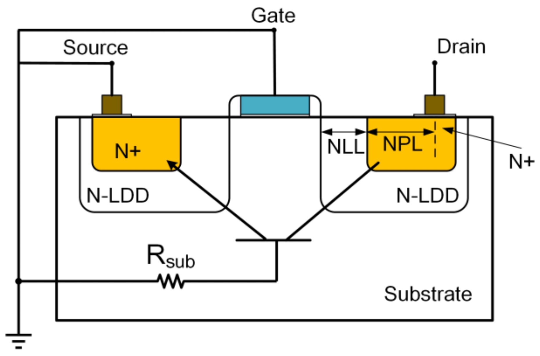
Figure 3.
Layout top view for multi-finger NMOS in ESD clamp (simplified layout, N = 8).

Figure 4.
Schematic of a simplified HBM stress ESD model.
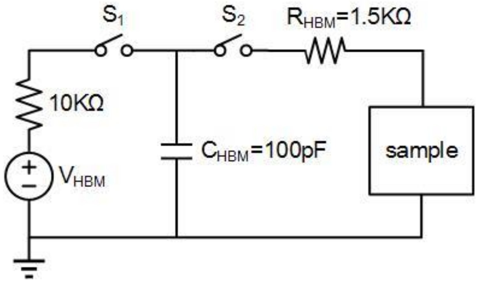
Figure 5.
Burn-out damage observed with SEM of a failed 3D NAND Flash test chip sample.
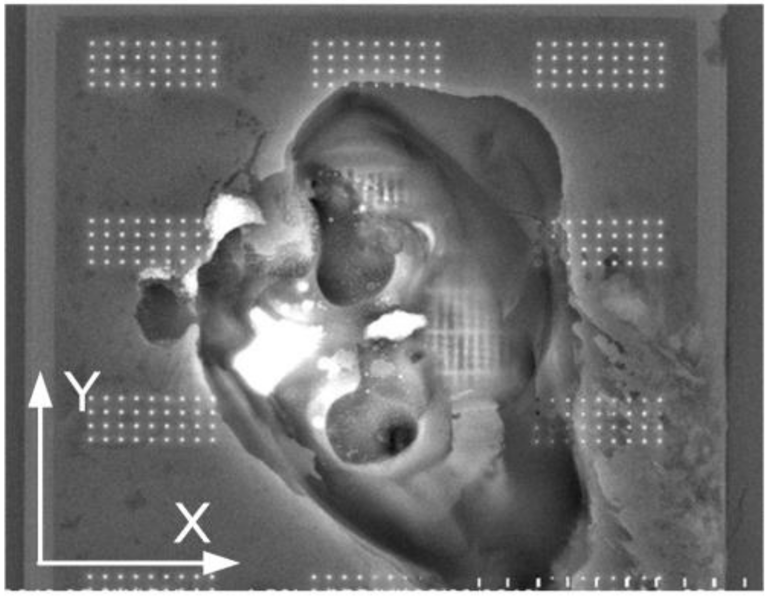
Figure 6.
Measured TLP I-V curve for ESD protection circuit.
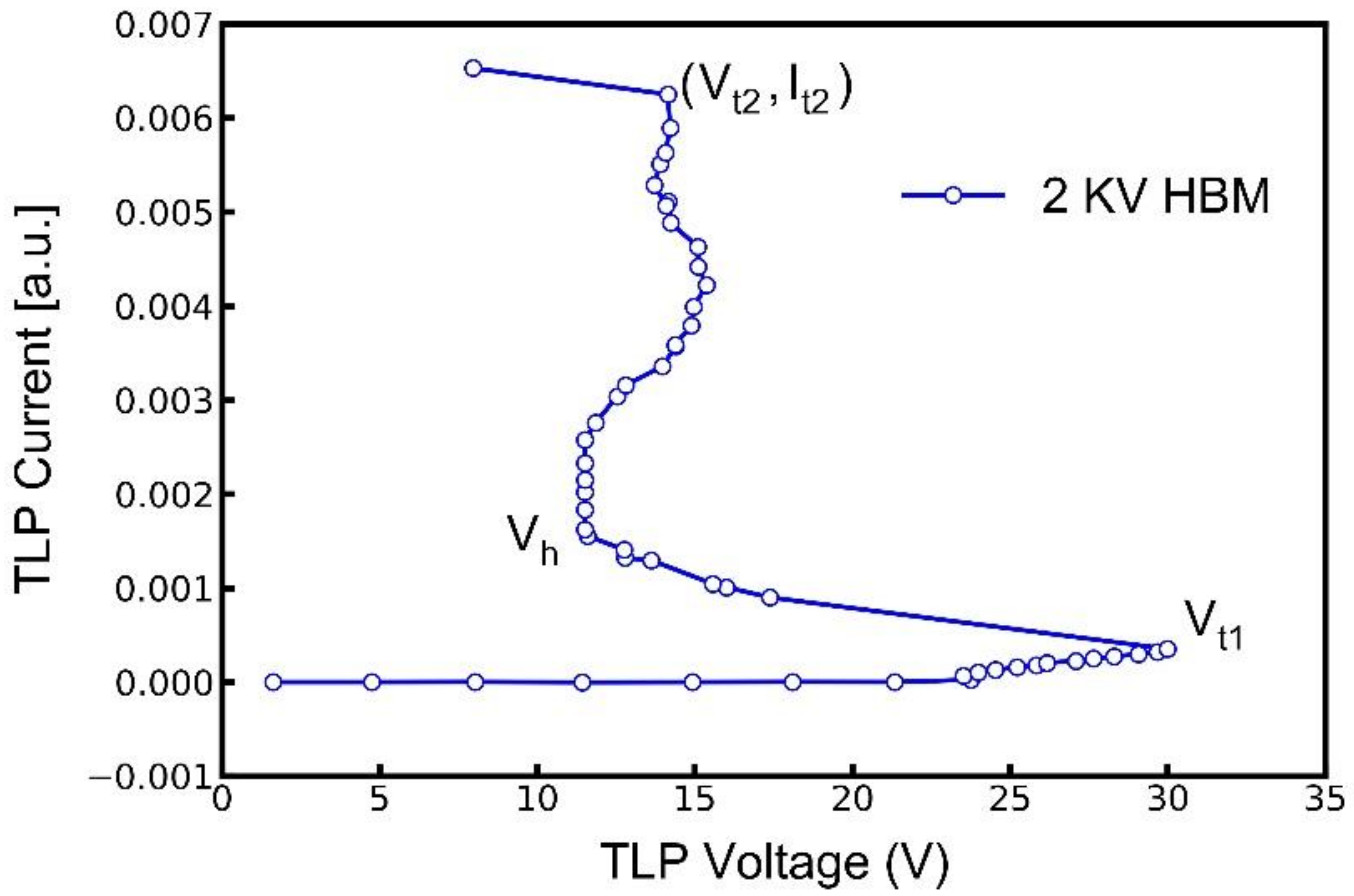
Figure 7.
(a) Equivalent NMOS finger substrate resistance network of 8-finger example layout; (b) substrate resistance network for a single NMOS finger.
Figure 7.
(a) Equivalent NMOS finger substrate resistance network of 8-finger example layout; (b) substrate resistance network for a single NMOS finger.

Figure 8.
Multi-finger NMOS substrate resistance network in ESD clamp.
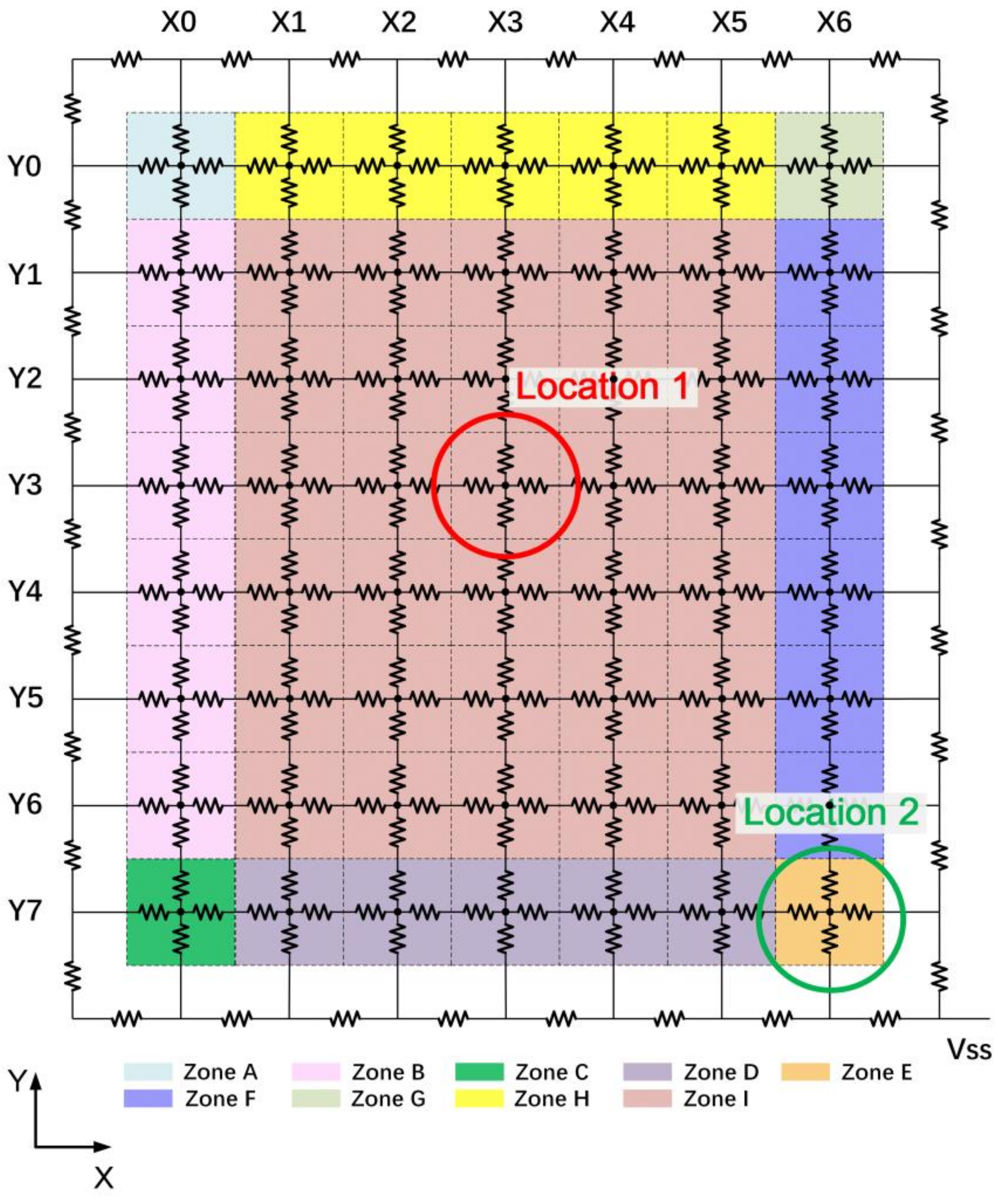
Figure 9.
FIB-sectioned image of the burn-out damage.
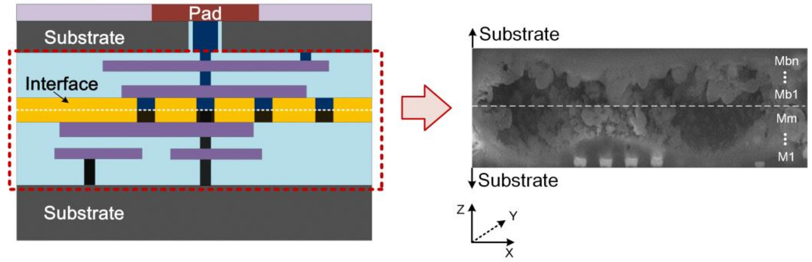
Figure 10.
(a) Crosssection of LDD NMOS depicting various device parameters. IV curves of NMOS with varied (b) N−LLD dose, (c) NLL size, and (d) NPL size obtained using TCAD simulation.
Figure 10.
(a) Crosssection of LDD NMOS depicting various device parameters. IV curves of NMOS with varied (b) N−LLD dose, (c) NLL size, and (d) NPL size obtained using TCAD simulation.
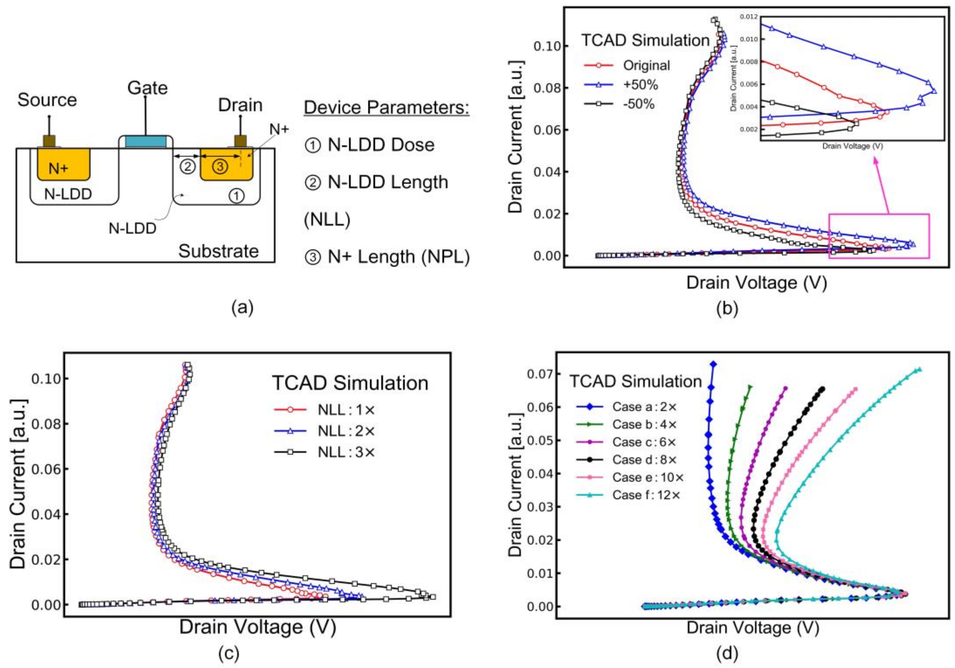
Figure 11.
Cross-section of HV NMOS with extended N+ length.
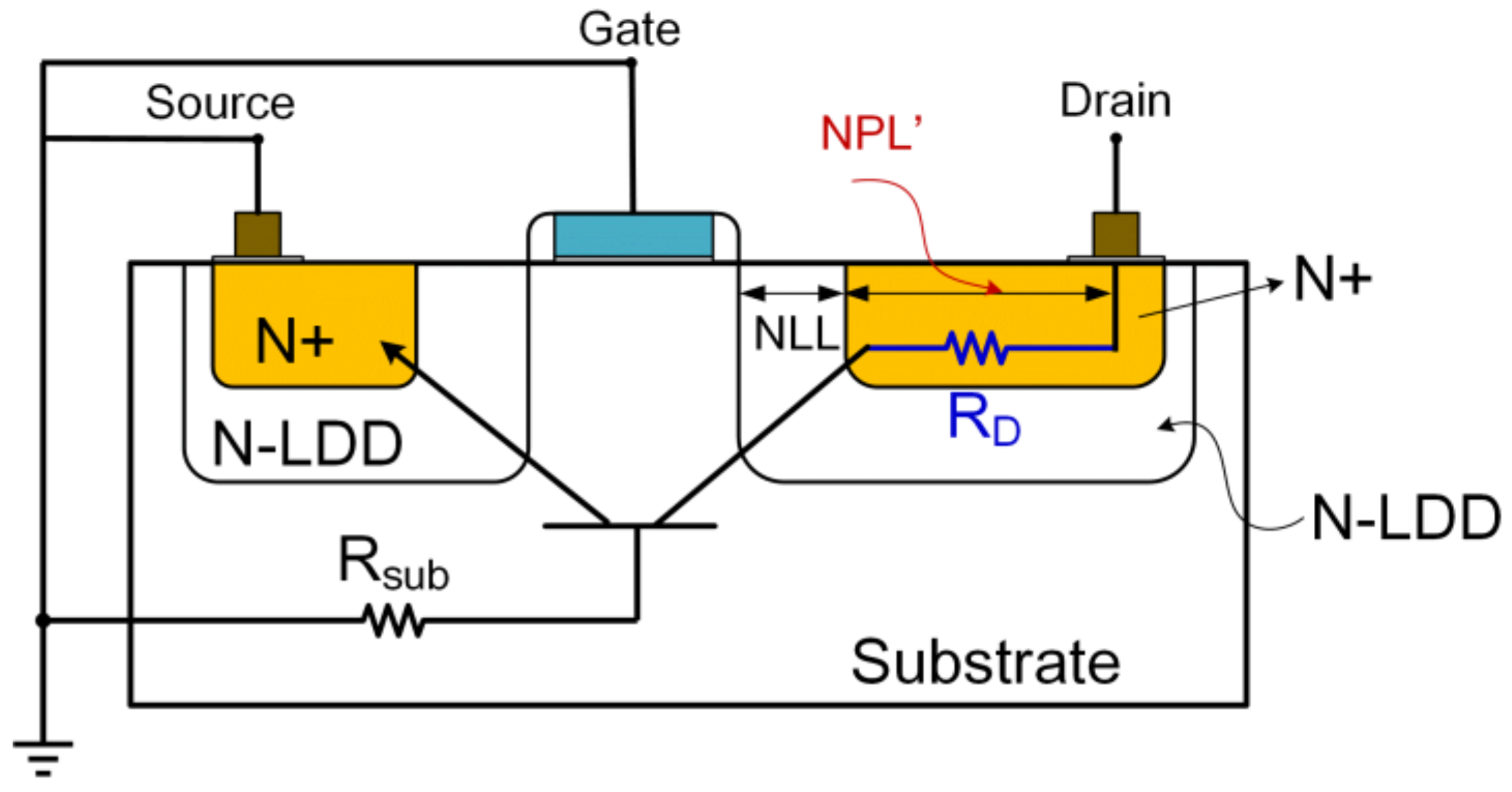
Figure 12.
Contact change for dissipation improvement: (a) original contact count, (b) increased contact count (N = 3), (c) novel contact strip.
Figure 12.
Contact change for dissipation improvement: (a) original contact count, (b) increased contact count (N = 3), (c) novel contact strip.
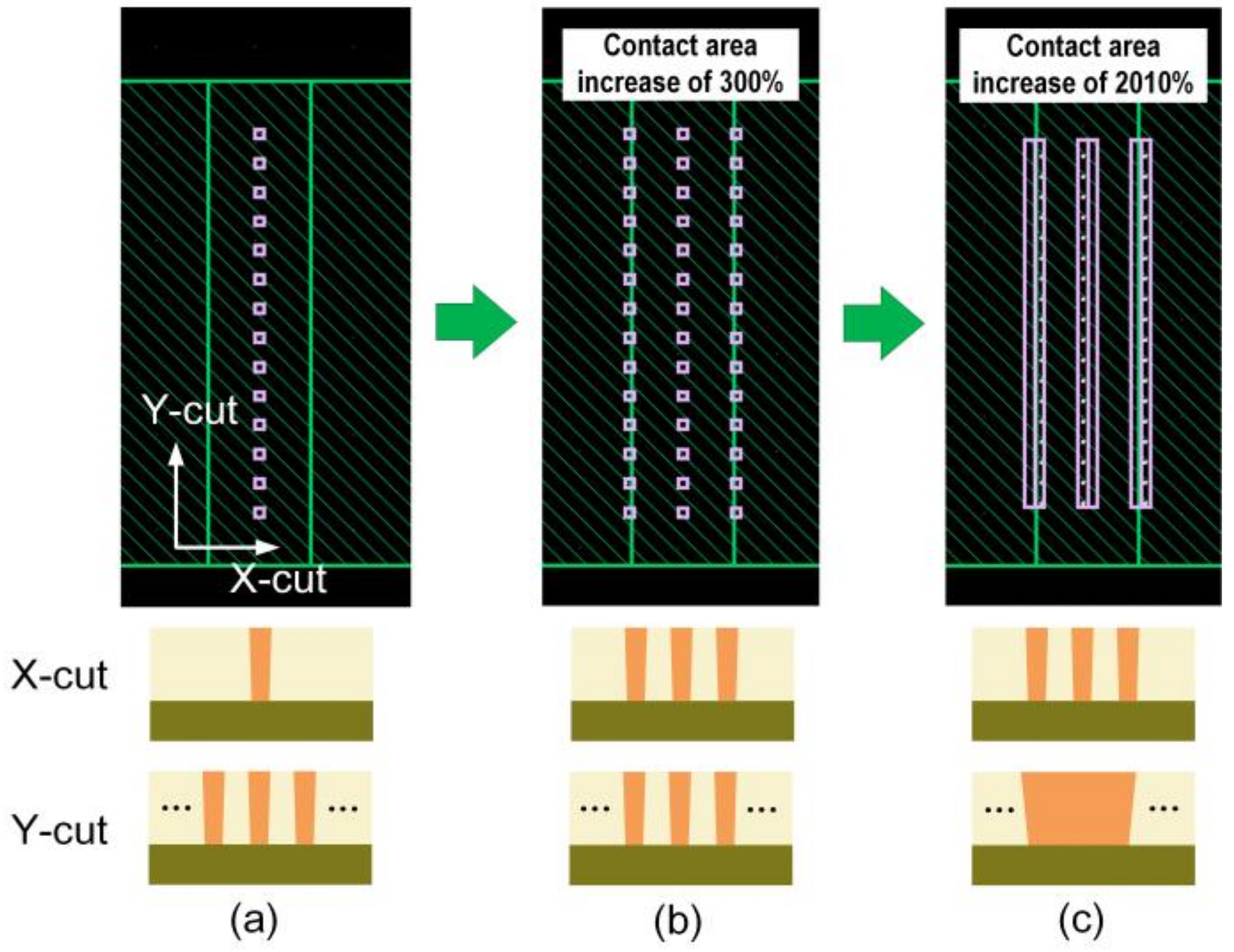
Figure 13.
Measured multi-finger NMOS TLP IV curves with different NPL sizes.


Table 1.
HBM test results with raw test chip samples.
| Sample | Failure Voltage (KV) |
|---|---|
| Sample 1 | 1 |
| Sample 2 | 1.25 |
| Sample 3 | 1.5 |
Table 2.
NMOS finger equivalent substrate resistance by simulation (a.u.).
| X | X0 | X1 | X2 | X3 | X4 | X5 | X6 | |
|---|---|---|---|---|---|---|---|---|
| Y | ||||||||
| Y0 | 6.11 | 6.03 | 5.94 | 5.84 | 5.72 | 5.59 | 5.47 | |
| Y1 | 8.57 | 8.97 | 9.05 | 9.02 | 8.90 | 8.66 | 8.13 | |
| Y2 | 9.19 | 9.82 | 10.06 | 10.08 | 9.95 | 9.61 | 8.87 | |
| Y3 | 9.37 | 10.10 | 10.39 | 10.45 | 10.32 | 9.94 | 9.15 | |
| Y4 | 9.30 | 10.04 | 10.35 | 10.42 | 10.30 | 9.93 | 9.15 | |
| Y5 | 8.97 | 9.65 | 9.91 | 9.97 | 9.88 | 9.57 | 8.86 | |
| Y6 | 8.19 | 8.65 | 8.80 | 8.83 | 8.77 | 8.58 | 8.10 | |
| Y7 | 5.52 | 5.52 | 5.52 | 5.51 | 5.49 | 5.45 | 5.41 | |
Table 3.
HBM test results of a test chip with drain contact improvement.
| Sample | Failure Voltage (KV) |
|---|---|
| Sample 1 | 2 |
| Sample 2 | 2 |
| Sample 3 | 2.5 |
Table 4.
Summary of ESD performance with different device parameters.
| Device Parameter | Vt1 | Vt2 |
|---|---|---|
| N-LDD Dose | √ | × |
| NNL | √ | × |
| NPL | × | √ |
Table 5.
HBM test results with NPL and drain contact improvement.
| Sample | Failure Voltage (KV) |
|---|---|
| Sample 1# | 3.5 |
| Sample 2# | 3.5 |
| Sample 3# | 3.5 |
Publisher’s Note: MDPI stays neutral with regard to jurisdictional claims in published maps and institutional affiliations. |
© 2022 by the authors. Licensee MDPI, Basel, Switzerland. This article is an open access article distributed under the terms and conditions of the Creative Commons Attribution (CC BY) license (https://creativecommons.org/licenses/by/4.0/).
Share and Cite
MDPI and ACS Style
Song, B.; Li, Z.; Wang, X.; Fu, X.; Liu, F.; Jin, L.; Huo, Z. Analysis of HBM Failure in 3D NAND Flash Memory. Electronics 2022, 11, 944. https://doi.org/10.3390/electronics11060944
AMA Style
Song B, Li Z, Wang X, Fu X, Liu F, Jin L, Huo Z. Analysis of HBM Failure in 3D NAND Flash Memory. Electronics. 2022; 11(6):944. https://doi.org/10.3390/electronics11060944
Chicago/Turabian StyleSong, Biruo, Zhiguo Li, Xin Wang, Xiang Fu, Fei Liu, Lei Jin, and Zongliang Huo. 2022. "Analysis of HBM Failure in 3D NAND Flash Memory" Electronics 11, no. 6: 944. https://doi.org/10.3390/electronics11060944
Note that from the first issue of 2016, this journal uses article numbers instead of page numbers. See further details here.