Article

Analysis of Series-Parallel (SP) Compensation Topologies for Constant Voltage/Constant Current Output in Capacitive Power Transfer System

1
School of Rail Transit, Chongqing Vocational College of Public Transportation, Chongqing 402247, China
2
School of Electrical Engineering, Southwest Jiaotong University, Chengdu 611756, China
*
Author to whom correspondence should be addressed.
Electronics 2023, 12(1), 245; https://doi.org/10.3390/electronics12010245
Submission received: 19 November 2022 / Revised: 9 December 2022 / Accepted: 12 December 2022 / Published: 3 January 2023
(This article belongs to the Special Issue Wireless Power Transfer and Wireless Energy Harvest)

Abstract

:
This paper analyzed the four series-parallel (SP) compensation topologies to achieve constant current (CC) and voltage (CV) output characteristics and zero phase angle (ZPA) input conditions with fewer compensation components in the capacitive power transfer (CPT) system. There are three main contributions. Firstly, the universal methodology of SP compensation topologies was constructed to achieve CC, CV output, and ZPA conditions. Secondly, four specific SP compensation topologies were investigated and summarized, including double-sided LC, double-sided CL, CL−LC, and LC−CL topologies. Their input–output characteristics are provided, and system efficiency is analyzed. Thirdly, the CL−LC and LC−CL topologies were proposed to realize ZPA conditions under CC and CV output without any external regulating circuit. A CV output LC−CL experiment prototype was implemented to validate the theoretical analysis.

1. Introduction

Wireless power transfer (WPT) technology utilizing different energy carriers to transfer electric power without physical contact has been a research hotspot recently due to its advantages of flexibility and safety [1,2,3,4]. Inductive power transfer (IPT) and capacitive power transfer (CPT) technologies are two main effective methods among WPT systems to deliver power wirelessly [5]. IPT system using high−frequency magnetic fields to transfer power has been employed in miscellaneous applications, such as biomedical implants [6,7], wireless charging for consumer electronics (CE) [8], electric vehicles (EVs) [9,10,11,12], and unmanned aerial vehicles (UAVs) [13,14]. As a result of the high−frequency magnetic fields generated around the coupler structure in the IPT system, undesirable eddy current loss would be induced in the metallic conductors shown around the IPT system [15]. In addition, the IPT system usually adopts a coupler structure consisting of the expensive Litz wire and ferrite core, increasing the system’s costs and weight [16,17]. Unlike IPT technology, a CPT system using electrical fields as an energy carrier has the advantages of low eddy current loss, lightweight, and good tolerance to metal disturbance [18]. Therefore, the CPT system is more suitable for metal environmental and lightweight applications.
A CPT system usually consists of a power electronic converter, coupler structure, and compensation topologies [19]. The converter (high-frequency inverter and rectifier) supplies the AC signal to compensation topologies. It converts the alternating current to DC load. The coupler structure realizes the wireless power transfer by generating high-frequency electric fields between the transmitting and receiving plates. A capacitive coupler structure would induce significant reactive power in the CPT system, degrading the power transfer capability [20,21,22]. Therefore, the compensation topologies play an essential role in eliminating the reactive power induced by the capacitive coupler [23,24,25,26]. For most charging applications, the output characteristics of constant current (CC) and constant voltage (CV) are significant targets to extend battery life and ensure stable charging, which can also be achieved by appropriate selections of compensation topologies [27]. Furthermore, the parameters design of the compensation circuit can not only adjust the output voltage and current gain but also optimize the system efficiency [28].
Currently, the research on compensation topologies in the CPT system can be divided into basic compensated circuits and high-order compensated circuits [29,30,31,32,33,34,35,36,37,38,39,40]. The basic compensated circuits are composed of series (S) compensation, parallel (P) compensation, and series-parallel (SP) compensation, as shown in Figure 1. As the coupled capacitances of the coupler structure in the CPT system are usually the pF-level, the compensation inductors in the series compensated circuit would be large and heavy [29]. In addition, the structure of the parallel compensated circuit limited the port voltage on coupler plates, which imposed restrictions on transfer power [30]. Hence, the SP compensation and high-order compensation topologies are preferred by researchers [33,34,35,36,37,38,39]. Lu et al. proposed double-sided LCLC [29], double-sided CLLC [34], and double-sided LCL compensation topologies [30] to reduce the resonant inductance and increase the port voltage on the plates. At the same time, the plenty of external compensation components increased the system’s complexity. They made the CPT system lose its advantages of lightness. Then, as one of the SP compensation topologies, the double-sided LC compensation circuit was proposed to achieve CC and CV output with only four external compensation components (half the number of double-sided LCCL topologies). However, when the parameters of double-sided LC are designed to achieve CV output, the zero phase angle (ZPA) condition between the input driving current and driving voltage cannot be realized, which would degrade the power transfer capability.
This paper analyzed the four SP compensation topologies to achieve CC and CV output characteristics and ZPA input conditions with fewer compensation components in the CPT system. There are three main contributions. Firstly, the universal methodology of SP compensation topologies was constructed to achieve CC, CV output, and ZPA conditions. Secondly, four specific SP compensation topologies were investigated and summarized, including double-sided LC, double-sided CL, CL−LC, and LC−CL topologies. Their input–output characteristics are provided, and system efficiency is analyzed. Thirdly, the CL−LC and LC−CL topologies were proposed to realize ZPA conditions under CC and CV output without any external regulating circuit. A CV output LC−CL experiment prototype was implemented to validate the theoretical analysis.

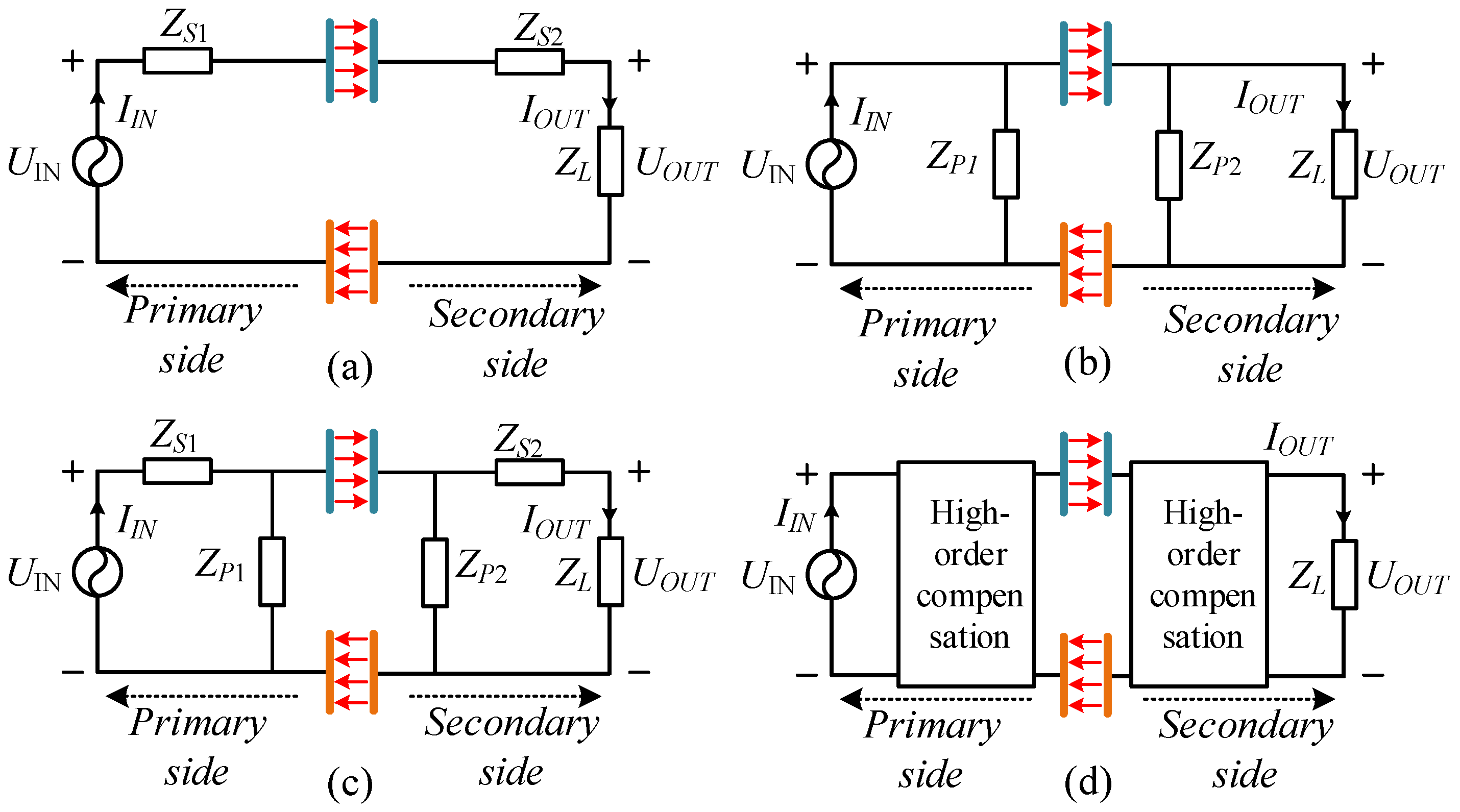
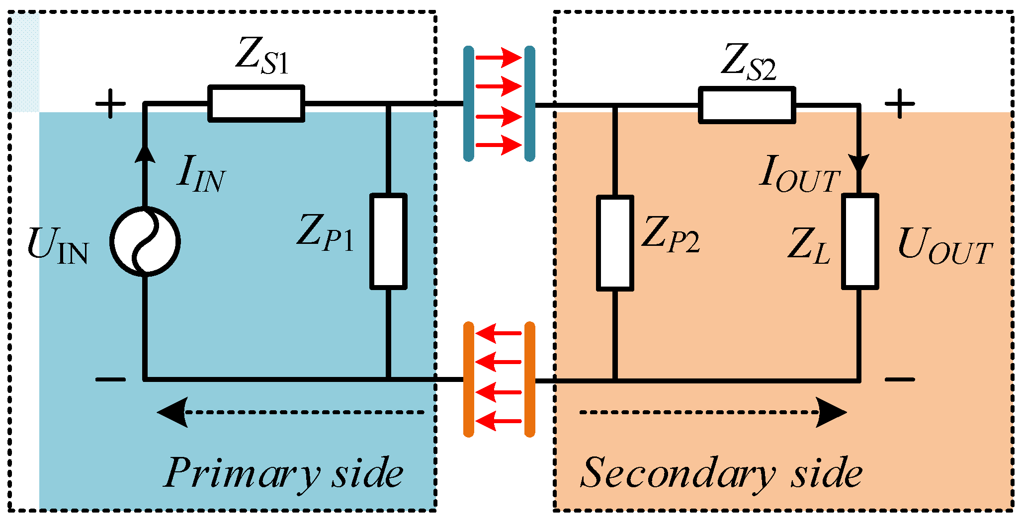
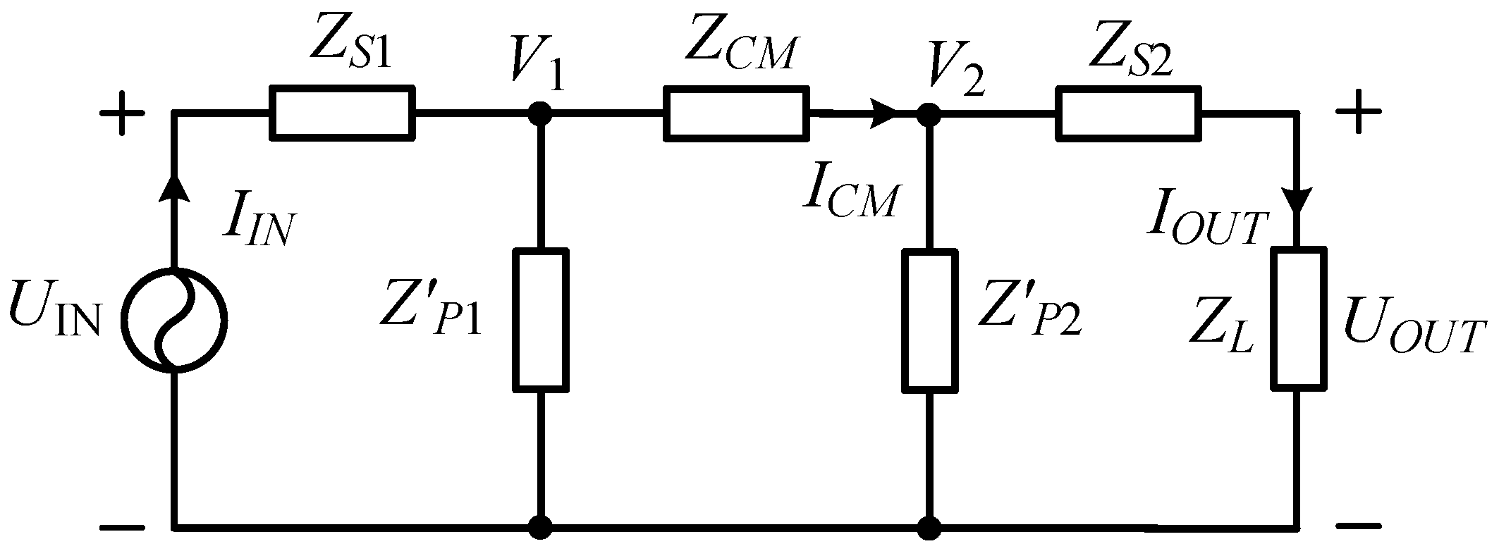
2. Modeling of SP—Based CPT Topology

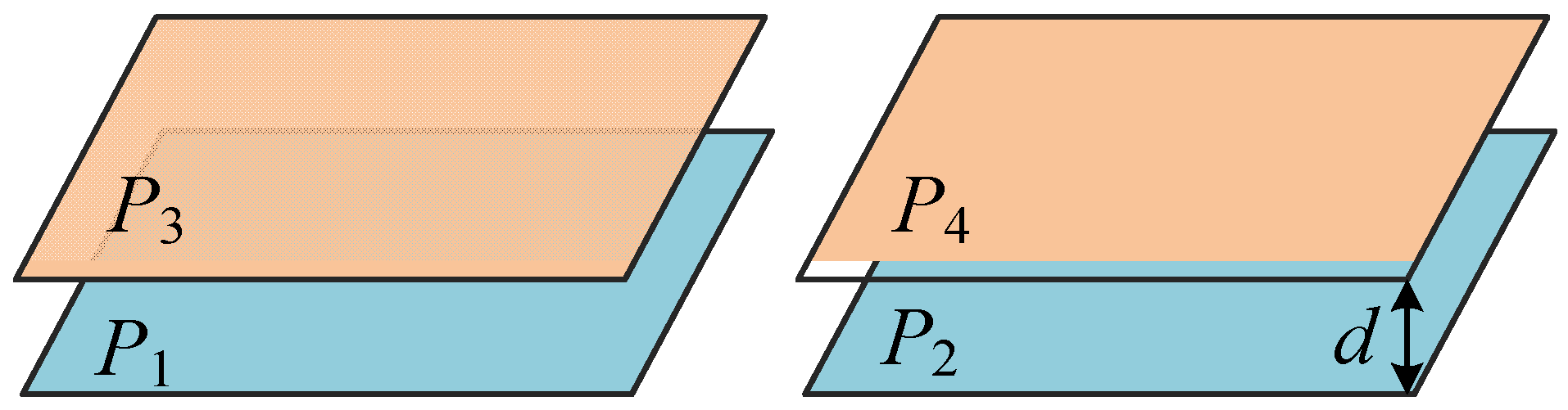
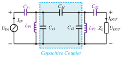
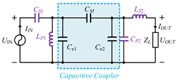
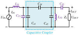
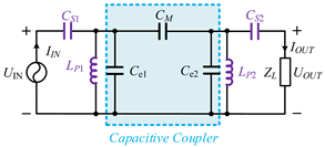
2.1. The Capacitive Coupler Structure

The most widely used coupler structure in the CPT system is shown in Figure 2, which is formed by two pairs of metal plates (P1, P2, P3, P4) stacked by each other with no contact. The distance d between P1 and P3 or P2 and P4 is the so−called transmission distance. Coupling capacitors Cij (i, j = 1, 2, 3, 4) are formed between plates Pi and Pj (i, j = 1, 2, 3, 4), which can be calculated as expressed in Equation (1):
C = ε r S 4 π k d
where εr represents the relative dielectric constant, S is the coupling area of coupler plates, and k represents the electrostatic constant. Therefore, Figure 3a shows the full-capacitor model of the four-plate capacitive structure and the equivalent induced current source model is shown in Figure 3b. The relationships of port voltage V1, V2, and current I1, I2 are expressed as follows.
{ I 1 = j ω C 1 V 1 j ω C M V 2 I 2 = j ω C 2 V 2 j ω C M V 1
According to Equation (2), the simplified π-type and T-type models of the four-plate structure are presented in Figure 4, where the capacitance value satisfied the expressions shown in Equations (3) and (4):
{ C M = C 13 C 24 C 14 C 23 C 13 + C 23 + C 14 + C 24 C 1 = C 12 + ( C 13 + C 14 ) ( C 23 + C 24 ) C 13 + C 14 + C 23 + C 24 C 2 = C 34 + ( C 13 + C 23 ) ( C 14 + C 24 ) C 13 + C 14 + C 23 + C 24
{ C a = C e 1 C e 2 + C e 1 C M + C e 2 C M C e 2 C b = C e 1 C e 2 + C e 1 C M + C e 2 C M C e 1 C c = C e 1 C e 2 + C e 1 C M + C e 2 C M C M .
where Ce1 = C1CM, Ce2 = C2CM. This paper only introduced the classical four-plate capacitive structure due to space constraints. Other structures are not included, such as six−plates, matrixed plates, etc.

2.2. The SP Compensation Topologies

The SP compensation topology in the CPT system is shown in Figure 5, where UIN represents the output AC voltage of the high-frequency inverter, and ZL is the input impedance of the rectifier. It should be mentioned that ZL is resistive when the parasitic impedances of the rectifier are neglected, and the load can be considered as resistance. ZS1 and ZS2 represent the series compensation elements of the primary and secondary sides, respectively. The paralleled compensation elements of the primary and secondary sides are named ZP1 and ZP2.
When UIN is designed to be constant, the input source is considered a constant voltage source. The equivalent circuit is shown in Figure 6 by substituting the π-type model of the coupler structure into the SP compensation topology CPT system. ZP1 and ZP2 are composed of the self−capacitance (C1CM) and ZP1 as well as (C2CM) and ZP2, respectively, which satisfy the expressions as follows.
{ Z P 1 = Z P 1 Z P 1 j ω ( C 1 C M ) + 1 Z P 2 = Z P 2 Z P 2 j ω ( C 2 C M ) + 1
According to Kirchhoff’s law, the SP circuit can be expressed as
[ U I N 0 0 ] = [ Z 11 Z 12 0 Z 21 Z 22 Z 23 0 Z 32 Z 33 ] · [ I I N I C M I O U T ]
where Z11 = ZS1 + ZP1, Z12 = −ZP1, Z21 = −ZP1, Z22 = ZP1 + ZP2 + ZCM, Z23 = −ZP2, Z32 = −ZP2, Z33 = ZP2 + ZS2 + ZL. The output voltage UOUT and output current IOUT can be calculated according to Equation (6), which can be written as
{ U O U T = U I N Z 12 Z 23 Z L ( Z P 2 + Z S 2 + Z L ) ( Z 12 2 Z 11 Z 22 ) + Z 11 Z 23 2 I O U T = U I N Z 12 Z 23 ( Z P 2 + Z S 2 + Z L ) ( Z 12 2 Z 11 Z 22 ) + Z 11 Z 23 2
To achieve CC output characteristics, the following conditions need to be satisfied.
Z 12 2 Z 11 Z 22 = 0 Z P 1 + Z S 1 / / ( Z C M + Z P 2 ) = 0
Then, the input impedance ZIN and the output current IOUT can be derived as
{ Z I N = Z 11 Z 23 2 Z 23 2 Z 22 Z 33 I O U T = U I N Z 12 Z 11 Z 23
The condition to achieve CV output characteristics is expressed as follows
( Z P 2 + Z S 2 ) ( Z 12 2 Z 11 Z 22 ) + Z 11 Z 23 2 = 0
The following condition Equation (11) can be obtained to achieve CV output by simplifying Equation (10).
{ Z S 1 + Z P 1 = 0 Z S 2 + Z P 2 = 0
The input impedance ZIN and the output voltage UOUT can also be calculated as
{ Z I N = Z 11 + Z 33 Z 12 2 Z 23 2 Z 22 Z 33 U O U T = U I N Z 12 Z 23 Z 12 2 Z 11 Z 22
When the inverter’s output current is constant, the CC or CV output condition can also be derived according to the above theory. The compensation parameters to achieve CC output should satisfy the following equation:
Z 22 = 0 Z P 1 + Z C M + Z P 2 = 0
The current gain can be calculated as
G I = | I O U T I I N | = | Z P 1 Z P 2 | = | Z 12 Z 23 |
Then, the input impedance ZIN can be derived as
Z I N = Z 11 + G I 2 Z 33
The condition to achieve CV output characteristics with a constant current input source can be deduced based on the reciprocity of CC output with a constant voltage input source, which is presented as follows.
Z 23 2 ( Z 33 Z L ) Z 22 = 0 Z P 2 + Z S 2 / / ( Z C M + Z P 1 ) = 0
Similarly, the output voltage UOUT and the input impedance ZIN can be derived as
{ U O U T = Z P 1 ( Z S 2 + Z P 2 ) Z P 2 I I N Z I N = Z P 1 2 ( Z S 2 + Z P 2 ) Z L Z 22 + Z S 1 + Z P 1 ( Z C M + Z P 2 ) Z 22
To explicitly demonstrate the output characteristics of SP compensation topologies, we have concluded the above theories in Table 1. Table 1 shows the conditions for realizing CC output or CV output of the CPT system based on the SP compensation network when the input source is a constant current source or a constant voltage source, and the expression of system current or voltage gain under corresponding conditions. The following section will analyze the specific SP-based compensation topology. As most application scenarios adopted the voltage−driven inverter, and the circuit characteristics of SP compensation with constant current input are similar to that of constant voltage input, the circuit analysis of the constant current input source is not included in this paper.

3. Circuit Analysis of Specific SP Topology

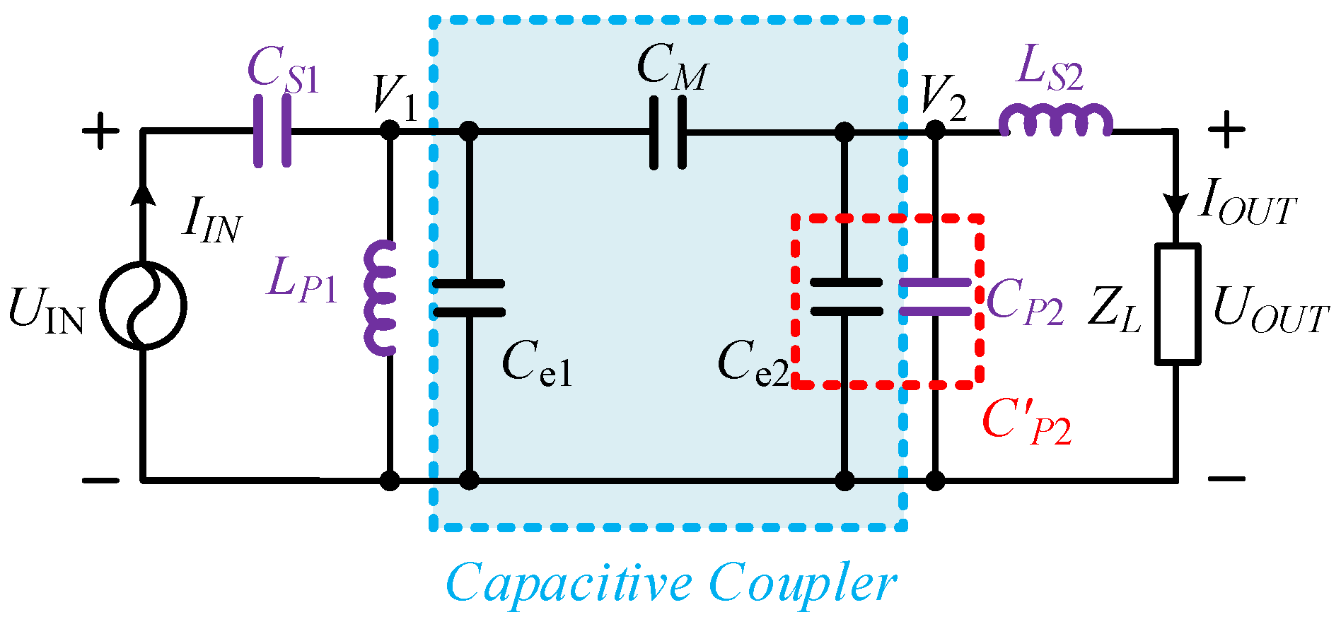
3.1. Double-Sided LC Compensation Topology

Figure 7 shows the double-sided LC compensation topology with the π-type model of capacitive coupler structure, where LS1 and LS2 are the series compensation inductors and CP1 and CP2 are the paralleled compensation capacitors. Generally, large capacitance CP1 and CP2 are paralleled on the coupler structure to eliminate the impact of variation of Ce1 and Ce2. To achieve CC output characteristics, the derivation in Equation (8) can be rewritten as
ω 2 L S 1 = C P 2 + C M C P 1 C P 2 + C P 1 C M + C P 2 C M
where C′P1 = CP1 + Ce1, C′P2 = CP2 + Ce2. Then, the output current can be calculated as
I O U T = j ω C P 1 C P 2 + C P 1 C M + C P 2 C M C M U I N
The input impedance ZIN of double-sided LC compensation with CC output characteristics can be calculated through Equation (9), and the condition to achieve ZPA operation is derived as
ω 2 L S 2 = C P 1 + C M C P 1 C P 2 + C P 1 C M + C P 2 C M
Similarly, the condition to achieve CV output characteristics can be derived through Equation (10), which is expressed as
{ ω 2 L S 1 = 1 C P 1 + C e 1 ω 2 L S 2 = 1 C P 2 + C e 2
The voltage gain of double-sided LC compensation topology is presented as follows.
G V = C P 1 + C e 1 C P 2 + C e 2
The input impedance ZIN of double-sided LC compensation with CV output characteristics can also be calculated as
Z I N = 1 G V 2 / Z L j ω C P 1 ( C P 1 / C M + C P 1 / C P 2 + 1 )
As the result of CP1/CM + CP1/CP2 + 1 > 0, there is always an imaginary part in ZIN, which means the ZPA operation cannot be achieved with CV output characteristics.

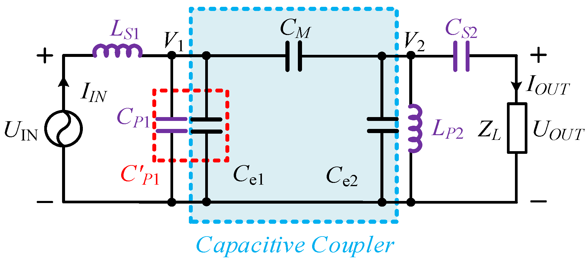
3.2. Double-Sided CL Compensation Topology

The double-sided CL compensation topology is presented in Figure 8, where compensation inductors LP1 and LP2 are paralleled on the coupler structure, and compensation capacitors CS1 and CS2 are series with the coupler structure. ZP1 and ZP2 are composed of LP1 and Ce1, LP2 and Ce2 in parallel, respectively. ZS1 and ZS2 represent the capacitive reactance of CS1 and CS2. To achieve CC output characteristics, the derivation in Equation (8) can be rewritten as
{ ω 2 L P 1 = C e 2 C S 1 C e 2 + C e 1 C e 2 + C e 1 C M + C e 2 C M ω 2 L P 2 = C e 1 C e 1 C e 2 + C e 1 C M + C e 2 C M
When the compensation elements satisfy the expression in Equation (24), the output current can be calculated as
I O U T = j ω C S 1 C e 2 C e 1 U I N
Then the input impedance ZIN can be deduced as
Z I N = 1 j ω ( C c + C b C b ω 2 L P 2 C S 2 ) + C b L P 2 Z L
where the expression Cb and Cc is shown in Equation (4). ZPA operation condition of double-sided CL compensation topology can be achieved when the reactive part of ZIN is eliminated. Hence the following equation is derived from Equation (24).
C S 2 = C b 2 C c + C b
Same with the previous analysis, to achieve CV output characteristics, the compensation elements should satisfy the condition as
{ ω 2 L P 1 = C e 2 C S 1 C e 2 + C e 1 C e 2 + C e 1 C M + C e 2 C M ω 2 L P 2 = C e 1 C S 1 C e 1 + C e 1 C e 2 + C e 1 C M + C e 2 C M
The voltage gain GV is given by
G V = C S 1 C e 2 C S 2 C e 1
The input impedance ZIN with CV output characteristics is deduced by
Z I N = 1 / ω 2 C S 1 2 1 + ( C e 2 C e 1 ) 2 ( 1 1 ω 2 C S 2 2 Z L ) j C c ω C a 2
where Ca is expressed in Equation (4), as Cc is not equal to zero, the input impedance consists of the real and imaginary parts. Therefore, the ZPA cannot be realized under the CV mode of double-sided CL compensation topology.

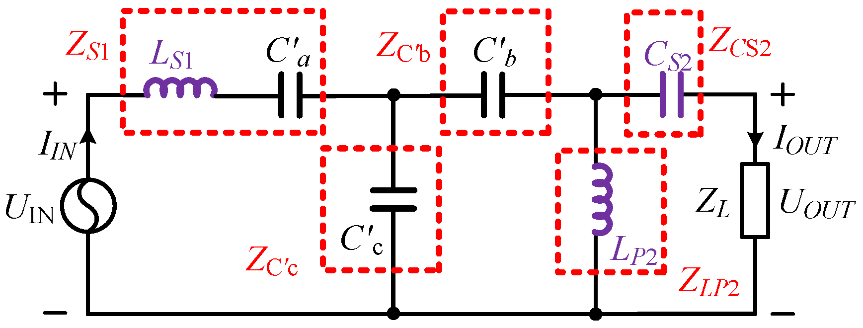
3.3. CL−LC Compensation Topology

The CL−LC compensation topology with π-type coupler model is presented in Figure 9, CS1, and LS2 represent the series compensation capacitor on the primary side and the inductor on the secondary side, respectively. LP1 and CP2 are the compensation inductor and capacitor paralleled in the primary and secondary ports of the coupler structure, respectively. To simplify the analysis, the π-type coupler model is transferred to the T-type circuit, as shown in Figure 10.
As shown in Figure 10, the impedances corresponding with Figure 5 are circled by a red box. Then, the Z11, Z12, Z22 of Figure 10 can be rewritten as
{ Z 11 = 1 j ω C S 1 + j ω L P 1 Z 12 = j ω L P 1 Z 22 = 1 j ω C a + 1 j ω C c + j ω L P 1
The values of Ca, Cb, and Cc are given by
{ C a = C e 1 C P 2 + C e 1 C M + C P 2 C M C P 2 C b = C e 1 C P 2 + C e 1 C M + C P 2 C M C e 1 C c = C e 1 C P 2 + C e 1 C M + C P 2 C M C M .
where CP2 = Ce2 + CP2. Therefore, the CC mode of CL−LC compensation topology is derived as
ω 2 L P 1 = ( 1 C a + 1 C c ) 1 C S 1 1 C a + 1 C c + 1 C S 1
The expression of Equation (33) can be simplified as ZLP1 = (ZC′a + ZC′c)//ZCS1, where ZLP1 = jωLP1, ZC′a = jωC′a, ZC′c = jωC′c, ZCS1 = jωCS1. The output current IOUT under CC output characteristics is given by
I O U T = j ω ( 1 + C c C a ) U I N
The condition to achieve ZPA of CL−LC topology with CC output can be deduced by
ω 2 L P 2 = 1 C b + 1 C c C a C c C a + C c ( 1 + C a C c ( C a + C c ) C S 1 )
Then the input impedance ZIN is expressed by
Z I N = C a C c Z L C S 1 ( C a + C c )
According to Equation (10), the condition to achieve CV output characteristics of CL−LC topology is calculated as
{ ω 2 L P 1 = 1 C S 1 = 1 C a + 1 C c ω 2 L S 2 = 1 C b + 1 C c
The voltage gain GV is given by
G V = C S 1 C c
The input impedance ZIN is given by
Z I N = ω 4 C c 2 L P 1 2 Z L
It can be concluded from Equations (36) and (39) that the ZPA operation condition can be achieved under arbitrary resistance value of ZL in CC or CV mode of CL−LC compensation topology.

3.4. LC−CL Compensation Topology

The LC−CL compensation topology with the π-type equivalent circuit of the capacitive coupler structure is shown in Figure 11. LS1 and CS2 represent the series compensation inductor and capacitor, respectively. CP1 and LP2 represent the paralleled compensation capacitor and inductor, respectively. Similar to the analysis of CL−LC topology, the LC−CL compensation topology with a T-type coupler model is shown in Figure 12, where Ca, Cb, and Cc is given by
{ C a = C P 1 C e 2 + C P 1 C M + C e 2 C M C e 2 C b = C P 1 C e 2 + C P 1 C M + C e 2 C M C P 1 C c = C P 1 C e 2 + C P 1 C M + C e 2 C M C M .
The condition to achieve CC output, as shown in Equation (8) can be rewritten as
Z C c 2 ( Z S 1 + Z C c ) ( Z C c + Z C b + Z L P 2 ) = 0
By solving Equation (41), the compensation elements to realize CC output can be derived as
{ ω 2 L S 1 = 1 C a ω 2 L P 2 = 1 C b
Then the output current IOUT is deduced by
I O U T = j U I N ω L P 2
The input impedance ZIN under CC output condition is calculated as
Z I N = 1 ( ω C b ) 2 Z L + j [ ω C b ( 1 C b C S 2 ) + ω C c ]
It can be seen that the input impedance consists of an imaginary and a real part. Therefore, the following expression can be derived to achieve ZPA operation with CC output characteristics.
ω C b ( 1 C b C S 2 ) + ω C c = 0 C S 2 = C b 2 C b + C c
According to Equation (10), the CV output condition can be deduced as
{ ω 2 L S 1 = 1 C a + 1 C c ω 2 L P 2 = 1 C S 2
Then the voltage gain GV is derived as
G V = C c C S 2
When the compensation inductor LP2 satisfies (48), the ZPA operation can be achieved, and the input impedance ZPA is given in Equation (48).
{ ω 2 L P 2 = 1 C b + 1 C c Z I N = Z L ω 4 C c 2 L P 2 2
The comparison of each SP-based CPT compensation topology has been listed in Table 2 and Table 3, which show output characteristics, ZPA condition, and compensation conditions to achieve CC or CV output, respectively. To sum up, it can be concluded that all four basic SP compensation topologies can realize the CC and CV output characteristics through properly designing compensation parameters. However, the double-sided LC and double-sided CL topologies cannot realize the ZPA condition when designed to achieve CV output. On the contrary, the CL−LC and LC−CL topologies can achieve ZPA conditions on both the CC output and CV output. Therefore, the following analysis concentrates on the CL−LC and LC−CL topologies due to their advantages of good input characteristics.

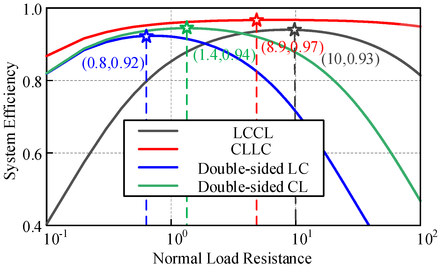
4. Efficiency Analysis of SP-Based CPT Topology

The circuit simplified models of passive components with parasitic resistance are presented in Table 4 [39], where rCS and rLS are the series resistance, rCP and rLP are the paralleled resistance, QC and QL represent the quality factor of compensation capacitors and inductors, respectively. To simplify the efficiency calculation, the circuit model of parasitic resistance should be appropriately adopted according to the specified compensation topology. Figure 13 shows the four basic SP compensation topologies considering the parasitic resistance of passive components. The system efficiency of double-sided LC and double-sided CL compensation topology can be expressed as
{ η | L C L C = | I O U T | 2 Z L | I O U T | 2 Z L + | I O U T | 2 r L S 2 + | I I N | 2 r L S 1 + | V 1 | 2 r C P 1 + | V 2 | 2 r C P 2 η | C L C L = | I O U T | 2 Z L | I O U T | 2 Z L + | I O U T | 2 r C S 2 + | I I N | 2 r C S 1 + | V 1 | 2 r L P 1 + | V 2 | 2 r L P 2
The system efficiency of CL−LC and LC−CL topology can be expressed as
{ η | C L L C = | I O U T | 2 Z L | I O U T | 2 Z L + | I O U T | 2 r L S 2 + | I I N | 2 r C S 1 + | I L P 1 | 2 r L P 1 + | V 2 | 2 r C P 2 η | L C C L = | I O U T | 2 Z L | I O U T | 2 Z L + | I O U T | 2 r C S 2 + | I I N | 2 r L S 1 + | I L P 2 | 2 r L P 2 + | V 1 | 2 r C P 1
The system efficiency of four SP-based compensation topologies can be derived from Equations (49) and (50). Taking the LCCL compensation topology as an example, its AC−AC efficiency is calculated as
η | L C C L = 1 1 + Z L ( ω C P 1 Q C G V 2 + ω C S 2 Q L ) + 1 Z L ( G V 2 ω C a Q L + G V 2 C P 1 C a 2 Q C + Q L + Q C ω C S 2 Q L Q C )
where GV is equal to Cc/CS2, and Ca, Cc are expressed in (40). As shown in Equation (51), when the quality factor and impedance of passive elements are fixed, the efficiency of LCCL topology is decided by the load resistance ZL and system operation frequency ω. Hence, the maximum system efficiency can be derived as
η | L C C L _ max = 1 1 + 2 ( ω C P 1 Q C G V 2 + ω C S 2 Q L ) ( G V 2 ω C a Q L + G V 2 C P 1 C a 2 Q C + Q L + Q C ω C S 2 Q L Q C )
The optimum load resistance to achieve the maximum system efficiency is calculated as follows.
Z L = ( G V 2 ω C a Q L + G V 2 C P 1 C a 2 Q C + Q L + Q C ω C S 2 Q L Q C ) ( ω C P 1 Q C G V 2 + ω C S 2 Q L )
Figure 14 illustrates the system efficiency curves against the variations of load resistance for four SP compensation topologies. The output voltages of the four topologies are designed to be the same. The voltage gains of CLLC and LCCL are 0.2 and 5, respectively. It can be seen that the system efficiency of CLLC topology is the highest among the load variations, which is due to the CLLC topology in CV mode equivalent to the buck converter, leading to the smallest loop current under the same power level. Each compensation topology has an optimum load resistance to achieve the highest system efficiency. The optimum load resistance can be adjusted according to the application requirements.

5. Experimental Verification

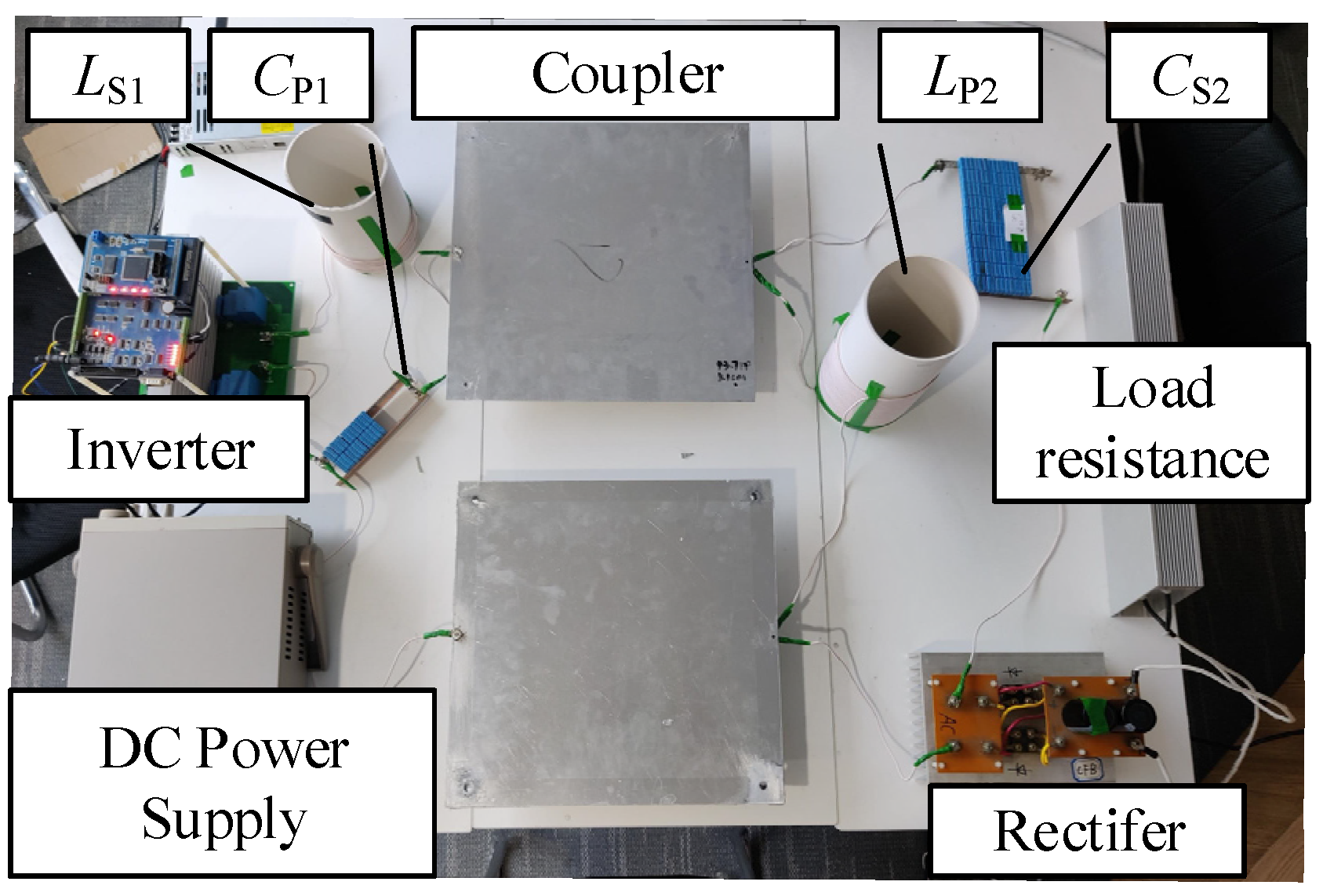
5.1. Experimental Prototype

To verify the proposed theory, an experimental prototype of the CPT system with LCCL compensation topology is built up, as shown in Figure 15. The coupler structure consists of four 300 mm × 300 mm aluminum plates. The transfer distance is set to 5 mm. The switching devices of the full−bridge inverter adopted C2M0160120D MOSFETS, and the MSC020SDA120B−ND diodes were used in the full−bridge rectifier. In order to eliminate the undesirable magnetic loss of ferrite in the traditional inductor, the compensation inductors in the experiment adopted the air−core inductor constructed by PVC tubes wounding with Litz wire. To reduce the size of inductors, the switching frequency of MOSFETS was set to 1 MHz. The system parameters are listed in Table 5.

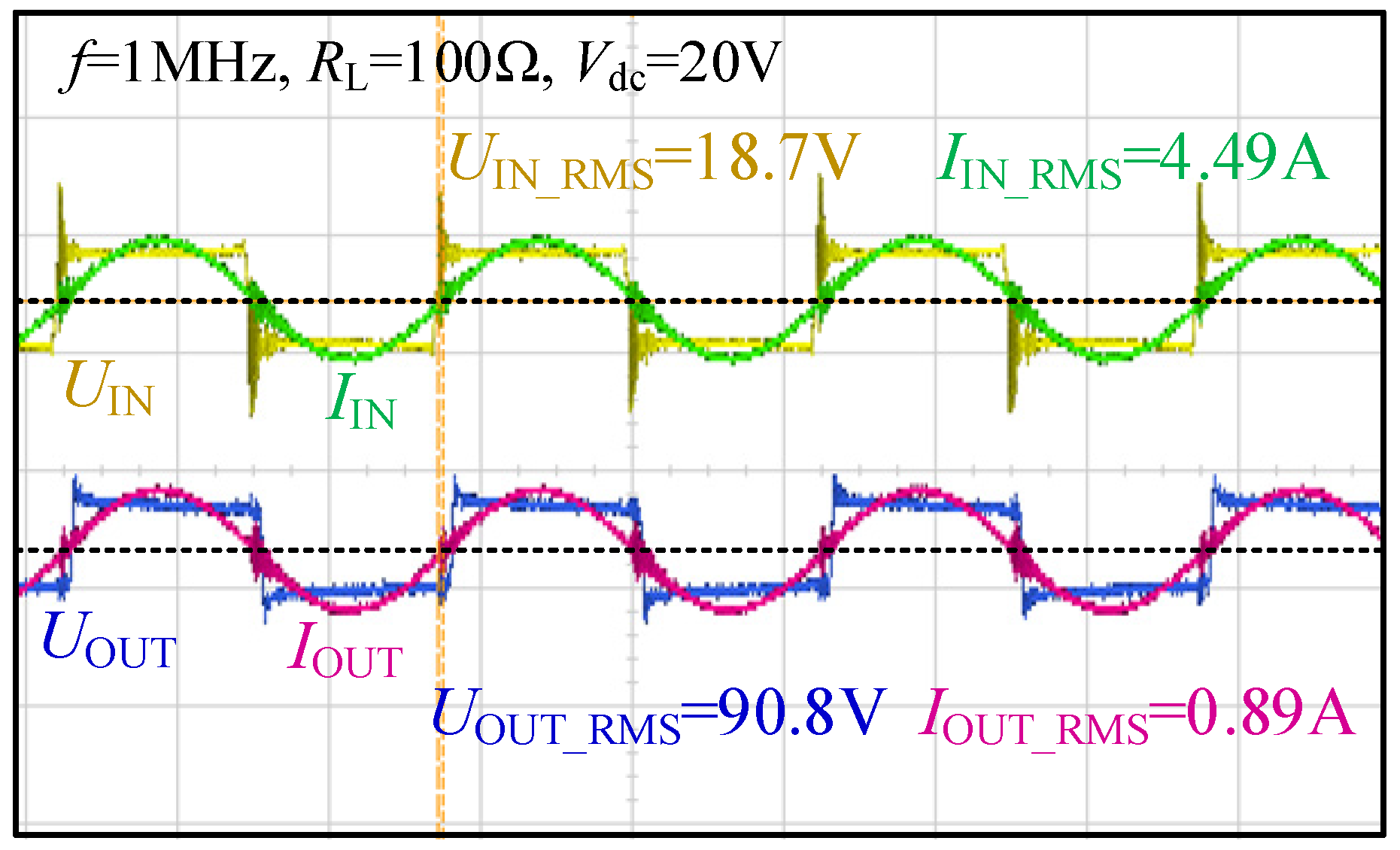
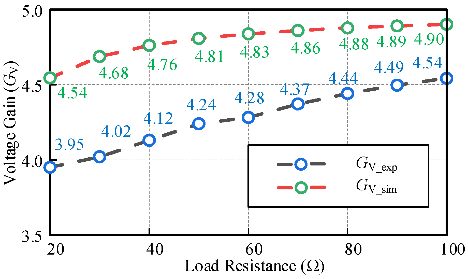
5.2. Experimental Results

When the voltage gain of the LCCL compensation CPT system is designed to 5, the experimental AC waveforms of UIN, IIN, UOUT, and IOUT are shown in Figure 16. The value of UIN, IIN, UOUT, and IOUT is 18.7 V, 4.49 A, 90.8 V, and 0.89 A, respectively. The phase difference between the input voltage and the input current is close to zero degrees, and it can be concluded that the ZPA operation of LCCL topology to achieve CV output is achieved without an extra compensation circuit. As the parasitic resistances of compensation components exist, the measured voltage gain with 100 Ω load resistance is 4.52.
To verify the constant output voltage characteristics, the output voltage gains are measured with load resistance changing from 100 Ω to 20 Ω. The measured results and simulated results are illustrated in Figure 17. The simulated results are conducted in MATLAB/SIMULINK models. When the load resistance increases to 5 times itself, the voltage gain changes from 4.54 to 4.90 in simulation models. While in practice, due to the impact of the parasitic resistance of passive components, the voltage gain increased from 3.95 (79 V) to 4.54 (90.8 V), spaces missing, and the rate of voltage change reached 12.9%. The voltage drop can be reduced in practical applications by adopting compensation elements with more minor resistance and more accurate passive components.
Figure 18 shows the measured system efficiency and output power with changing load resistance. As the output voltage is independent of load resistance, the output power decreased from 334 W to 78 W with load resistance changed from 20 Ω to 100 Ω. Since the losses of the inverter, rectifier, and capacitive coupler are not considered in the calculation of system theoretical efficiency, the system experimental efficiency is obviously lower than the system theoretical efficiency. The system efficiency increased with the increasing load resistance, which is consistent with theoretical analysis. Therefore, the double-sided LC compensation CPT system preferred the heavy load situation. The maximum system efficiency when load resistance changes from 20 Ω to 100 Ω can reach 89% and the system efficiency can be lifted further by using compensation elements with high−quality factors.

6. Conclusions

This paper analyzed the SP compensation topologies in the CPT system to achieve CC/CV output characteristics and ZPA input conditions. The T/П circuit models of the coupler structure were adopted to simplify the regular SP compensation circuit, and the input–output characteristics of four specific SP compensation topologies were derived, respectively. Under CC output conditions, four specific topologies can achieve ZPA input property. In contrast, only CLLC and LCCL topologies can realize the ZPA input when designed to achieve CV output. The system efficiency calculation methodologies were given and analyzed. The experimental verification was carried out, and the ZPA condition and load−independent output characteristics were verified.

Author Contributions

Conceptualization, S.L.; methodology, C.T.; software and hardware preparation, Z.W.; validation, H.C.; writing—original draft preparation, S.L.; writing—review and editing, B.L.; supervision, J.J. All authors have read and agreed to the published version of the manuscript.

Funding

This research was funded by Chongqing Vocational Education Teaching Reform Research Project in 2021 under Grant Z213289.

Data Availability Statement

Not applicable.

Conflicts of Interest

The authors declare no conflict of interest.

References

  1. Zhang, Z.; Pang, H.; Georgiadis, A.; Cecati, C. Wireless Power Transfer—An Overview. IEEE Trans. Ind. Electron. 2019, 66, 1044–1058. [Google Scholar] [CrossRef]
  2. Patil, D.; McDonough, M.K.; Miller, J.M.; Fahimi, B.; Balsara, P.T. Wireless Power Transfer for Vehicular Applications: Overview and Challenges. IEEE Trans. Transp. Electrif. 2018, 4, 3–37. [Google Scholar] [CrossRef]
  3. Luo, B.; Hu, A.P.; Munir, H.; Zhu, Q.; Mai, R.; He, Z. Compensation Network Design of CPT Systems for Achieving Maximum Power Transfer Under Coupling Voltage Constraints. IEEE J. Emerg. Sel. Top. Power Electron. 2022, 10, 138–148. [Google Scholar] [CrossRef]
  4. Luo, B.; Long, T.; Guo, L.; Dai, R.; Mai, R.; He, Z. Analysis and Design of Inductive and Capacitive Hybrid Wireless Power Transfer System for Railway Application. IEEE Trans. Ind. Appl. 2020, 56, 3034–3042. [Google Scholar] [CrossRef]
  5. Dai, J.; Ludois, D.C. A Survey of Wireless Power Transfer and a Critical Comparison of Inductive and Capacitive Coupling for Small Gap Applications. IEEE Trans. Power Electron. 2015, 30, 6017–6029. [Google Scholar] [CrossRef]
  6. Jeong, N.S.; Carobolante, F. Wireless Charging of a Metal-Body Device. IEEE Trans. Microw. Theory Tech. 2017, 65, 1077–1086. [Google Scholar] [CrossRef]
  7. Chen, Q.; Wong, S.C.; Tse, C.K.; Ruan, X. Analysis, Design, and Control of a Transcutaneous Power Regulator for Artificial Hearts. IEEE Trans. Biomed. Circuits Syst. 2009, 3, 23–31. [Google Scholar] [CrossRef]
  8. Hui, S.Y. Planar Wireless Charging Technology for Portable Electronic Products and Qi. Proc. IEEE 2013, 101, 1290–1301. [Google Scholar] [CrossRef] [Green Version]
  9. Luo, B.; Long, T.; Mai, R.; Dai, R.; He, Z.; Li, W. Analysis and design of hybrid inductive and capacitive wireless power transfer for high-power applications. IET Power Electron. 2018, 11, 2263–2270. [Google Scholar] [CrossRef]
  10. Nagendra, G.R.; Chen, L.; Covic, G.A.; Boys, J.T. Detection of EVs on IPT Highways. IEEE J. Emerg. Sel. Top. Power Electron. 2014, 2, 584–597. [Google Scholar] [CrossRef]
  11. Covic, G.A.; Boys, J.T. Modern Trends in Inductive Power Transfer for Transportation Applications. IEEE J. Emerg. Sel. Top. Power Electron. 2013, 1, 28–41. [Google Scholar] [CrossRef]
  12. Moon, H.; Kim, S.; Park, H.H.; Ahn, S. Design of a Resonant Reactive Shield With Double Coils and a Phase Shifter for Wireless Charging of Electric Vehicles. IEEE Trans. Magn. 2015, 51, 1–4. [Google Scholar] [CrossRef]
  13. Xu, J.; Zeng, Y.; Zhang, R. UAV-Enabled Wireless Power Transfer: Trajectory Design and Energy Optimization. IEEE Trans. Wirel. Commun. 2018, 17, 5092–5106. [Google Scholar] [CrossRef] [Green Version]
  14. Yan, H.; Chen, Y.; Yang, S.-H. UAV-Enabled Wireless Power Transfer With Base Station Charging and UAV Power Consumption. IEEE Trans. Veh. Technol. 2020, 69, 12883–12896. [Google Scholar] [CrossRef]
  15. Thrimawithana, D.J.; Madawala, U.K. A Generalized Steady-State Model for Bidirectional IPT Systems. IEEE Trans. Power Electron. 2013, 28, 4681–4689. [Google Scholar] [CrossRef]
  16. Lee, S.; Park, J.; Cho, K.; Lee, H.; Seo, C.; Ahn, S.; Kim, J.; Kim, D.-H.; Cho, Y.; Kim, H.; et al. Low Leakage Electromagnetic Field Level and High Efficiency Using a Novel Hybrid Loop-Array Design for Wireless High Power Transfer System. IEEE Trans. Ind. Electron. 2019, 66, 4356–4367. [Google Scholar] [CrossRef]
  17. Mohammad, M.; Wodajo, E.T.; Choi, S.; Elbuluk, M.E. Modeling and Design of Passive Shield to Limit EMF Emission and to Minimize Shield Loss in Unipolar Wireless Charging System for EV. IEEE Trans. Power Electron. 2019, 34, 12235–12245. [Google Scholar] [CrossRef]
  18. Lu, F.; Zhang, H.; Mi, C. A Review on the Recent Development of Capacitive Wireless Power Transfer Technology. Energies 2017, 10, 1752. [Google Scholar] [CrossRef] [Green Version]
  19. Zhang, H.; Lu, F.; Hofmann, H.; Liu, W.; Mi, C.C. Six-Plate Capacitive Coupler to Reduce Electric Field Emission in Large Air-Gap Capacitive Power Transfer. IEEE Trans. Power Electron. 2018, 33, 665–675. [Google Scholar] [CrossRef]
  20. Zhu, Q.; Zou, L.J.; Su, M.; Hu, A.P. Four-Plate Capacitive Power Transfer System with Different Grounding Connections. Int. J. Electr. Power Energy Syst. 2020, 115, 105494. [Google Scholar] [CrossRef]
  21. Wang, S.; Liang, J.; Fu, M. Analysis and Design of Capacitive Power Transfer Systems Based on Induced Voltage Source Model. IEEE Trans. Power Electron. 2020, 35, 10532–10541. [Google Scholar] [CrossRef]
  22. Theodoridis, M.P. Effective Capacitive Power Transfer. IEEE Trans. Power Electron. 2012, 27, 4906–4913. [Google Scholar] [CrossRef]
  23. Liang, H.W.R.; Lee, C.-K.; Hui, S.Y.R. Design, Analysis, and Experimental Verification of a Ball-Joint Structure With Constant Coupling for Capacitive Wireless Power Transfer. IEEE J. Emerg. Sel. Top. Power Electron. 2020, 8, 3582–3591. [Google Scholar] [CrossRef]
  24. Karagozler, M.E.; Goldstein, S.C.; Ricketts, D.S. Analysis and Modeling of Capacitive Power Transfer in Microsystems. IEEE Trans. Circuits Syst. I Regul. Pap. 2012, 59, 1557–1566. [Google Scholar] [CrossRef] [Green Version]
  25. Jegadeesan, R.; Guo, Y.X.; Je, M. Electric Near-Field Coupling for Wireless Power Transfer in Biomedical Applications. In Proceedings of the 2013 IEEE MTT—S International Microwave Workshop Series on RF and Wireless Technologies for Biomedical and Healthcare Applications (IMWS-BIO), Singapore, 11–13 December 2013; IEEE: Piscataway, NJ, USA, 2013; pp. 1–3. [Google Scholar]
  26. Shmilovitz, D.; Ozeri, S.; Ehsani, M.M. A Resonant LED Driver with Capacitive Power Transfer. In Proceedings of the 2014 IEEE Applied Power Electronics Conference and Exposition—APEC 2014, Fort Worth, TX, USA, 16–20 March 2014; IEEE: Piscataway, NJ, USA, 2014; pp. 1384–1387. [Google Scholar]
  27. Lu, F.; Zhang, H.; Mi, C. A Two-Plate Capacitive Wireless Power Transfer System for Electric Vehicle Charging Applications. IEEE Trans. Power Electron. 2018, 33, 964–969. [Google Scholar] [CrossRef]
  28. Zou, L.J.; Liu, Y.; Su, Y.-G.; Hu, A.P. Study of Power Flow Mechanism of Capacitive Power Transfer System Based on Poynting Vector Analysis. Int. J. Electr. Power Energy Syst. 2022, 134, 107374. [Google Scholar] [CrossRef]
  29. Lu, F.; Zhang, H.; Hofmann, H.; Mi, C. A Double-sided LCLC Compensated Capacitive Power Transfer System for Electric Vehicle Charging. IEEE Trans. Power Electron. 2015, 30, 6011–6014. [Google Scholar] [CrossRef]
  30. Zhang, H.; Lu, F.; Hofmann, H.; Liu, W.; Mi, C. A 4-Plate Compact Capacitive Coupler Design and LCL-Compensated Topology for Capacitive Power Transfer in Electric Vehicle Charging Applications. IEEE Trans. Power Electron. 2016, 31, 8541–8551. [Google Scholar] [CrossRef]
  31. Li, S.; Liu, Z.; Zhao, H.; Zhu, L.; Shuai, C.; Chen, Z. Wireless Power Transfer by Electric Field Resonance and Its Application in Dynamic Charging. IEEE Trans. Ind. Electron. 2016, 63, 6602–6612. [Google Scholar] [CrossRef]
  32. Liu, W.; Luo, B.; Xu, Y.; Pan, S.; Zhou, W.; Jiang, C.; Mai, R. A Multi-Load Capacitive Power Transfer System With Load-Independent Characteristic for Reefer Container Application. IEEE Trans. Power Electron. 2022, 37, 6194–6205. [Google Scholar] [CrossRef]
  33. Luo, B.; Mai, R.; Guo, L.; Wu, D.; He, Z. LC–CLC Compensation Topology for Capacitive Power Transfer System to Improve Misalignment Performance. IET Power Electron. 2019, 12, 2626–2633. [Google Scholar] [CrossRef]
  34. Lu, F.; Zhang, H.; Hofmann, H.; Mi, C. A CLLC-Compensated High Power and Large Air-Gap Capacitive Power Transfer System for Electric Vehicle Charging Applications. In Proceedings of the 2016 IEEE Applied Power Electronics Conference and Exposition (APEC), Long Beach, CA, USA, 20–24 March 2016; IEEE: Piscataway, NJ, USA, 2016; pp. 1721–1725. [Google Scholar]
  35. Sinha, S.; Kumar, A.; Regensburger, B.; Afridi, K.K. Design of High-Efficiency Matching Networks for Capacitive Wireless Power Transfer Systems. IEEE J. Emerg. Sel. Top. Power Electron. 2022, 10, 104–127. [Google Scholar] [CrossRef]
  36. Su, Y.-G.; Xie, S.-Y.; Hu, A.P.; Tang, C.-S.; Zhou, W.; Huang, L. Capacitive Power Transfer System With a Mixed-Resonant Topology for Constant-Current Multiple-Pickup Applications. IEEE Trans. Power Electron. 2017, 32, 8778–8786. [Google Scholar] [CrossRef]
  37. Lu, F.; Zhang, H.; Hofmann, H.; Mi, C.C. A Double-sided LC-Compensation Circuit for Loosely Coupled Capacitive Power Transfer. IEEE Trans. Power Electron. 2018, 33, 1633–1643. [Google Scholar] [CrossRef]
  38. Li, L.; Wang, Z.; Gao, F.; Wang, S.; Deng, J. A Family of Compensation Topologies for Capacitive Power Transfer Converters for Wireless Electric Vehicle Charger. Appl. Energy 2020, 260, 114156. [Google Scholar] [CrossRef]
  39. Wang, Y.; Zhang, H.; Lu, F. Review, Analysis, and Design of Four Basic CPT Topologies and the Application of High-order Compensation Networks. IEEE Trans. Power Electron. 2022, 37, 6181–6193. [Google Scholar] [CrossRef]
  40. Lillholm, M.B.; Dou, Y.; Chen, X.; Zhang, Z. Analysis and Design of 10-MHz Capacitive Power Transfer With Multiple Independent Outputs for Low-Power Portable Devices. IEEE J. Emerg. Sel. Top. Power Electron. 2022, 10, 149–159. [Google Scholar] [CrossRef]
Figure 1. Compensation topologies in the CPT system. (a) Series compensation. (b) Parallel compensation. (c) Series-Parallel compensation. (d) High-order compensation.
Electronics 12 00245 g001
Figure 2. Classic four-plate capacitive coupler structure.
Electronics 12 00245 g002
Figure 3. The modeling of capacitive coupler structure. (a) Full-capacitor model. (b) Induced current source model.
Electronics 12 00245 g003
Figure 4. Simplified coupler structure. (a) π-type model. (b) T-type model.
Electronics 12 00245 g004
Figure 5. The SP compensation topology in the CPT system.
Electronics 12 00245 g005
Figure 6. The SP compensation topology with the π-type model of coupler structure.
Electronics 12 00245 g006
Figure 7. Double-sided LC compensation topology with π-type coupler model.
Electronics 12 00245 g007
Figure 8. Double-sided CL compensation topology with π-type coupler model.
Electronics 12 00245 g008
Figure 9. CL−LC compensation topology with π-type coupler model.
Electronics 12 00245 g009
Figure 10. CL−LC compensation topology with T-type coupler model.
Electronics 12 00245 g010
Figure 11. LC−CL compensation topology with π-type coupler model.
Electronics 12 00245 g011
Figure 12. LC−CL compensation topology with T-type coupler model.
Electronics 12 00245 g012
Figure 13. SP-based CPT topology considering the parasitic resistance. (a) Double-sided LC compensation, (b) double-sided CL compensation, (c) CL−LC compensation, (d) LC−CL compensation.
Electronics 12 00245 g013
Figure 14. System efficiency versus load resistance variations.
Electronics 12 00245 g014
Figure 15. Experimental prototype of CPT system with LCCL compensation topology.
Electronics 12 00245 g015
Figure 16. Experimental waveforms of UIN, IIN, UOUT, and IOUT.
Electronics 12 00245 g016
Figure 17. The output voltage against the load resistance variations.
Electronics 12 00245 g017
Figure 18. Measured efficiency and output power.
Electronics 12 00245 g018
Table 1. Comparison of SP-based compensation topologies.
Constant Voltage Input
Electronics 12 00245 i001
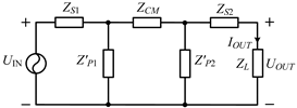
Constant Current Input
Electronics 12 00245 i002
CC
Output
Condition Z 12 2 Z 11 Z 22 = 0 Z P 1 + Z S 1 / / ( Z C M + Z P 2 ) = 0 Z 22 = 0 Z P 1 + Z C M + Z P 2 = 0
Output Gain I O U T = U I N Z 12 Z 11 Z 23 G I = | I O U T I I N | = | Z P 1 Z P 2 | = | Z 12 Z 23 |
Input Impedance Z I N = Z 11 Z 23 2 Z 23 2 Z 22 Z 33 Z I N = Z 11 + G I 2 Z 33
CV OutputCondition { Z S 1 + Z P 1 = 0 Z S 2 + Z P 2 = 0 Z 23 2 ( Z 33 Z L ) Z 22 = 0 Z P 2 + Z S 2 / / ( Z C M + Z P 1 ) = 0
Output Gain U O U T = U I N Z 12 Z 23 Z 12 2 Z 11 Z 22 U O U T = Z P 1 ( Z S 2 + Z P 2 ) Z P 2 I I N
Input Impedance Z I N = Z 11 + Z 33 Z 12 2 Z 23 2 Z 22 Z 33 Z I N = Z P 1 2 ( Z S 2 + Z P 2 ) Z L Z 22 + Z S 1 + Z P 1 ( Z C M + Z P 2 ) Z 22
Table 2. Comparison of SP-based compensation topologies to achieve CC output.
Compensation TopologiesCC Output
ConditionsOutput Current
Electronics 12 00245 i003
Double-sided LC compensation topology
ω 2 L S 1 = C P 2 + C M C P 1 C P 2 + C P 1 C M + C P 2 C M I O U T = j ω C P 1 C P 2 + C P 1 C M + C P 2 C M C M U I N
Where
C P 1 = C P 1 + C e 1 , C P 2 = C P 2 + C e 2
ZPA can be achieved with the condition:
ω 2 L S 2 = C P 1 + C M C P 1 C P 2 + C P 1 C M + C P 2 C M
Electronics 12 00245 i004
Double-sided CL compensation topology
{ ω 2 L P 1 = C e 2 C S 1 C e 2 + C e 1 C e 2 + C e 1 C M + C e 2 C M ω 2 L P 2 = C e 1 C e 1 C e 2 + C e 1 C M + C e 2 C M
ZPA can be achieved with the condition:
C S 2 = C b 2 C c + C b
Z I N = L P 2 C b Z L
I O U T = j ω C S 1 C e 2 C e 1 U I N
Where { C b = C e 1 C e 2 + C e 1 C M + C e 2 C M C e 1 C c = C e 1 C e 2 + C e 1 C M + C e 2 C M C M
Electronics 12 00245 i005
CL−LC compensation topology
ω 2 L P 1 = ( 1 C a + 1 C c ) 1 C S 1 1 C a + 1 C c + 1 C S 1 I O U T = j ω ( 1 + C c C a ) U I N
Where { C a = C e 1 C P 2 + C e 1 C M + C P 2 C M C P 2 C b = C e 1 C P 2 + C e 1 C M + C P 2 C M C e 1 C c = C e 1 C P 2 + C e 1 C M + C P 2 C M C M
and CP2 = CP2 + Ce2
ZPA can be achieved with the condition:
ω 2 L S 2 = 1 C b + 1 C c C a C c C a + C c ( 1 + C a C c ( C a + C c ) C S 1 )
Z I N = C a C c Z L C S 1 ( C a + C c )
Electronics 12 00245 i006
LC−CL compensation topology
{ ω 2 L S 1 = 1 C a ω 2 L P 2 = 1 C b I O U T = j U I N ω L P 2
Where { C a = C P 1 C e 2 + C P 1 C M + C e 2 C M C e 2 C b = C P 1 C e 2 + C P 1 C M + C e 2 C M C P 1 C c = C P 1 C e 2 + C P 1 C M + C e 2 C M C M
and CP1 = CP1 + Ce1
ZPA can be achieved with the condition:
C S 2 = C b 2 C b + C c
Z I N = 1 ( ω C b ) 2 Z L
Table 3. Comparison of SP-based compensation topologies to achieve CV output.
Compensation TopologiesCV Output
ConditionsVoltage Gain
Electronics 12 00245 i007
Double-sided LC compensation topology
{ ω 2 L S 1 = 1 C P 1 + C e 1 ω 2 L S 2 = 1 C P 2 + C e 2 G V = C P 1 + C e 1 C P 2 + C e 2
Where
CP1 = CP1 + Ce1, CP2 = CP2 + Ce2
ZPA cannot be achieved
Z I N = 1 G V 2 / Z L j ω C P 1 ( C P 1 / C M + C P 1 / C P 2 + 1 )
Electronics 12 00245 i008
Double-sided CL compensation topology
{ ω 2 L P 1 = C e 2 C S 1 C e 2 + C e 1 C e 2 + C e 1 C M + C e 2 C M ω 2 L P 2 = C e 1 C S 1 C e 1 + C e 1 C e 2 + C e 1 C M + C e 2 C M G V = C S 1 C e 2 C S 2 C e 1
Where
{ C a = C e 1 C e 2 + C e 1 C M + C e 2 C M C e 2 C b = C e 1 C e 2 + C e 1 C M + C e 2 C M C e 1 C c = C e 1 C e 2 + C e 1 C M + C e 2 C M C M
ZPA cannot be achieved
Z I N = 1 / ω 2 C S 1 2 1 + ( C e 2 C e 1 ) 2 ( 1 1 ω 2 C S 2 2 Z L ) j C c ω C a 2
Electronics 12 00245 i009
CL−LC compensation topology
{ ω 2 L P 1 = 1 C S 1 = 1 C a + 1 C c ω 2 L S 2 = 1 C b + 1 C c G V = C S 1 C c
Where
{ C a = C e 1 C P 2 + C e 1 C M + C P 2 C M C P 2 C b = C e 1 C P 2 + C e 1 C M + C P 2 C M C e 1 C c = C e 1 C P 2 + C e 1 C M + C P 2 C M C M
and CP2 = CP2 + Ce2
ZPA can be achieved
Z I N = ω 4 C c 2 L P 1 2 Z L
Electronics 12 00245 i010
LC−CL compensation topology
{ ω 2 L S 1 = 1 C a + 1 C c ω 2 L P 2 = 1 C S 2 G V = C c C S 2
Where
{ C a = C e 1 C P 2 + C e 1 C M + C P 2 C M C P 2 C b = C e 1 C P 2 + C e 1 C M + C P 2 C M C e 1 C c = C e 1 C P 2 + C e 1 C M + C P 2 C M C M
and CP2 = CP2 + Ce2
ZPA can be achieved with the condition:
{ ω 2 L P 2 = 1 C b + 1 C c Z I N = Z L ω 4 C c 2 L P 2 2
Table 4. Circuit Models Of Capacitor And Inductor With Parasitic Resistance.
CapacitorInductor
Circuit modelElectronics 12 00245 i011Electronics 12 00245 i012Electronics 12 00245 i013Electronics 12 00245 i014
Parasitic resistancerCS = 1/(ωC · QC)rCP = QC/(ωC)rLS = (ωL)/QLrLP = ωL · QL
Table 5. Experimental Parameters.
SymbolValue
Udc/V20
RL100
f/MHz1
CM/pF114.8
CP1/nF1
CS2/pF202.1
LS1H25.28
LP2H125.3
Disclaimer/Publisher’s Note: The statements, opinions and data contained in all publications are solely those of the individual author(s) and contributor(s) and not of MDPI and/or the editor(s). MDPI and/or the editor(s) disclaim responsibility for any injury to people or property resulting from any ideas, methods, instructions or products referred to in the content.

