Article

Gamma Ray Effects on Multi-Colored Commercial Light-Emitting Diodes at MGy Level

1
Laboratoire Hubert Curien, UMR-CNRS 5516, Université Jean Monnet, F-42000 Saint-Etienne, France
2
CEA, DAM, DIF, F-91297 Arpajon, France
3
CEA, DAM, CEG, F-46500 Gramat, France
*
Authors to whom correspondence should be addressed.
Electronics 2023, 12(1), 81; https://doi.org/10.3390/electronics12010081
Submission received: 1 December 2022 / Revised: 18 December 2022 / Accepted: 21 December 2022 / Published: 25 December 2022
(This article belongs to the Special Issue Radiation Tolerant Electronics, Volume III)

Abstract

:
Light-emitting diodes (LEDs) are of interest for implementation in radiation environments, such as part of illumination systems of radiation-tolerant cameras able to provide images at high doses (>MGy). It is then mandatory to characterize the radiation effects on all of the LED key properties exploited for such applications. To this aim, the evolution of the optical properties of commercial LEDs after they have been exposed to γ-rays, up to total ionizing dose (TID) levels of 2 MGy(air) at room temperature, is discussed. The devices under test include four LEDs of different colors (red, green, blue and white) in the same package. This allows a direct comparison between the responses of the different structures and technologies, as the proximity between the diodes ensures the uniformity of their irradiation conditions. The radiation effect on the electron–photon conversion mechanisms inside these LEDs is investigated through the evolution of their external quantum efficiency (EQE) vs. current characteristics. The spectral emission pattern of LEDs after irradiation at different dose levels is then characterized to estimate the TID effects on the lens which surrounds the LED package. The presented results show a monotone radiation-induced EQE decrease as a function of the TID, especially in the red LEDs. For the tested red LEDs, the EQE decreased up to 78% after a TID of 1 MGy when they were OFF during irradiation, and up to 8% when they were ON during irradiation. A visual inspection of the devices after irradiation shows a mechanical degradation of the lens shared among the four diodes. However, the emission pattern analysis does not show any significant radiation-induced changes in the optical properties of the lens. Based on these results, it appears possible to design LED-based illumination systems able to survive to MGy dose levels that can be integrated as subsystems of radiation-hardened cameras.

1. Introduction

Light-emitting diodes (LEDs) are steadily substituting halogen and fluorescent light sources in many applications thanks to their high efficiency, long life cycle, fast switch time, mechanical robustness and small form factor [1,2]. For the same reasons, LEDs are being increasingly used in radiation-harsh environments. The successful implementation of LEDs in these environments can solve many of the well-known and tight constraints which usually characterize them. The space environment is an example of this type of application, as dimensional and power constraints are among the most critical factors for the implementation of any solution designed to be launched in orbit [3,4,5]. High-energy facilities include lighting solutions that are being designed to take advantage of LEDs as well. The main reason remains the tighter energetic requirements for these structures in recent years, pushing the implementation of more energy-saving lighting solutions. As an example, one of the proposed solutions to save energy consists of taking advantage of the really low on/off switch time and how easy they are to control to turn them on only when necessary [6,7].
As another case study in which LEDs are increasingly gaining popularity, efforts are made to develop radiation-hardened cameras able to provide imaging solutions in radiation-rich environments [8]. Such solutions require the ability to conceive CMOS image sensors, optical systems and illumination systems able to survive in these hostile environments while maintaining the image quality at a sufficient level despite the radiation impact of each subpart of the camera.
Nowadays, it has been demonstrated that CMOS image sensors (CISs) can be designed to resist MGy dose levels, with pixel architecture exhibiting a low dark current increase after exposure to X- or γ-rays [9] and marginal changes in their quantum efficiencies. Similarly, it was shown that monochrome or color optical systems can be conceived using either radiation-hardened optical glasses or even using commercial glasses that present limited darkening at such dose levels [10,11]. Both subsystems’ degradation mechanisms affect the photometry budget of the camera resulting in a degradation of the signal to noise ratio of the camera. LEDs are known to exhibit a good radiation tolerance to ionizing radiations, at least at moderate total ionizing doses (TIDs), and a larger vulnerability against displacement damages [12,13,14]. In particular, their output power has been observed to decrease under irradiation, reducing the number of photons reaching the detector and accordingly degrading the image quality. In most cases, LEDs can continue to function even after exposure to the TID, although they may exhibit some performance degradation [15].
As discussed in [16], multiple factors are in need of being assessed and qualified for the lighting solution in a rad-hard camera system. It is not only the global output power of the LEDs which is crucial to controlling and predicting the photometry budget of the camera system. It is also the angular dependence of the photon emission that determines the number of photons capable of reaching the object of interest and traveling back up to the image sensor.
The emission spectra that can control the imaging colorimetry aspect should be considered as well. Another important aspect to consider for a camera system is the compensation of radiation damages of one part of the subpart of the camera to another one. In particular, if the degradation of the CMOS image sensor and of the optical system are difficult to mitigate by acting at the system level, it might be possible to design an LED-based illumination system able to compensate for part of the camera degradation by having some margin in the optical powers that LEDs can provide or by having additional LEDs that can be activated [17]. This paper focuses on commercially available LEDs and includes a comparison of different LED technologies in terms of their radiation hardness. This is a unique aspect compared to previous works such as the one by Allanche et al. [17], which focused on the study of the radiation resistance of high-power white LEDs.
In this context, and to further advance lighting system development for high-TID environments, this article investigates the permanent gamma radiation effects on several key aspects of commercially available LED properties: the decrease in their efficiency at different injection currents with TIDs for different LED technologies, the evolution of their emission spectra and emission patterns with dose and the dependence of their radiation response regarding their profile of use, either ON or OFF during the γ-rays exposure. Results of visual inspection and qualitative considerations on the mechanical degradation of some of the materials composing the LED are reported. These results can be directly used to design radiation-hardened lighting systems for operation in harsh environments, as well as for the design and performance optimization of high-dose radiation-tolerant cameras.

2. Materials and Methods

2.1. Tested LEDs

The effects of ionizing radiation on 13 commercial Cree XML Color LEDs have been investigated [18]. Each LED includes four different diodes in the following colors: red, green, blue and white. Each color can be individually controlled, allowing for a more accurate control of the colorimetry aspect of the imaging solution. The parallel use of these four LEDs allows the combination of two different techniques normally used to create white LEDs to create a ‘super white’ LED. The first technique consists of combining a blue (in certain cases ultraviolet, UV) LED with a phosphor layer to create a white LED (almost-white spectrum) through the phosphor’s yellow luminescence. The second technique consists of the simultaneous use of a red, a green and a blue LED [1,2]. In the investigated devices, the first technique has been used to include a white-colored LED together with the other three colors. From the datasheet [18] and from the spectral intensity results, it can be concluded that the white LED and the blue LED share the same structure, the only difference being the phosphor layer on top of the white one.
Figure 1 shows the structure of the four LEDs of the tested devices, embedded at the center of a plano-convex lens to redirect the emitted light and obtain a Lambertian emission pattern with a viewing angle of 130° [18].
The tested components are commercial devices, usually referred to as components off the shelves (COTS). Accordingly, limited information on the LED composition and structure is available [18]. The results collected in the present work allowed further information of the LED composition/structure to be collected, in addition to the information already contained in the datasheet.
The luminous spectrum emitted by an LED depends on the energetic bandgap resulting from the combination of layers of semiconductor materials inside the PN junction, together with the presence of single or multiple quantum wells or cavities inside the structure. Depending on the used materials, and based on their emitted spectral range, LEDs can be divided into two categories. The first category is for the colors from the UV up to amber (200–620 nm), which are based on GaN technologies, while the second one is for wavelengths above 620 nm, from red to infrared, which are based on AlGaInP structures [1]. Concerning the devices investigated in this work, the white, blue and green LEDs can be placed in the first category, and the red one in the second one.

2.2. Irradiation Conditions and Investigated Samples

Passive irradiation of the samples was carried out over two irradiation campaigns at the IRMA (IRradiation MAtériaux) facility at the Institute de Radioprotection et de Sûreté Nucléaire (IRSN, Paris, France) [20] with a Co60 gamma ray source (two peaks at 1.17 and 1.33 MeV). At this facility, it is possible to control the dose rate at which the sample is exposed to by changing the distance between the sample and the Co60 source. During the first irradiation campaign, which lasted for ~21 days, 2 sets of 4 samples were irradiated at two dose rates: 990 Gy/h and 1990 Gy/h, up to a final dose of ~500 kGy and ~1 MGy, respectively. In this paper, all of the dose quantities are expressed in Gy(air).
For the second irradiation campaign, which lasted for 25 days, 8 samples were chosen among which 5 had been irradiated in the first campaign and 3 were pristine. Two of these samples were irradiated at 833 Gy/h, being exposed to a total dose of about ~500 kGy. The other 6 samples were exposed to a dose rate of 1590 Gy/h, reaching a final dose value of 1 MGy.
Table 1 reports all the investigated samples and the TID levels that they were exposed to in the first and second irradiation runs, together with the final TID. The ‘Performed analysis’ column reports which one of the two analyses was implemented to study the sample. ‘EQE’ refers to the external quantum efficiency study presented in Section 2.3. and ‘Pattern’ refers to the radiation pattern study described in Section 2.4. NP1 and NP2 refer to two non-irradiated samples coming from a new acquired batch of LEDs which were included in the radiation pattern analysis. One of the LEDs, referred to as P3, was kept ON during irradiation, while all the others were in the OFF state.

2.3. External Quantum Efficiency

The figure of merit (FoM) describing the total efficiency of an LED is the external quantum efficiency (EQE) [1]. This quantity includes information about the inefficiencies introduced by all of the different factors in the conversion process from the electrons fed to the contacts of the junction to the photons which exit the optics of the device. It is defined as:
EQE = ϕ p h ϕ e l = η e x t × IQE
where   ϕ p h is the flux of photons emitted by the LED per second, ϕ e l is the flux of electrons injected into the LED per second, η e x t is the extraction efficiency and IQE is the internal quantum efficiency.
The effects of the different parts composing the structure of an LED on its EQE can be divided into two contributions, IQE and η e x t , depending on the type of inefficiency that they introduce. IQE describes the efficiency of the electron-to-photon conversion inside the PN junction. It accounts for two effects: radiative recombination efficiency and amplification (if present, as in the case of laser diodes).
η e x t includes the effects of the optical components designed to extract and diffuse the photons generated by the PN junction. It considers contributions associated with lenses, extraction patterns (if present) and phosphor layers (for white LEDs).
The EQE characteristic is current dependent, and can be represented in the well-known bell shape. This bell shape can be explained considering the competition among the different types of electron–hole recombination inside the junction, and can be retraced back to the IQE vs. current characteristic. Using a simplified approach, the IQE can be described considering three main recombination mechanisms: Shockley–Read–Hall (SRH) recombination, also known as trap-assisted recombination, which dominates the low current section of the curve; radiative recombination (the useful one for LEDs), dominating the region around the maximum IQE value and Auger recombination, which is thought to be the main actor in the efficiency droop mechanism responsible for the efficiency decrease observed at high currents.
The efficiency droop effect has been mainly documented for GaN devices. Many recent studies have been devoted to the explanation of this effect by introducing additional phenomena, such as an increased current leak [21,22]. This work does not consider these additional effects, as previous studies [10,17] have shown that the exposure of LEDs to ionizing radiation mostly impacts the low current region of their IQE curves.
This phenomenon is explained in the literature by a radiation-induced increase in the number of traps inside the LED, which increases the probability of SRH non-radiative recombination and, consequently, reduces the probability of radiative recombination in low injection current regimes [1,23].

EQE Characterization: Setup

To investigate the EQE as a function of the LED-injected current curve, the setup shown in Figure 2 has been implemented. It includes a Labsphere Ltd. LCS-100 integrating sphere system, implementing a Labsphere CDS-600 spectrometer [24] and an Agilent AE3646A source meter unit (SMU) [25]. The integrating sphere is composed of a reflective spherical surface of 25.4 cm in diameter in which the sample is placed. On the side of the sphere, there is an opening connected to an optical fiber (OF) which is connected to a spectrometer.
This configuration allows the intensity emitted by the sample to be measured, integrating it over all directions. The system response is calibrated before the sample measurement with two halogen sources (Labsphere SCL-600 and AUX-600 [24]) to obtain the spectral intensity, expressed in W per nm. The inclusion of an SMU allowed the LEDs to be driven at specific currents while monitoring the necessary voltage in real time.
Each color of each sample has been characterized using a stepped process over seventeen injected current values ranging between 0.5 mA and 1 A. At each current value, the LED was kept ON for one minute and then turned OFF for another minute before the next step, to reduce the effects of self-heating. The temperature outside of the sphere was monitored during the test. It remained between 22 °C and 25 °C.
The results reported in this paper describe the EQE investigation of the available samples (P1, P2 and P3) irradiated only during the second irradiation run.
These samples were characterized by the described setup before and after the second irradiation run. As seen in Table 1, the P1 sample was irradiated at 500 kGy TID. The P2 and P3 samples were irradiated at 1 MGy. The four LEDs of the P3 sample were biased with a 0.1 A current (for a 0.4 A total current) throughout the whole irradiation.

2.4. Radiation Pattern Study

To investigate the radiation effects on the LED extraction efficiency η e x t , a dedicated setup was used to characterize the emitted radiation pattern of our samples. The setup illustrated in Figure 3 was used to measure the emitted spectrum of a sample biased at 0.1 A, one color at a time. The LED was rotated around its vertical axis across angles between −90° and 90° from the perpendicular direction of its die. An angular resolution of 3° per step was used. Thirteen samples were characterized with two full scans (from −90° to 90° and back) to remove possible noise contribution coming from external factors, such as stray reflections and transient light sources.
To measure the emitted intensity at different angles, an OF was placed in front of the LED at a distance of 35 cm and connected to a spectrometer ([26]). It was decided to rotate the sample on its axis, instead of having the OF rotating around the sample, to minimize the influence of the OF transmission characteristics on the measured spectra. Indeed, the bending of the OF caused by its movements can change the transmission spectrum seen from the spectrometer, compromising the quality of results.
This setup provides a matrix of spectra at different angles per sample, so for different TIDs. Results are reported in the two types of graphs of Figure 4. The investigation of the spectral intensity dependence on the emitted angle, as shown in Figure 4a, provides information on the primary optics of our LEDs, where in our case the primary optics are composed of the hemispherical lens in which the sample is encapsulated. The measured spectra can then be integrated to evaluate the emitted optical power in each direction, to characterize a polar emission pattern (see 
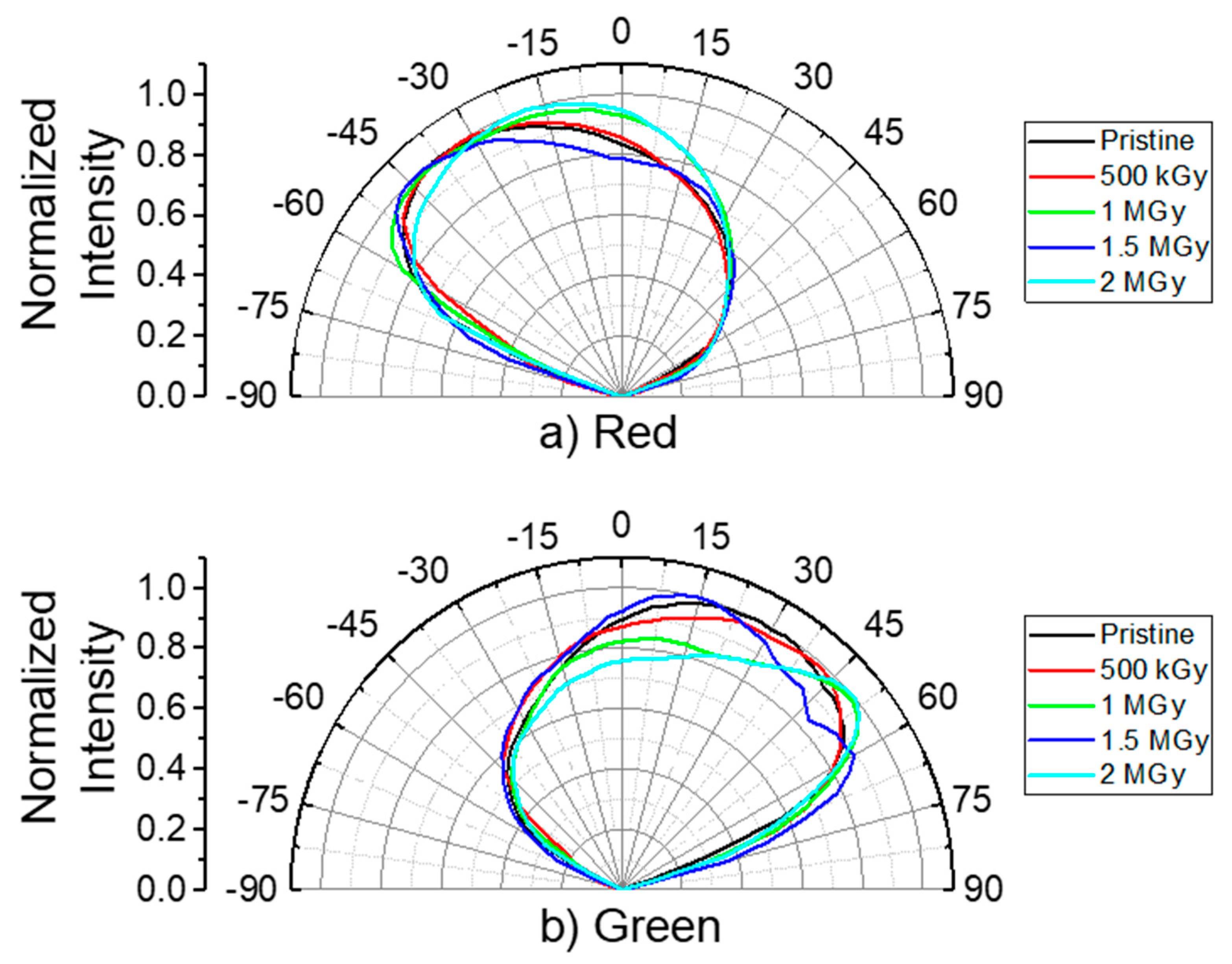
Figure 4b). This allows the effects of gamma radiation on the optical power emitted at each investigated angle to be investigated. These spectral measurements are not calibrated such as the ones acquired with the integrating sphere; then, all the results are normalized around the angle with the maximum measured intensity.
Figure 4a reports the measured spectra of a pristine white LED (NP1) at different angles normalized at the center of the blue band (~440 nm). This figure highlights the spectral changes as a function of the angle. This is caused by the chromatic dispersion of light inside the lens. The different positions of the LEDs inside the package result in an emission pattern such as the one shown in Figure 4b. This disposition allows the lights emitted by the different LEDs to be combined when all are turned ON at the same time to obtain the aforementioned super-white spectrum.

3. Results

3.1. LED Visual Inspection

The lens, which is shared by the four diodes composing a single LED, is a transparent semi-sphere of unknown material. From visual inspection and handling, the lenses of the unirradiated LEDs seem soft and rubbery, suggesting that they could be made of optical-grade silicone [1], as this can be recognized for its elastic properties. Non-metallic materials are generally subjected to several types of radiation-induced effects. At the macroscopic level, irradiated commercial components can experience structure softening or hardening, along with other visible effects such as color change and, in particular, darkening [27]. Severe radiation-induced degradations are reported to occur in commercial polymeric materials at doses in the MGy range, in some cases leading to the component’s structural failure and possibly compromising the operation of the whole system that they are a part of.
Figure 5 shows four pictures of some tested samples, where the position of the four diodes and their color distribution are visible. The distribution corresponds to the one reported in Figure 1. The red LED is located in the top left position, while in the bottom left we can recognize the white LED thanks to the presence of the yellow phosphor layer. The green and blue LEDs are located in the top right and bottom right positions, respectively, as shown in Figure 5b. From this picture, it is also visible that most of the light emitted from a single diode is transmitted toward the opposite side of the hemispherical lens with respect to its position inside the lens. This explains the apparent position change between the pictures in Figure 5a,b, as the red LED, positioned in the top left corner, emits part of its light toward the lower right side of the picture because of light reflection inside the lens. The other LEDs behave in the same way, resulting in the color distribution observed in Figure 5b.
Figure 5c,d illustrate the radiation-induced degradation of the LED structure at 1 MGy and 2 Mgy of dose, respectively. The two main macroscopic modifications of the materials composing the LED are highlighted. First, a radiation-induced darkening of the surface above the reflective layers surrounding the LED die is clearly visible. The surface color of the non-irradiated sample (Figure 5a) is white-ish, while it becomes progressively darker and brown-ish with dose, as shown in Figure 5c,d.
Additionally, mechanical damages on the lens structure can be observed. They are particularly severe after irradiation at 2 MGy, and they appear in the form of the nicks and scratches visible above the four diodes. These damages might compromise the optical properties of the lens. For example, the diodes’ details in Figure 5d appear blurred and distorted in comparison to those observed in the non-irradiated sample. From handling, the lenses of all the LEDs irradiated at 1 MGy and 2 MGy appear hardened by radiation. The soft appearance and the elastic properties of the non-irradiated lens are compromised by radiation and permanently lost. The structural damage reported in some of the irradiated lenses probably originates from the post-irradiation handling and shipment. During these phases, the samples might have been accidentally exposed to unforeseen mechanical stresses, such as ones caused by uncontrolled impacts, leading to a permanent fracture of some of the lenses fragilized by radiation.
Finally, it has been attempted to mechanically remove the lens to perform additional tests on the four LEDs without it. However, since the lens has been deposited over the contacts to provide the mechanical strength to keep them in place, its removal resulted in the rupture of the contacts, making the diodes unusable. This structural behavior of the lens is compatible with the hypothesis for which the lens is made out of silicone, as silicone is often used for the construction of LED lenses due to its flexibility [1].
Figure 6 shows some severe examples of LEDs’ mechanical degradation. Part of the lens is missing in sample I05M1, irradiated at 1.5 MGy (left picture), and the lens is badly damaged in several places in sample I1M2, irradiated at 2 MGy (right picture). A mechanical damage to the lenses is clearly visible from these pictures. This damage probably originated during the transport of the samples to the irradiation facility for the two runs or during their post-irradiation handling. The damage is not uniform over the lens volume. Concerning the 1.5 MGy sample (Figure 6, left), the structural failure of the lens is more evident in the top sector of the device, and in particular with regards to the green LED.

3.2. External Quantum Efficiency

The EQE curves of P1, P2 and P3 samples and their variation as a function of the dose are investigated. Figure 7 shows the EQE curve for the P3 sample before and after irradiation as an example. The typical EQE bell shape on both pristine and irradiated curves can be recognized.

3.2.1. Radiation-Induced Efficiency Change

As the representation of the EQE vs current characteristics for all the samples and colors before and after irradiation can become hard to read (as seen in Figure 7) due to the quantity of curves in a single figure, a FoM referred to as a radiation-induced efficiency change (RIEC) has been used. It is defined as:
RIEC = EQE Irradiated EQE Pristine  
This quantity describes the variation in EQE at different currents as a function of the absorbed dose, allowing a direct comparison between the curves of different samples.
Figure 8 reports the RIEC characteristic of P1, P2 and P3 samples divided by color. The EQE degradation of samples P1 and P2, which were OFF during irradiation, can be appreciated. It is more pronounced at lower currents, as expected from the literature [17]. This effect is much more evident for the red LEDs, as an efficiency decrease of up to 78% can be observed at lower currents. For all the other colors, a lower degradation is observed, corresponding to EQE variations of 20–25%, but it still affects the low current region of the graphs more.
Very different results are reported for the P3 sample, which was kept ON for the whole irradiation run at 0.1 A per diode. The decrease in the blue and white LEDs is almost flat across the whole current range (~10% for both), whereas EQE at low currents of the green LED increases with dose, even exceeding the pristine level. In the red LED curve, the degradation at low currents seen in the other two samples is still appreciable, but more limited, not exceeding 10% variation.

3.2.2. Spectral Flux Characterization

To further analyze the results presented in the previous section, the spectral response of each LED before and after irradiation has been analyzed, to investigate whether the previous results can be explained by a variation in the emitted spectrum shape related to the TID. Figure 9 reports graphs of the measured spectral fluxes of the four diodes individually driven at 0.1 A.
The degradation of the spectral flux of the red LED as a function of the dose can be observed in both Figure 9a,b. No evident modification in the associated spectral shapes is reported. In Figure 9b,c, a decrease in the measured intensity of both the blue and white LED is clearly visible, while the shape of the flux remains the same. Since these two LEDs share the same structure, apart from the phosphor layer present on top of the white one, a similar evolution of the spectral flux as a function of the dose seems reasonable. This decrease is present in the yellow band of the spectrum as well. However, this is not obvious from the figure, as it spreads across a larger wavelength span. None of the curves reported in Figure 9 show any appreciable change in the shape of the measured emitted spectra of the samples after irradiation.

3.3. Radiation Pattern Study

The graphs reported in Figure 10 show the intensity radiation patterns of eleven of the measured samples normalized to the maximum measured intensity, divided by color. Two samples, marked as damaged in Table 1, were excluded from this analysis as they showed very different radiation patterns. These two samples are further discussed in Section 3.3.1. The presented curves were obtained by averaging the measured radiation patterns of all the samples exposed at the same TID. These results introduce a qualitative analysis of the effects of the TID on the Lambertian emission pattern of the LEDs.
The curves have been averaged over different numbers of samples, depending on the actual number of devices irradiated up to a specific TID. As described in Table 1, the pristine and 500 kGy curves are averaged over the measurements of two samples each. The 1 MGy curves are averaged over five samples which reached this dose in different conditions. The 1.5 MGy and 2 MGy curves show the response of a single sample each, as the second sample of each of these doses had been damaged and is discussed in the next section. It is worth mentioning that the emission patterns for the P3 sample, which was biased during its exposure to γ-rays, did not show any different behavior from the other samples irradiated up to 1 MGy, which justifies its inclusion in the average curve for this dose in Figure 10.
Concerning the white and blue LED, the shape of the polar radiation patterns show very little variation as a function of the dose up to 1.5 MGy. This variation does not show any specific trend. Concerning the green and red LEDs, similar considerations apply up to 500 kGy.
By contrast, changes in the shape of the irradiation pattern are reported at higher doses. In particular, the 2 MGy curves for the white and blue LEDs show an enlargement of the radiation pattern, which spreads over a wider angle range.
In Figure 10b, it is possible to see a structured pattern for the green LED, as the 1 MGy and 2 MGy curves similarly diverge from the pristine one, with the peak intensity shifted toward the right. However, the 1.5 MGy curve is flatter.
Figure 10a shows that the 1 MGy and 2 MGy radiation patterns are similar for the red LED, but without any evident change in direction in the intensity peak. Instead, they show an enlargement of the pattern similar to the one seen for the blue and white LEDs. The 1.5 MGy curve shows a different radiation pattern, deviated toward the left. It is recalled that the four LEDs share the same lens, meaning that any radiation-induced effect on the silicone lens should equally affect all the four characteristics curves, as in the tested irradiation conditions a uniform exposition of the whole package was ensured.

3.3.1. Radiation Pattern for the Damaged Samples

Figure 11 reports the emission polar pattern for the two samples reporting severe lens damage shown in Figure 6. Because of the relevant modification in the lens structure, the measured radiation pattern completely differs from the other samples.
It is indeed possible to correlate the changes in the radiation pattern shown in Figure 11b for the green LEDs with the big damages shown in Figure 6. In fact, the portion of the lens most affected by structural degradation is located above the green LED, which in the pictures is in the top right position. It is indeed the LED where the radiation pattern is most affected. From the red LED polar pattern of the I05M1 sample, it is possible to recognize the part where the portion of the lens is missing from the low normalized intensity observed at angles below −15°. From the white and blue LEDs (Figure 11c,d), it is possible to relate the anomalies in the radiation pattern with a damaged part of the lens common for these colors, preventing part of the LEDs’ light to be transmitted. This damage can be recognized in Figure 6 in the central area between the white and blue LEDs, on the bottom part of the package.

4. Discussion

The visual inspection of the LED package at different TIDs provides evidence for a darkening of the area around the lenses. Additionally, a progressive increase in the damages on the lens structure with dose is observed. These mechanical damages are not uniformly distributed across the lens volume, and are most likely an effect of the post-irradiation handling of the LEDs. In fact, additional mechanical stresses might originate from accidental impacts occurred during the transport to and from the irradiation facility and during the post-irradiation characterization. In particular, the samples irradiated in both irradiation runs traveled twice to and from the facility, increasing the risk of mechanical stresses. The damage entity seems to increase with the dose, suggesting that radiation influenced the elastic properties of the silicone lens, reducing its capability to absorb mechanical stresses, such as the ones originating from accidental and uncontrolled impacts, and making it more fragile and so more susceptible to structural failure.
Apart from the samples described in Figure 6 and Figure 11, in which the degradation of the optical properties is evident, it is generally difficult to quantify the impact of the mechanical damages on the optical properties of the LEDs. In fact, no damage-dependent behavior can be recognized in the intensity radiation patterns of Figure 10 up to 1.5 MGy. The widening of the intensity patterns in the 2 MGy curves of all colors in Figure 10 could indicate the presence of scattering-inducing defects inside of the lens related to the gamma ray-induced displacement damage, which is also coherent with the blurring of the lens observed in Figure 5d. Considering the results from the visual inspection, and taking into account that the four diodes composing an LED share a common lens, the observed shape variations (especially in the green LED’s response) can be associated with a lens mechanical damage as they clearly do not affect the emission pattern response in the same way for the four colors.
Figure 8 shows that the decrease in the EQE is mostly concentrated at low injection currents for all of the diodes of the samples irradiated in their OFF state, P1 and P2. This region of the EQE vs. the current characteristic is dominated by SRH non-radiative recombination, also called trap-assisted recombination [1,28]. This information supports the hypothesis that gamma radiation promotes the generation of new traps inside the LED die. The efficiency variation at low currents has already been documented and attributed to the presence of trap states, such as traps present on the perimeter of a diode when trying to miniaturize the device, both for GaN [23] devices and InGaP [29,30] devices.
The higher stability of the green LED response reported in Figure 8b in comparison to the other colors can be explained by analyzing the given EQE curve in Figure 7. It is visible that inside the investigated range of currents, the efficiency droop seems to be the dominating mechanism, as the EQE peak is positioned at a much lower current than the other diodes, and the curve decreases as a function of the current.
The blue and the white LEDs have very similar responses in all three samples, with a slight divergence at higher currents. This similarity is expected, as they share the same structure except for the phosphor layer on the white one. It is difficult to attribute the difference between the two LEDs to the phosphor layer with these measurements, as no observable variation in the blue and yellow bands (and their relative intensities) of the white spectra shape is present. A possible explanation for this is that the presence of the phosphor layer slightly changes the thermal response of the diode, increasing the self-heating during the EQE characterization because of the extra layer of material. This can potentially result in an improved annealing effect of the radiation-induced traps.
In the results shown in Figure 8a, the red LEDs are clearly the most impacted by TIDs, as we observe a 75% decrease in efficiency at low currents when irradiated in their OFF state. This increased sensitivity is explained by the implementation of InGaP technologies needed to design red LEDs [1,4], as this technology has been demonstrated to be much more sensitive to radiation-induced displacement damages when compared to the GaN technologies implemented to obtain the shorter wavelength colors [3,31].
In the curves in Figure 8, it can be seen that the results for the LEDs irradiated in their ON state (P3) show a weaker EQE degradation in their response for all colors. To aid the discussion about the P3 sample, an additional test has been performed where an LED package was characterized before and after a period of 25 days with all diodes biased at 0.1 A. The goal was to quantify the possible effect of the aging of the device on the red curves shown in Figure 8. The maximum EQE variation measured in this test across all colors was 2%.
For the P3 sample, the results for the green LED in Figure 8b show a very high RIEC, which, contrary to the OFF case, is higher than 1 at low currents, indicating an improvement in the EQE after irradiation in this zone and a decrease as the observed current increases. This behavior is similarly observed for the white and the blue LEDs, although the RIEC is lower across all currents. The high RIEC value at a lower current observed for these three LEDs can be explained by competition between the radiation-induced trap generation which explains the OFF curves, and the annealing of these traps caused by the current being injected into the device. The nature of this annealing is probably thermal (self-heating). RIEC values higher than 1 observed in the green LED can be explained by a generation-annealing of trap competition inside the device dominated by the second mechanism, up to the point of annealing the traps present in the device before the irradiation. Both of these explanations can be used to describe the current dependence of the RIEC curves for the blue and the white LEDs of the P3 sample. The cause of the observed degradation (~10%) across all of the investigated currents for the blue and the white LEDs is still under investigation, as the deductions and methods used in this work are not sufficient to give a complete interpretation of the effect. The slight difference in the response of the white and blue LEDs could again be explained by the modified thermal behavior of the diode related to the presence of the phosphor layer.
Figure 8a shows a maximum variation of ~8% for the red LED, still with a larger effect at the lower currents. This is in line with the hypothesis of the competition between trap-generating and trap-annealing processes present when the diode is both excited by the injected current and by the external irradiation field.
The results shown in Figure 9 agree with the previous discussion. The spectral intensity measurements show that the decrease in EQE caused by ionizing radiation does not affect the emitted spectrum of the LEDs. Even for the case of white LEDs, no effect of radiation on the phosphor layer band can be observed with the proposed setup.

5. Conclusions

The results presented in this paper evidence the criticality of the design of LEDs to be implemented in high-radiation environments.
The visual investigation section identifies the lens material as a critical aspect of an LED design, to be considered in particular for its deployment in radiation-rich environments. The selection of a silicone lens bears multiple advantages for the packaging of the device, such as thermal stability and a higher threshold for photo-degradation [1]. The results in this work show that the flexibility of the lens material might be severely compromised by a high TID, increasing the risk of critical damages to the lens which can compromise any radiation hardness achieved in the chosen diode technology. However, the impact of this effect on the performances of an illumination system can be easily mitigated at the system level by appropriate protection of the LEDs.
Indeed, the macroscopic radiation effects reported on the reflective layers and on the lenses indicate that the materials constituting the LEDs already start to suffer from severe radiation-induced damage at the investigated doses, ranging between 1 MGy and 2 MGy. The collected results evidence that LEDs should be considered as complex systems made of various components, whose optical and mechanical properties contribute to its operation and to the definition of its lifetime in high-radiation environments.
The results for the EQE variation with the accumulated dose highlight another important criticality in the design of the commercial package under test. Indeed, the implementation of an RGB-based white LED will be strongly impacted in terms of colorimetry because of the response of the different structures of different colored diodes, whereas this aspect seems to be mostly unaffected for single-LED designs of different colors. This supports the implementation of a single phosphor-based white LED as an illumination solution for the design of radiation-hard cameras or, in case a better white is needed, the only addition of an LED to cover the missing band between the blue and yellow band, instead of additional diodes.
The RIEC results bring forward a warning for the utilization of LED sources in radiation environments in different bias regimes (ON or OFF). The main advantage of this technique is that it saves electrical energy. However, it also introduces a trade-off between power consumption and the reliability of the LED. Keeping the device turned ON when exposed to TIDs may reduce degradation, but this also increases power consumption. These results also allow further discussion on the optical budget compensation for camera solutions in radiation environments. While the degradation variation at different bias currents is something that will need further investigation, the results for the EQE characteristics clearly show a lower impact of ionizing radiation on the LED at higher currents, as these high current injection regimes are less affected by the trap-assisted recombination mechanism that seems to dominate the radiation-induced effects in LEDs. This suggests the solution of implementing a lower number of LEDs driven at higher currents to be more appealing in these environments.

Author Contributions

Data curation, L.W.; investigation, L.W.; resources, O.D., M.G. and P.P.; supervision, A.M., A.B., Y.O., E.M. and S.G.; writing—original draft, L.W.; writing—review and editing, R.C., M.F., A.M., T.A., R.P. and S.G. All authors have read and agreed to the published version of the manuscript.

Funding

Part of the results presented in this paper have been obtained in the framework of the EU project RADNEXT, receiving funding from the European Union’s Horizon 2020 research and innovation program, Grant Agreement no. 101008126.

Data Availability Statement

The data presented in this study are available on reasonable request from the corresponding authors.

Conflicts of Interest

The authors declare no conflict of interest.

References

  1. Schubert, E.F. Light-Emitting Diodes, 3rd ed.; Fred Schubert, E.: New York, NY, USA, 2018; ISBN 978-0-9863826-6-6. [Google Scholar]
  2. Crawford, M.H. LEDs for Solid-State Lighting: Performance Challenges and Recent Advances. IEEE J. Select. Topics Quantum Electron. 2009, 15, 1028–1040. [Google Scholar] [CrossRef]
  3. Johnston, A. Radiation Damage of Electronic and Optoelectronic Devices in Space. In Proceedings of the 4th International Workshop on Radiation Effects on Semiconductor Devices for Space Applications, Tsukuba, Japan, 11–13 October 2000. [Google Scholar]
  4. Swift, G.M.; Levanas, G.C.; Ratliff, J.M.; Johnston, A.H. In-Flight Annealing of Displacement Damage in GaAs LEDs: A Galileo Story. IEEE Trans. Nucl. Sci. 2003, 50, 1991–1997. [Google Scholar] [CrossRef]
  5. Jimenez, J.J.; Hernando, C.; Dominguez, J.A.; Alvarez, M. Proton Irradiation of Commercial High Power Light Emitting Diodes for Space Applications. In Proceedings of the 2011 12th European Conference on Radiation and Its Effects on Components and Systems, Sevilla, Spain, 19–23 September 2011; pp. 894–900. [Google Scholar]
  6. Hosaka, Y.; Nishimori, N.; Itoga, T.; Nakazawa, S.; Tanaka, S.; Seno, T.; Kondo, C.; Inagaki, T.; Fukui, T.; Watanabe, T.; et al. Visualization of Light-Emitting Diode Lighting Damage Process in Radiation Environment by an in Situ Measurement. Jpn. J. Appl. Phys. 2022, 61, 076504. [Google Scholar] [CrossRef]
  7. Devine, J.D.; Floriduz, A. Radiation Hardening of LED Luminaires for Accelerator Tunnels. In Proceedings of the 2016 16th European Conference on Radiation and Its Effects on Components and Systems (RADECS), Bremen, Germany, 19–23 September 2016; pp. 1–6. [Google Scholar]
  8. Goiffon, V.; Rolando, S.; Corbiere, F.; Rizzolo, S.; Chabane, A.; Girard, S.; Baer, J.; Estribeau, M.; Magnan, P.; Paillet, P.; et al. Radiation Hardening of Digital Color CMOS Camera-on-a-Chip Building Blocks for Multi-MGy Total Ionizing Dose Environments. IEEE Trans. Nucl. Sci. 2017, 64, 45–53. [Google Scholar] [CrossRef] [Green Version]
  9. Rizzolo, S.; Goiffon, V.; Corbiere, F.; Molina, R.; Chabane, A.; Girard, S.; Paillet, P.; Magnan, P.; Boukenter, A.; Allanche, T.; et al. Radiation Hardness Comparison of CMOS Image Sensor Technologies at High Total Ionizing Dose Levels. IEEE Trans. Nucl. Sci. 2019, 66, 111–119. [Google Scholar] [CrossRef] [Green Version]
  10. Allanche, T.; Paillet, P.; Goiffon, V.; Muller, C.; Van Uffelen, M.; Mont-Casellas, L.; Duhamel, O.; Marcandella, C.; Rizzolo, S.; Magnan, P.; et al. Vulnerability and Hardening Studies of Optical and Illumination Systems at MGy Dose Levels. IEEE Trans. Nucl. Sci. 2018, 65, 132–140. [Google Scholar] [CrossRef] [Green Version]
  11. Allanche, T.; Muller, C.; Paillet, P.; Duhamel, O.; Goiffon, V.; Rousson, J.; Baudu, J.P.; Macé, J.R.; Desjonqueres, H.; Louvet, C.M.; et al. Radiation Vulnerability of Standard and Radiation-Hardened Optical Glasses at MGy Dose: Towards the Design of Tolerant Optical Systems. J. Non Cryst. Solids 2022, 585, 121531. [Google Scholar] [CrossRef]
  12. Johnston, A.H. Radiation Effects in Light-Emitting and Laser Diodes. IEEE Trans. Nucl. Sci. 2003, 50, 689–703. [Google Scholar] [CrossRef]
  13. Floriduz, A.; Devine, J.D. Modelling of Proton Irradiated GaN-Based High-Power White Light-Emitting Diodes. Jpn. J. Appl. Phys. 2018, 57, 080304. [Google Scholar] [CrossRef] [Green Version]
  14. Zhamaldinov, F.F.; Gradoboev, A.V.; Orlova, K.N.; Simonova, A.V. Recovery of LED Emission Power under the Exposure to γ-n-Pulse. J. Phys. Conf. Ser. 2022, 2261, 012005. [Google Scholar] [CrossRef]
  15. Ahn, K.; Ooi, Y.K.; Mirkhosravi, F.; Gallagher, J.; Lintereur, A.; Feezell, D.; Mace, E.K.; Scarpulla, M.A. Differences in Electrical Responses and Recovery of GaN p + n Diodes on Sapphire and Freestanding GaN Subjected to High Dose 60 Co Gamma-Ray Irradiation. J. Appl. Phys. 2021, 129, 245703. [Google Scholar] [CrossRef]
  16. Muller, C.; Allanche, T.; Paillet, P.; Duhamel, O.; Goiffon, V.; Rizzolo, S.; Lépine, T.; Rousson, J.; Baudu, J.-P.; Macé, J.-R.; et al. Investigations of the MGy Dose Level Radiation Effects on the Photometric Budget of a Radiation-Hardened CMOS-Based Camera. Appl. Opt. 2019, 58, 6165. [Google Scholar] [CrossRef] [PubMed]
  17. Allanche, T. Effect of High Radiation Doses (MGy) on Light Emitting Diodes and Optical Glasses. Ph.D. Thesis, University of Lyon, Saint-Etienne, France, 2020. [Google Scholar]
  18. Cree, Inc. Cree XLamp XML Color LEDs. Available online: https://assets.cree-led.com/a/ds/x/XLamp-XML-Color.pdf (accessed on 23 November 2022).
  19. Cree, Inc. Cree XLamp XML Color LEDs Gen2. Available online: https://assets.cree-led.com/a/ds/x/XLamp-XMLDCL.pdf (accessed on 15 November 2022).
  20. IRSN Installation IRMA. 2015. Available online: https://www.irsn.fr/FR/Actualites_presse/Communiques_et_dossiers_de_presse/Documents/IRSN_Installation-IRMA.pdf (accessed on 29 November 2022).
  21. Dai, Q.; Shan, Q.; Cho, J.; Schubert, E.F.; Crawford, M.H.; Koleske, D.D.; Kim, M.-H.; Park, Y. On the Symmetry of Efficiency-versus-Carrier-Concentration Curves in GaInN/GaN Light-Emitting Diodes and Relation to Droop-Causing Mechanisms. Appl. Phys. Lett. 2011, 98, 033506. [Google Scholar] [CrossRef]
  22. Lin, G.-B.; Meyaard, D.; Cho, J.; Fred Schubert, E.; Shim, H.; Sone, C. Analytic Model for the Efficiency Droop in Semiconductors with Asymmetric Carrier-Transport Properties Based on Drift-Induced Reduction of Injection Efficiency. Appl. Phys. Lett. 2012, 100, 161106. [Google Scholar] [CrossRef] [Green Version]
  23. Olivier, F.; Daami, A.; Licitra, C.; Templier, F. Shockley-Read-Hall and Auger Non-Radiative Recombination in GaN Based LEDs: A Size Effect Study. Appl. Phys. Lett. 2017, 111, 022104. [Google Scholar] [CrossRef]
  24. Labsphere, Inc. LED Characterization System LCS-100. Available online: https://sphereoptics.de/wp-content/uploads/2014/03/Labsphere-Light-Measurement-Systems-illumiaPlus6.pdf (accessed on 15 November 2022).
  25. Agilent Agilent E364x Power Supplies Data Sheet. Available online: https://res.cloudinary.com/iwh/image/upload/q_auto,g_center/assets/1/26/Documents/Agilent/E3640A/e3640a_doc_1.pdf (accessed on 28 November 2022).
  26. Ocean Insight Flame High-Performance Spectrometer. Available online: https://www.oceaninsight.com/globalassets/catalog-blocks-and-images/pdfs/flame_product-sheet.pdf (accessed on 28 November 2022).
  27. Beynel, P.; Maier, P.; Schönbacher, H. Compilation of Radiation Damage Test Data: Materials Used around High-Energy Accelerators; CERN: Geneva, Switzerland, 1982. [Google Scholar] [CrossRef]
  28. Karpov, S. ABC-Model for Interpretation of Internal Quantum Efficiency and Its Droop in III-Nitride LEDs: A Review. Opt Quant. Electron. 2015, 47, 1293–1303. [Google Scholar] [CrossRef]
  29. Li, Y.-Y.; Lin, F.-Z.; Chi, K.-L.; Weng, S.-Y.; Lee, G.-Y.; Kuo, H.-C.; Lin, C.-C. Analysis of Size-Dependent Quantum Efficiency in AlGaInP Micro–Light-Emitting Diodes with Consideration for Current Leakage. IEEE Photonics J. 2022, 14, 1–7. [Google Scholar] [CrossRef]
  30. Oh, J.-T.; Lee, S.-Y.; Moon, Y.-T.; Moon, J.H.; Park, S.; Hong, K.Y.; Song, K.Y.; Oh, C.; Shim, J.-I.; Jeong, H.-H.; et al. Light Output Performance of Red AlGaInP-Based Light Emitting Diodes with Different Chip Geometries and Structures. Opt. Express 2018, 26, 11194. [Google Scholar] [CrossRef] [PubMed]
  31. Ukolov, D.S.; Chirkov, N.A.; Mozhaev, R.K.; Pechenkin, A.A. Radiation Hardness Evaluation of LEDs Based on InGaN, GaN and AlInGaP Heterostructures. In Proceedings of the 2019 IEEE 31st International Conference on Microelectronics (MIEL), Nis, Serbia, 16–18 September 2019; pp. 197–200. [Google Scholar]
Figure 1. Structure of the investigated devices, adapted from [19]. All dimensions are in mm.
Electronics 12 00081 g001
Figure 2. Integrating sphere setup (adapted from [17]).
Electronics 12 00081 g002
Figure 3. Top view schematic of our setup to measure the emitted radiation pattern.
Electronics 12 00081 g003
Figure 4. Example of curves obtained using the setup in Figure 3. (a) Normalized spectra of a pristine white LED at different angles. (b) Normalized intensity radiation pattern for a pristine sample. These results were obtained for the sample NP1.
Electronics 12 00081 g004
Figure 5. The LED structure in different conditions. The unirradiated NP1 sample is shown in its OFF (a) and ON (b) state. The LEDs depicted in the two rightmost pictures have been irradiated at the reported doses of 1 MGy (c) and 2 MGy (d). They refer to samples P2 (c) and I1M1 (d).
Electronics 12 00081 g005
Figure 6. Frontal photography of the two damaged samples, where the damage of the lenses is clearly visible. Sample I05M1 (on the left) and sample I1M2 (on the right).
Electronics 12 00081 g006
Figure 7. EQE vs. current example for our P3 sample (pristine (P) and after 1 MGy of absorbed dose). A 0.1 A drive current was applied to each of this sample of four diodes during the whole irradiation run.
Electronics 12 00081 g007
Figure 8. Radiation-induced efficiency change in the P1, P2 and P3 samples, divided by color. Red (a), green (b), white (c) and blue (d).
Electronics 12 00081 g008
Figure 9. Spectral flux before (solid line) and after (dashed line) irradiation for our P1 (a), P2 (b) and P3 (c) samples. The different LED colors are reported in the legend: white (W), blue (B), green (G) and red (R).
Electronics 12 00081 g009
Figure 10. Measured normalized radiation patterns divided by color. The radiation patterns have been averaged between all the samples irradiated at the same dose value.
Electronics 12 00081 g010aElectronics 12 00081 g010b
Figure 11. Polar radiation pattern of the two damaged samples for the four LED colors. Samples I05M1 and I1M2 were irradiated up to TIDs of 1.5 MGy and 2 MGy, respectively.
Electronics 12 00081 g011
Table 1. List of the investigated samples and irradiation characteristics.
SampleDose 1st Run (MGy)Dose 2nd Run (MGy)Total Dose (MGy)Performed AnalysisComments
P100.50.5EQE + Pattern
P2011EQE + Pattern
P3011EQE + PatternON during irradiation
I05M10.511.5PatternDamaged
I05M20.511.5Pattern
I05M30.50.51Pattern
I05M40.500.5Pattern
I1M1112Pattern
I1M2112PatternDamaged
I1M3101Pattern
I1M4101Pattern
NP1000PatternNew batch
NP2000PatternNew batch
Disclaimer/Publisher’s Note: The statements, opinions and data contained in all publications are solely those of the individual author(s) and contributor(s) and not of MDPI and/or the editor(s). MDPI and/or the editor(s) disclaim responsibility for any injury to people or property resulting from any ideas, methods, instructions or products referred to in the content.

