
Drift Resilient Frequency-Based Sensor Interface Architectures with Adaptive Clock Frequency

1
Department of Electrical and Computer Engineering, Addis Ababa Institute of Technology, Addis Ababa University, Addis Ababa 1178, Ethiopia
2
Department of Electrical Engineering, Faculty of Engineering Technology, Katholieke Universiteit Leuven, 3000 Leuven, Belgium
*
Author to whom correspondence should be addressed.
Electronics 2023, 12(13), 2775; https://doi.org/10.3390/electronics12132775
Submission received: 18 May 2023
/
Revised: 14 June 2023
/
Accepted: 19 June 2023
/
Published: 22 June 2023
(This article belongs to the Special Issue Radiation Tolerant Electronics, Volume III)
Abstract
:Maintaining the accuracy of a sensor system across various operating conditions has always been a challenge, especially for those operating in harsh surroundings such as a radiation environment. Concerning frequency-based sensor interfaces, supply voltage drifts and gain shift of the voltage-to-frequency converter (VFC) are critical design issues. These manifest as gain, offset, and linearity errors at the system level and therefore require continuous correction mechanisms. In this paper, dynamic gain and offset error-compensated open-loop frequency-based sensor interface architectures with adaptive clock frequency are proposed, which result in a ratiometric digital output. To address the mismatch issue, two architectures, one with periodic swapping of the VFCs’ inputs and outputs, and the other with the use of a single analog-to-digital converter (ADC) as an analog front end, are developed. The concepts were demonstrated with implementations on a Zynq board (ZYBO). The results of the first architecture showed that for a 25% gain mismatch between the VFCs, the output gain error was reduced from around 7.4% to 0.79% and the offset error was reduced from around 11.8% to 0.01%. Additionally, for the second architecture, a maximum of 0.11% gain error and 0.1% offset error were recorded for an emulated 25% supply drift.
1. Introduction
In the modern world of technology, the role of sensor systems keeps growing from day to day. The sensor market is forecasted to expand more than twofold within the next decade [1]. What comes with this is a need for the design of accurate sensor systems, which are robust against any environmental factors, such as temperature fluctuations, supply voltage variations, or radiation impacts [2,3,4]. Analog sensor readout parts are greatly impacted by these variations unless a compensation algorithm is incorporated with them. Since these variations are time-varying, they require a continuous calibration algorithm to guarantee the required level of accuracy. Frequency-based sensor-to-digital converters are attractive in this regard since they are digital-intensive structures and most of the signal processing can be performed in the digital domain [5]. Concerning robust output values, digital circuits are less prone to process, voltage, and temperature (PVT) variations and total ionizing dose (TID) impacts than their analog counterparts. In this regard, the VFC is the sensitive component that is susceptible to drift [6,7]. The name VFCs is commonly given to special types of voltage-controlled oscillators (VCOs), typically known for their high linearity [8].
The conventional differential architecture is usually adapted to suppress common mode VCO offset drifts due to environmental variations. However, such structures fall short of compensating dynamic gain errors resulting from a temperature drift or supply voltage variation. Besides, a mismatch between the two VCOs will distort the advantage of using a differential architecture by introducing undesired distortions.
In earlier times, variable temperature issues were addressed by extensive calibration procedures involving a temperature sensor [9], which greatly adds to the complexity of the circuit. Phase-locked loop (PLL)-based sensor readout techniques were also demonstrated as a good option to cancel external effects [10,11], since they work on the principle of relative comparison between two VCOs. A closed-loop Wheatstone bridge sensor readout architecture that works on the concept of balancing the bridge was presented in [12], which suppresses possible supply drifts, but its application is limited to half-bridge structures and the accuracy highly depends on the matching between the two VCOs. Since the VCO operates over a small input range in a closed loop architecture, the system gain error due to the VCO drift is automatically reduced [13]. Nevertheless, the gain drift of the involved digital-to-analog converter (DAC) in the loop has a direct impact on the system gain error, and the mismatch between the two VCOs is still an issue. Time-based chopping techniques were used in [14,15] to remove the remaining gain and offset errors due to VCO mismatches. Here, the chopping frequency inflicts some limitations on the maximum sensor bandwidth that can be used.
To address a mismatch issue between the two VCOs in open loop frequency-based sensor-to-digital converters, a dynamic offset cancelation scheme based on a periodic adjustment of the center biasing voltage of one of the VCOs was demonstrated in [16], which successfully mitigated the offset error due to the relative drift of the VCOs. However, this mechanism lacks a way to correct gain error problems that arise.
Ratiometric measurement approaches have been used in the design of sensor interfaces to reduce the gain error at the system output [17,18,19,20,21]. The ratio operation in [17,18] is performed on two digitized values, which requires a digital signal processing module to provide the final output. Two oscillators that are tuned oppositely by a sensor voltage are employed in [19] where a finite state machine (FSM) is designed to derive the output as the ratio of the oscillators’ frequencies. Here, any relative drift in the oscillators’ gain values will deteriorate the output gain error. A time-based sensor interface where the two outputs of a differential sensor modulate the delay of two halves of an oscillator oppositely was presented in [20,21]; in effect, a pulse-width-modulated (PWM) signal output was generated whose duty cycle is proportional to the sensor value. By using such a relative measurement method, the output can be made independent of the supply and temperature variations. However, this requires the two halves to be closely matched at all times, which would be unlikely if operating in radiation environments.
This paper proposes two open-loop frequency-based sensor interfaces with adaptive sampling clock frequency and mismatch compensation architectures to compensate for any gain and offset errors caused by the drift of environmentally sensitive parameters. The organization of the paper is as follows. In Section 2, the derivation of the adaptive clock and its application in Wheatstone bridge interfacing is demonstrated. Two mismatch-suppressing architectures are then illustrated in Section 3. The measurement results from the implemented structures are revealed and discussed in Section 4. Finally, Section 5 concludes the paper.
2. Derivation of an Adaptive Clock
The conventional differential architecture for a VCO-based ADC is shown in Figure 1, where is the measured input voltage and SClk is the external sampling clock. The expression for the digital output is given in (1), where is the digital output, is the period of the external sampling clock, is the gain of the VCOs, is the quantization error, and and are frequencies of VCO-1 and VCO-2, respectively.
In such an architecture, if a common mode VCO drift causes common offsets to appear on the frequency values of both VCOs, then it would be canceled out at the output stage by the differential process. However, as evidenced by (1), such structures fall short of compensating dynamic gain errors (for example, a drift of the parameter of the VCOs) resulting from a temperature drift or supply voltage variation. To address this issue, the concept of an adaptive clock frequency is introduced as follows.
The derivation of the adaptive clock is shown in Figure 2. Two VFCs, VFC-1 and VFC-2, are employed in such a way that they are driven by a differential sensor voltage, where is the common mode voltage and is the measured input sensor voltage. In conventional frequency-based ADCs, an external clock is required to periodically sample and/or reset the counters. In this work, the sampling clock is generated locally with the following concept. For simplicity, if we first assume linear and identical VFCs, VFC-1 and VFC-2, the expressions for the corresponding output frequencies, and , are given by (2) and (3),
where is the gain of the VFCs. Theoretically, the sum of the frequencies of the two VFCs at any instant or given input voltage should be a constant of magnitude equal to twice the center frequency, , as illustrated in (4).
If we add the outputs of two counters clocked by the outputs of the two VFCs, the rate of change of the sum value will approximately resemble a counter output clocked by a constant frequency of . This means that we can use these counters and the adder as a frequency divider to generate a clock of the desired frequency. Thus, a clock pulse can be generated whenever the adder output reaches a fixed desired value. If we set this fixed value to be equal to (where m is a whole number), the synthesized clock can be derived from the mth bit of the sum of the two counters, as shown in Figure 2. The clock frequency (or period) depends on the position of the bit used as a clock. For example, the period of the provided clock doubles each time we progress one bit position toward the most significant bit (MSB) direction. If we indicate the bit position by a number m, where m = 0 for the least significant bit (LSB), then the period of the sampling clock, , can be approximated as in (5).
Then, the final digital output, , of a differential architecture (as in Figure 1) that employs this adaptive clock is expressed as (6), where is the corresponding quantization error.
Assuming that both VFC-1 and VFC-2 equally feel a change in any environmental factor such as temperature or supply voltage, any multiplicative error in the frequencies of the two VFCs appears both on the numerator and denominator of the expression in (6), which gets canceled out and causes less impact to the final digital output. In such a way, this architecture is expected to be less sensitive to a gain error caused by common mode environmental factors than the architecture with a constant frequency clock.
Since the sampling clock is derived from a combinational adder circuit, glitches may appear due to a difference in various path delays, which is disastrous for a clock line. To mitigate this problem a three-bit majority voter is used after the adder’s mth bit output whose inputs are connected, as shown in Figure 2. Most of the time all three inputs have the same bit values. If a glitch occurs at I1, then I2 and I3 will still be the same, making the output unaffected. If the delay of the buffer, τ, is chosen to be sufficiently longer than any appearing glitch, then by the time this glitch arrives at I2, the input line I1 resumes its state and I1 & I3 will be the same, making the output unchanged again. In such a way, the output of the majority voter becomes glitch-free, which makes it suitable to clock subsequent circuits.
3. Mismatch Suppression
One of the major problems for frequency-based interfaces operating in harsh surroundings like radiation environments is the growing mismatch between the two oscillators as a result of the increasing TID. To address such an issue, two architectures are proposed which are briefly explained next.
3.1. Architecture-1
In this first architecture, a periodic swapping of the inputs and outputs of the two VFCs is applied as illustrated in Figure 3.
VFC-1 and VFC-2 have gains of and , respectively. If we assume a measurement period of , and if the VFC inputs and outputs are swapped at exactly half and full time of every measurement period, then for a single period of measurement (), the corresponding phase values , and would be expressed as (7) and (8), respectively.
The two-phase values for a single measurement period resemble that of the phase values of two matched and unswapped VFCs with identical gains, . So, if a periodic swapping with an equal amount of time for the two threads can be achieved, the effects of mismatch on the final digital output can be suppressed significantly as will be illustrated in Section 4.1.
Interfacing with a Wheatstone Bridge
Wheatstone bridge configuration is a well-known way to interface resistive sensors. Its typical advantages include its output linearity and ability to suppress temperature drifts of the resistive sensors. However, the bridge output voltage is directly proportional to the excitation voltage, which makes it highly susceptible to supply voltage variations. The use of the adaptive clock frequency presented in Section 2 will have an interesting result when used in the Wheatstone bridge interface. The full architecture is depicted in Figure 4.
The bridge output voltages, and , can be expressed as (9) and (10), respectively, where is the nominal resistance value, represents the value of the change in resistance, and is the bridge excitation voltage.
Now assuming equal swapping periods, let and be the average frequencies appearing at the clock inputs of Counter-1 and Counter-2, respectively:
Using (6) and (9)–(12), the expression for the final digital output, , can be written as (13).
The final expression for the digital output is interesting because it is independent of some parameters along the line, like the supply voltage and the gains of the VFCs. These are critical parameters that show a significant drift when operated in radiation environments and variable environmental conditions like wide temperature fluctuations. So, such an architecture can result in a robust sensor interface that is resilient to various drifting parameters without the need for external reference.
3.2. Architecture-2
To avoid the effect of mismatch between VFCs, a second architecture that uses a single ADC as an analog front end is proposed as shown in Figure 5. The ADC sequentially samples and converts the two differential inputs and stores the corresponding digital data on Register-1 and Register-2, respectively. The contents of these registers, Register-1 and Register-2, serve as the frequency control word (FCW) for the two numerically controlled oscillators (NCOs) NCO-1 and NCO-2, respectively. The combinations of the ADC, the two registers and the two NCOs act as two VFCs whose output frequencies are proportional to the corresponding input voltages. Here, the block which is sensitive to environmental factors is the ADC. Since the ADC’s drifting parameters will be common to both VFCs, this results in a good matching property in all situations. To keep the phase relationship between the two differential inputs, the sampling and conversion rate of the ADC should be faster than the rate of change of the two inputs. The circuit structure after the NCOs is similar to that proposed in Architecture-1, which makes use of the adaptive clock to produce a ratiometric output that can withstand any gain error in the system.
If and are the frequencies of NCO-1 and NCO-2, respectively, their expression as a function of the corresponding input voltages is given as:
where is the gain of the ADC, is the frequency of Clk_NCO, and is the number of bits of the phase accumulator register. If this architecture is interfaced with a full Wheatstone bridge resistive sensor, the expression for the final digital output will be the same as (13). This makes the output independent of the supply voltage and ADC parameters, which are susceptible to drift, making it more suitable to be used in harsh environments.
4. Results
4.1. Architecture-1
VFCs with a frequency of up to 100 MHz have been reported with a non-linearity below 0.06% [22]. Based on this, to assess the performance of the first architecture, the proposed structure is implemented on a field-programmable gate array (FPGA) where sine-modulated VFC outputs are emulated with digital components as in [16] with around 0.1% non-linearity. The block of the detailed implemented structure in this work is illustrated in Figure 6. To perform dynamic performance tests, the digital differential input generator synthesizes differential digital sine inputs using a sixteen-stage coordinate rotation digital computer (CORDIC) algorithm as in [16]. On the other hand, to estimate the static performance, differential dc inputs with peak values are used. The swapping circuits are then implemented with multiplexers (Mux-1, Mux-2, Mux-3, and Mux-4) as shown in Figure 6, whose select inputs are controlled by the swapping clock (Clk_swap). The clock supplies of the NCOs are derived from a PLL driven by a ring oscillator.
The frequency expressions of the two NCOs and are given by
where is the output of Mux-1, is the output of Mux-2, is the frequency of the PLL output, which is given to the clock input of the two NCOs, is the number of bits of the phase accumulator of the NCOs, and B is a mismatch factor between the two VFCs. Such an emulation technique allows for the introduction of both common mode and relative (mismatch) gain drift separately on the emulated VFCs, so that the corresponding impacts can then be recorded and analyzed independently.
Common mode gain drift of the VFCs due to external factors like supply voltage and temperature is emulated by varying the supply clock frequency, , making B = 0. The frequency of the clock supply can be varied by stressing the internal voltage and/or varying the chip temperature. To vary the internal voltage and the chip temperature, a heating source made up of look-up table (LUT)-based ring oscillators is used as in [23]. In this way, by controlling the number of LUT-based ring oscillators which are turned on at a given time, the chip temperature and internal voltage can be varied over a certain range.
The ZYBO is used for the implementation and experimentation of the proposed structure. The digitized outputs of the on-chip temperature and voltage sensors can be read by accessing the content of the respective registers from the Xilinx analog-to-digital converter (XADC) block of the ZYBO [24].
A total of 1750 LUT-based ring oscillators were used and they were turned on in steps of 250 at a time. The corresponding changes in internal voltage and chip temperature were recorded and are listed in Table 1. It is shown that as the number of ring oscillators is increased, the chip temperature rises and the load on the internal voltage causes it to decrease. Here, the internal voltage is the supply voltage of the ring oscillator in Figure 6. So, whenever there is a change in internal voltage or temperature, the frequency of the ring oscillator is expected to drift, which in turn causes the frequency of the NCOs to drift.
The parameters used in the implementation are listed in Table 2. The value of m in (5) is set to 11, which results in a sampling clock frequency of around 24.5 kHz. A sinusoidal signal with a frequency, fin, of 1 kHz is used as an input whose peak-to-peak amplitude modulates the NCOs over a 25 MHz range. The VFCs have a gain of 25 MHz/Vp-p, and a 10 kHz bandwidth is assumed. To compare the level of compensation, an equivalent structure without the compensation and with a constant sampling clock frequency of 24.5 kHz is implemented in parallel, making other parameters similar. To analyze the output data, 32,768 successive digital output samples were recorded on a Block RAM inside the FPGA which are then exported to Matlab for further analysis.
Figure 7 shows the measured gain errors of Architecture-1 with an adaptive clock frequency and an equivalent structure with a constant frequency clock, in the occurrence of only a common mode gain drift of both VFCs which is emulated by varying the VT corner numbers in Table 1. To make the quantization error not mix with the gain error computation, the averages of 32,768 successive digital output values were used. As a result, the structure with a constant clock frequency shows up to a 10% change in the output gain error for the specified range of VT corner numbers, whereas the use of an adaptive clock frequency effectively cancels these errors due to the purely ratiometric effect it brings to the output expression.
Figure 8 shows the power spectral density (PSD) of Architecture-1, which is implemented with the parameters given in Table 2. The output resulted in a signal-to-noise and distortion ratio (SNDR) of around 55 dB (effective number of bits (ENOB) around 8.8 bits) and a spurious free dynamic range (SFDR) of 68 dB for the extreme VT corner numbers of 0 and 7. It can also be observed that the second harmonic distortion due to the VFC non-linearity is suppressed by the differential architecture, which leaves us with only the remaining third harmonic distortion, as depicted in Figure 8.
It is known that whenever dynamic mismatches occur between the two VFCs, time-varying offset and gain errors appear in the digital output. The mismatch between the two VFCs in Architecture-1 is emulated by scaling the with a mismatch factor as illustrated in Figure 6. Four different values of , 1/4, , 1/16, and 0 were utilized which correspond to four different implementations with 25%, 12.5%, 6.25%, and 0% mismatches, respectively. These specific values were chosen since the multiplication operation can be implemented using only shift and add operations that simplify the testing architecture. To better observe the level of the associated distortions, a linear VFC emulation is utilized with similar parameters, as in Table 2. A parallel structure without the compensation system is also implemented to compare the performances.
One issue in the swapping structure is where to derive the swapping clock from. In the case of no mismatch, the level of the adaptive sampling clock (SClk) can be used as the state of the swapping clock since it has almost a 50% duty cycle due to the balanced structure. However, whenever a mismatch starts to appear between the two VFCs, the duty cycle of SClk shifts significantly from the 50% value. The proposed solution is to derive the swapping clock from the (m − 1)th bit and use a D flip-flop (DFF) to divide its frequency by two, as illustrated in Figure 9. In such a way, the duty cycle of the swapping clock can be maintained close to 50%. The effect of this approach is better observed from the PSD graphs of the two cases plotted in Figure 10 under a 6.25% gain mismatch between the two VFCs. Here, Swap-clock-1 is the same as the sampling clock (SClk) whereas Swap-clock-2 is a separate swapping clock derived as in Figure 9. In the case of Swap-clock-1, a significant second harmonic distortion appears due to the dependence of the duty cycle of the swapping clock on the level of mismatch. This means, during one measurement cycle, one input thread is connected to the two VFCs for a different amount of time instead of spending an ideally equal duration with them, which led to such a distortion. Comparatively, in the case of Swap-clock-2, this distortion is highly suppressed, resulting in a 24 dB improvement of the output SFDR, which has a huge implication in terms of the output linearity and SNDR.
Figure 11 shows the measured gain and offset errors for the four gain mismatch values. It can be observed that both the offset and gain errors grow with increasing mismatch for the uncompensated structure. For a 25% mismatch, the offset error was reduced from around 11.8% (without compensation) to 0.01% (with compensation) whereas the gain error was reduced from around 7.4% (without compensation) to 0.79% (with compensation).
The dynamic performance of Architecture-1 for three mismatch values can be observed from the corresponding PSD plots in Figure 12. It is shown that there is a slight increment in the distortion levels as the magnitude of the mismatch is increased. This impact is better observed in the output SNDR and SFDR, as displayed in Figure 13. For the architecture without compensation, a mismatch greatly deteriorates the output SNDR and SFDR. For the architecture with compensation, the output SNDR is relatively maintained at close to 53 dB for a 25% mismatch. The output SFDR shows some degradation after a 6.25% mismatch. This is related to the remaining swapping period errors that grow slightly with increasing mismatch levels. It is to be noted that 25% is a huge mismatch value and this architecture is expected to show high robustness when operated in real harsh surroundings.
4.2. Architecture-2
The second proposed architecture, as in Figure 5, was implemented on a ZYBO where one of the on-chip ADCs was used as the analog front end. The parameters used in the implementation are listed in Table 3. The ADC has a specified resolution of 12 bits and a sampling rate of 962 kS/s [24], which will be half in our case since it is sequentially sampling the two voltages of the differential input. The ADC is configured to work as an independent mode to avoid sequencing through other channels to preserve the maximum sampling rate. The differential inputs are supplied from an external source with a common mode voltage, Vc = 500 mV, an amplitude, Apk = 250 mV, and a frequency of 1 kHz. The clock frequency of the ADC, , and the NCO, , are both 200 MHz. The size of the phase accumulator register, , is chosen to be 14 bits, which makes the NCO center frequency, fc, equal to 25 MHz.
From the measured data, the PSD of this architecture is plotted in Figure 14 where an SNDR value of 54.3 dB and an SFDR value of 79.2 dB are achieved at the output of the entire system.
The block which is sensitive to external factors is the ADC. One of the common issues, when operating in harsh environments, is the drift of the supply voltage (the bridge excitation voltage or the ADC reference voltage), which causes a gain error on the digital output. Such supply variations are emulated by supplying scaled inputs to the ADC. The scaling factor was varied from −25% to 25% in steps of 5%. The output of the ADC is used as an output of uncompensated structure to compare it with the finally compensated system level output. The measured variation of the output gain error with the emulated supply drift is plotted in Figure 15 for both the ADC output and the output of the whole system. The magnitude of the gain error at the output of the ADC varies almost proportionally with the level of the supply drift up to a maximum of 25%, whereas only a maximum of 0.1% gain error is recorded for the whole system. As a consequence, external impacts such as temperature variations or ADC gain shifts are also expected to be canceled out due to the ratiometric nature of the digital output. The maximum recorded offset error for the whole range of supply drift is 0.1%.
A performance comparison of this work with related prior works is presented in Table 4. The techniques applied to the open-loop architectures are based on relative measurement designs either in the analog domain or the digital domain. Comparatively, the results of the proposed technique in this work show a better supply sensitivity due to the purely ratiometric design and the good matching property. Moreover, given the open-loop architecture of the presented architectures, they can be adapted to high-speed applications simply by employing higher frequency VFCs in the case of Architecture-1 and using a high-speed ADC in the case of Architecture-2.
5. Conclusions
Sensor interfaces operating in harsh environments face supply instability, gain shifts, and a growing mismatch, which manifest as gain and offset errors at the system level. This paper has presented two open-loop frequency-based sensor interface architectures that can address these issues. A concept of adaptive clock frequency was derived from the frequencies of the two VFCs, which resulted in a ratiometric output that mitigates any gain error at the system output. Moreover, two architectures, one with periodic swapping of the VFCs’ inputs and outputs and the other with the use of a single ADC as an analog front end, were presented to address any arising mismatch problem. Implementations on a ZYBO were conducted to demonstrate the concepts, whose results showed a worst case of 0.79% gain error for a 25% gain mismatch in the first architecture and around a 0.1% gain and offset error for a 25% emulated supply drift in the second architecture. Such drift resilience characteristics can make these topologies promising to be used in harsh surroundings such as radiation environments.
Author Contributions
Conceptualization, M.B.Z.; methodology, M.B.Z.; software, M.B.Z.; validation, M.B.Z., G.A., V.D.S. and P.L.; formal analysis, M.B.Z.; investigation, M.B.Z.; resources, M.B.Z., V.D.S. and P.L.; writing—original draft preparation, M.B.Z.; writing—review and editing, M.B.Z., G.A., V.D.S. and P.L.; supervision, P.L., G.A. and V.D.S.; project administration, P.L., G.A. and V.D.S. All authors have read and agreed to the published version of the manuscript.
Funding
This research was supported by the Home-Grown Postgraduate Program (HGPP) funded by the Ethiopian Ministry of Education.
Data Availability Statement
Not applicable.
Conflicts of Interest
The authors declare no conflict of interest.
References
- Sensor Market (By Type: Biosensors, Optical Sensor, RFID Sensors, Image Sensor, Temperature Sensor, Touch Sensor, Flow Sensors, Pressure Sensor, Level Sensor, Others; By Technology: CMOS, MEMS, NEMS, Others; By End User: Healthcare, IT/Telecom, Automotive, Industrial, Aerospace & Defense, Others)—Global Industry Analysis, Size, Share, Growth, Trends, Regional Outlook, and Forecast 2023–2032. Available online: https://www.precedenceresearch.com/sensor-market (accessed on 9 April 2023).
- Azcona, C.; Calvo, B.; Medrano, N.; Bayo, A.; Celma, S. 12-b Enhanced Input Range on-Chip Quasi-Digital Converter with Temperature Compensation. IEEE Trans. Circuits Syst. II Express Briefs 2011, 58, 164–168. [Google Scholar] [CrossRef]
- Hu, H.; Gupta, S. A 0.22-μW Single-Bit VCO-Based Time-Domain Sensor-to-Digital Front-End with Reduced Supply Sensitivity. IEEE Trans. Circuits Syst. Regul. Pap. 2022, 69, 148–159. [Google Scholar] [CrossRef]
- Jeon, H.; Kwon, I.; Je, M. Radiation-Hardened Sensor Interface Circuit for Monitoring Severe Accidents in Nuclear Power Plants. IEEE Trans. Nucl. Sci. 2020, 67, 1738–1745. [Google Scholar] [CrossRef]
- Gielen, G.G.E.; Hernandez, L.; Rombouts, P. Time-Encoding Analog-to-Digital Converters: Bridging the Analog Gap to Advanced Digital CMOS-Part 1: Basic Principles. IEEE Solid-State Circuits Mag. 2020, 12, 47–55. [Google Scholar] [CrossRef]
- Valero, M.R.; Celma, S.; Calvo, B.; Medrano, N. CMOS Voltage-to-Frequency Converter with Temperature Drift Compensation. IEEE Trans. Instrum. Meas. 2011, 60, 3232–3234. [Google Scholar] [CrossRef]
- Freeman, B.; Campola, M. Total Ionizing Dose Test of Analog Devices’ AD654 Voltage to Frequency Converter. 2017. Available online: https://ntrs.nasa.gov/api/citations/20205002048/downloads/Campola-TR-16-036-AD654-2017Feb13-TID.pdf (accessed on 8 April 2023).
- Murillo, C.A.; Lopez, B.C.; Pueyo, S.C. Analog Circuits and Signal Processing. In Voltage-to-Frequency Converters, 1st ed.; Springer: New York, NY, USA, 2013; ISBN 978-1-4614-6237-8. [Google Scholar]
- Machul, O.; Hammerschmidt, D.; Brockherde, W.; Hosticka, B.J.; Obermeier, E.; Krause, P. A Smart Pressure Transducer with On-Chip Readout, Calibration and Nonlinear Temperature Compensation Based on Spline-Functions. In Proceedings of the 1997 IEEE International Solids-State Circuits Conference, Digest of Technical Papers, San Francisco, CA, USA, 8 February 1997; pp. 198–199. [Google Scholar]
- Van Rethy, J.; Danneels, H.; Gielen, G. Scalable Bang–Bang Phase-Locked-Loop-Based Integrated Sensor Interfaces. Microelectron. J. 2014, 45, 1641–1647. [Google Scholar] [CrossRef]
- Danneels, H.; Piette, F.; De Smedt, V.; Dehaene, W.; Gielen, G. A Novel, PLL-Based Frequency-to-Digital Conversion Mechanism for Sensor Interfaces. Sens. Actuators Phys. 2011, 172, 220–227. [Google Scholar] [CrossRef]
- Van Rethy, J.; Danneels, H.; De Smedt, V.; Dehaene, W.; Gielen, G.E. Supply-Noise-Resilient Design of a BBPLL-Based Force-Balanced Wheatstone Bridge Interface in 130-nm CMOS. IEEE J. Solid-State Circuits 2013, 48, 2618–2627. [Google Scholar] [CrossRef]
- Marin, J.; Sacco, E.; Vergauwen, J.; Gielen, G. Modeling and Analysis of Drift-Cancellation Techniques for Time-Based Integrated Resistive Sensor Interfaces. IEEE Trans. Compon. Packag. Manuf. Technol. 2018, 8, 1203–1212. [Google Scholar] [CrossRef]
- Marin, J.; Rethy, J.V.; Vergauwen, J.; Gielen, G. Digital-Domain Chopping Technique for High-Resolution PLL-Based Sensor Interfaces. Sens. Actuators Phys. 2016, 249, 294–302. [Google Scholar] [CrossRef]
- Marin, J.; Sacco, E.; Vergauwen, J.; Gielen, G. A Single-Temperature-Calibration 0.18-μm CMOS Time-Based Resistive Sensor Interface with Low Drift over a −40 °C to 175 °C Temperature Range. In Proceedings of the ESSCIRC 2018-IEEE 44th European Solid State Circuits Conference (ESSCIRC), Dresden, Germany, 3 September 2018; pp. 330–333. [Google Scholar]
- Zenebe, M.B.; Alemu, G.; De Smedt, V.; Leroux, P. Frequency-Based Sensor Interface with Dynamic Offset Compensation. Electronics 2023, 12, 1524. [Google Scholar] [CrossRef]
- Nabavi, M.R.; Pertijs, M.A.P.; Nihtianov, S. An Interface for Eddy-Current Displacement Sensors With 15-Bit Resolution and 20 MHz Excitation. IEEE J. Solid-State Circuits 2013, 48, 2868–2881. [Google Scholar] [CrossRef]
- Xin, H.; Baltus, P.; Cantatore, E.; Harpe, P. A 0.32 nW–1.07 μW All-Dynamic Versatile Resistive Sensor Interface with System-Level Ratiometric Measurement. IEEE Trans. Circuits Syst. Regul. Pap. 2022, 69, 506–517. [Google Scholar] [CrossRef]
- Fick, L.; Fick, D.; Alioto, M.; Blaauw, D.; Sylvester, D. A 346 μm2 VCO-Based, Reference-Free, Self-Timed Sensor Interface for Cubic-Millimeter Sensor Nodes in 28 nm CMOS. IEEE J. Solid-State Circuits 2014, 49, 2462–2473. [Google Scholar] [CrossRef]
- De Smedt, V.; Gielen, G.; Dehaene, W. A Novel, Highly Linear, Voltage and Temperature Independent Sensor Interface Using Pulse Width Modulation. Procedia Eng. 2012, 47, 1215–1218. [Google Scholar] [CrossRef] [Green Version]
- De Smedt, V.; Gielen, G.; Dehaene, W. A 40nm-CMOS, 18 μW, Temperature and Supply Voltage Independent Sensor Interface for RFID Tags. In Proceedings of the 2013 IEEE Asian Solid-State Circuits Conference (A-SSCC), Singapore, 11–13 November 2013; pp. 113–116. [Google Scholar]
- Williams, J. Designs for High Performance Voltage to Frequency Converters. 1986. Available online: https://www.analog.com/media/en/technical-documentation/application-notes/an14f.pdf (accessed on 8 April 2023).
- Happe, M.; Hangmann, H.; Agne, A.; Plessl, C. Eight Ways to Put Your FPGA on Fire—A Systematic Study of Heat Generators. In Proceedings of the 2012 International Conference on Reconfigurable Computing and FPGAs, Cancun, Mexico, 5–7 December 2012; pp. 1–6. [Google Scholar]
- 7 Series FPGAs and Zynq-7000 SoC XADC Dual 12-Bit 1 MSPS Analog-to-Digital Converter. 2018. Available online: https://www.xilinx.com/content/dam/xilinx/support/documents/user_guides/ug480_7Series_XADC.pdf (accessed on 8 April 2023).
- Li, B.; Na, J.-P.; Wang, W.; Liu, J.; Yang, Q.; Mak, P.-I. A 13-Bit 8-KS/s Δ–Σ Readout IC Using ZCB Integrators with an Embedded Resistive Sensor Achieving 1.05-pJ/Conversion Step and a 65-DB PSRR. IEEE Trans. Very Large Scale Integr. VLSI Syst. 2019, 27, 843–853. [Google Scholar] [CrossRef]
- Oh, S.; Shi, Y.; Kim, G.; Kim, Y.; Kang, T.; Jeong, S.; Sylvester, D.; Blaauw, D. A 2.5nJ Duty-Cycled Bridge-to-Digital Converter Integrated in a 13mm3 Pressure-Sensing System. In Proceedings of the 2018 IEEE International Solid-State Circuits Conference-(ISSCC), San Francisco, CA, USA, 11–15 February 2018; pp. 328–330. [Google Scholar]
- Ghanad, M.A.; Green, M.M.; Dehollain, C. A 15 uW 5.5 KS/s Resistive Sensor Readout Circuit with 7.6 ENOB. IEEE Trans. Circuits Syst. Regul. Pap. 2014, 61, 3321–3329. [Google Scholar] [CrossRef]
Figure 1.
The basic architecture of a differential VCO-based ADC.
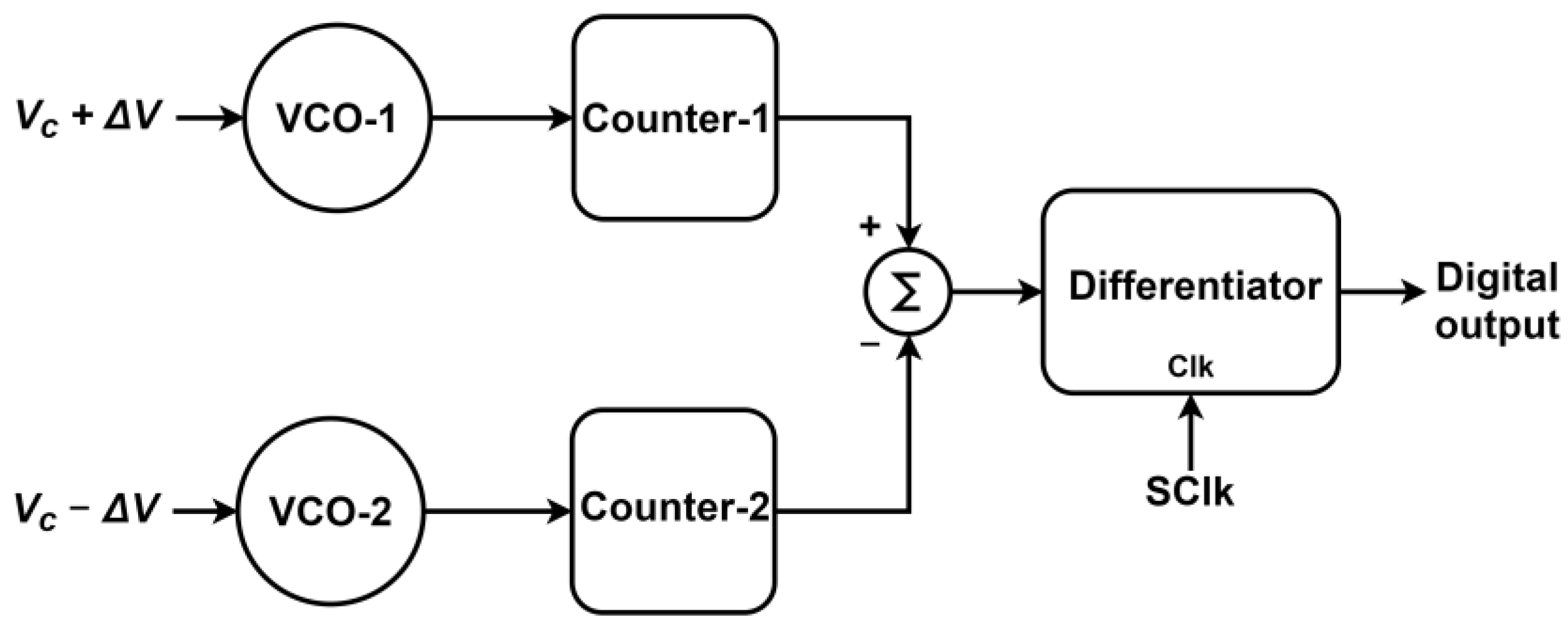
Figure 2.
Generation of an adaptive clock.
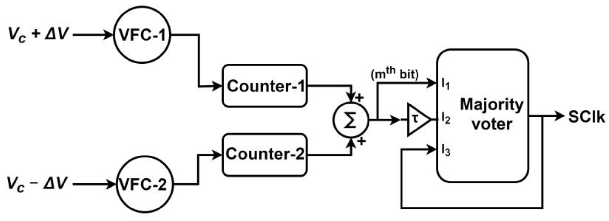
Figure 3.
Swapping of the VFC inputs and outputs.
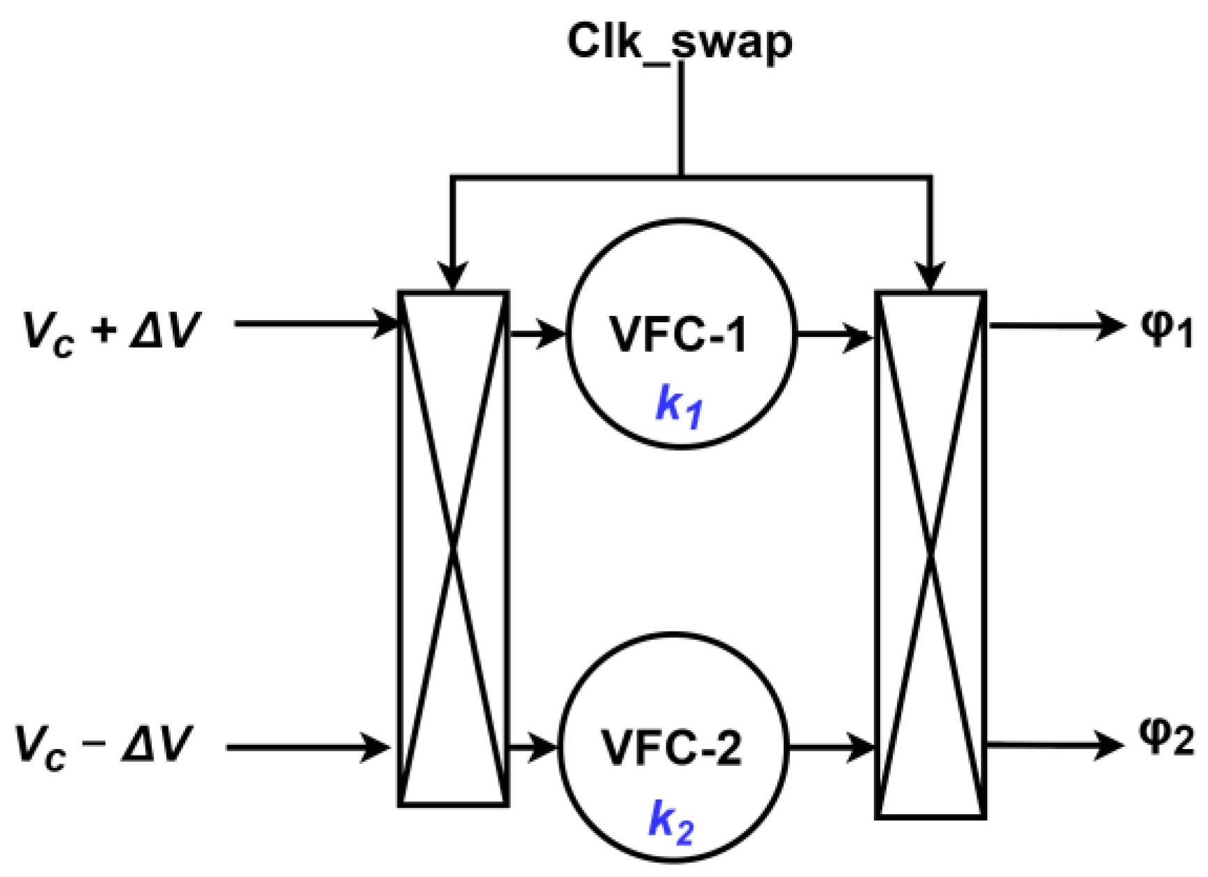
Figure 4.
Block of Architecture-1 interfaced with a full Wheatstone bridge resistive sensor.
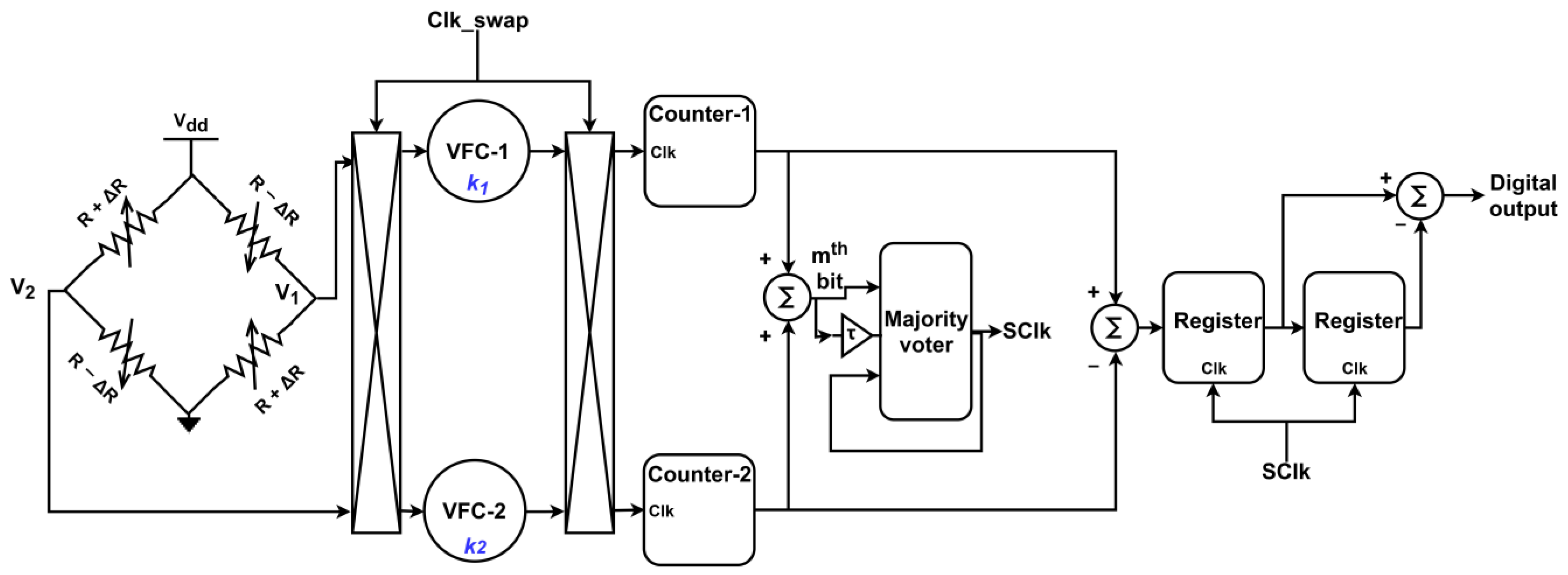
Figure 5.
Block diagram of Architecture-2.
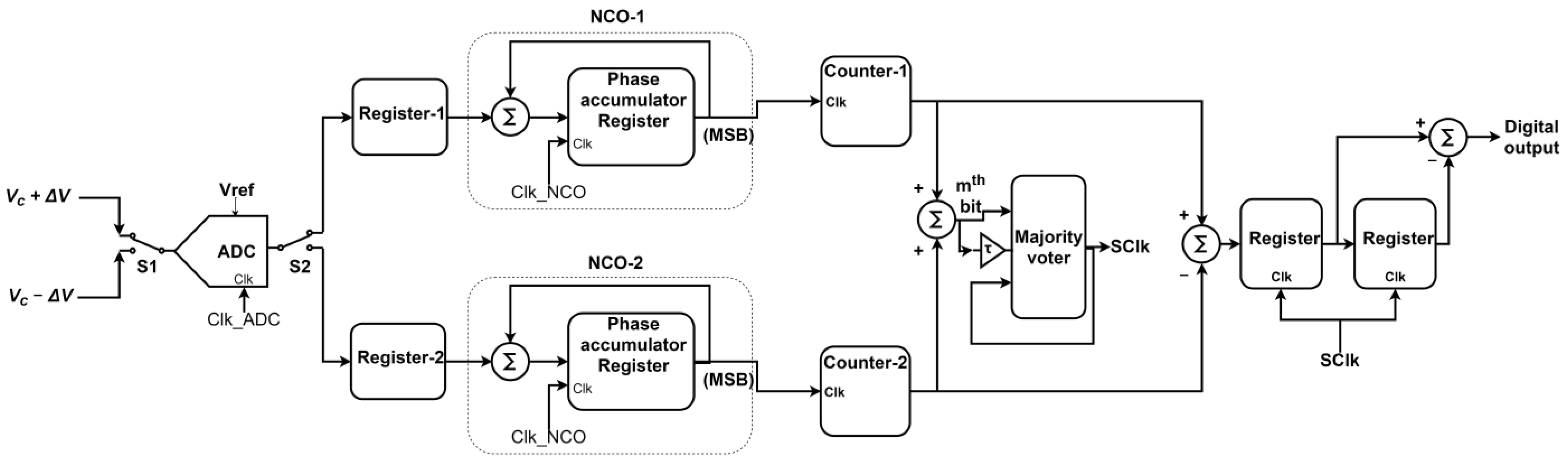
Figure 6.
Implementation of the emulated and swapped VFCs.

Figure 7.
The measured gain errors of Architecture-1 and the conventional architecture with constant frequency clock for various common mode gain drifts.
Figure 7.
The measured gain errors of Architecture-1 and the conventional architecture with constant frequency clock for various common mode gain drifts.
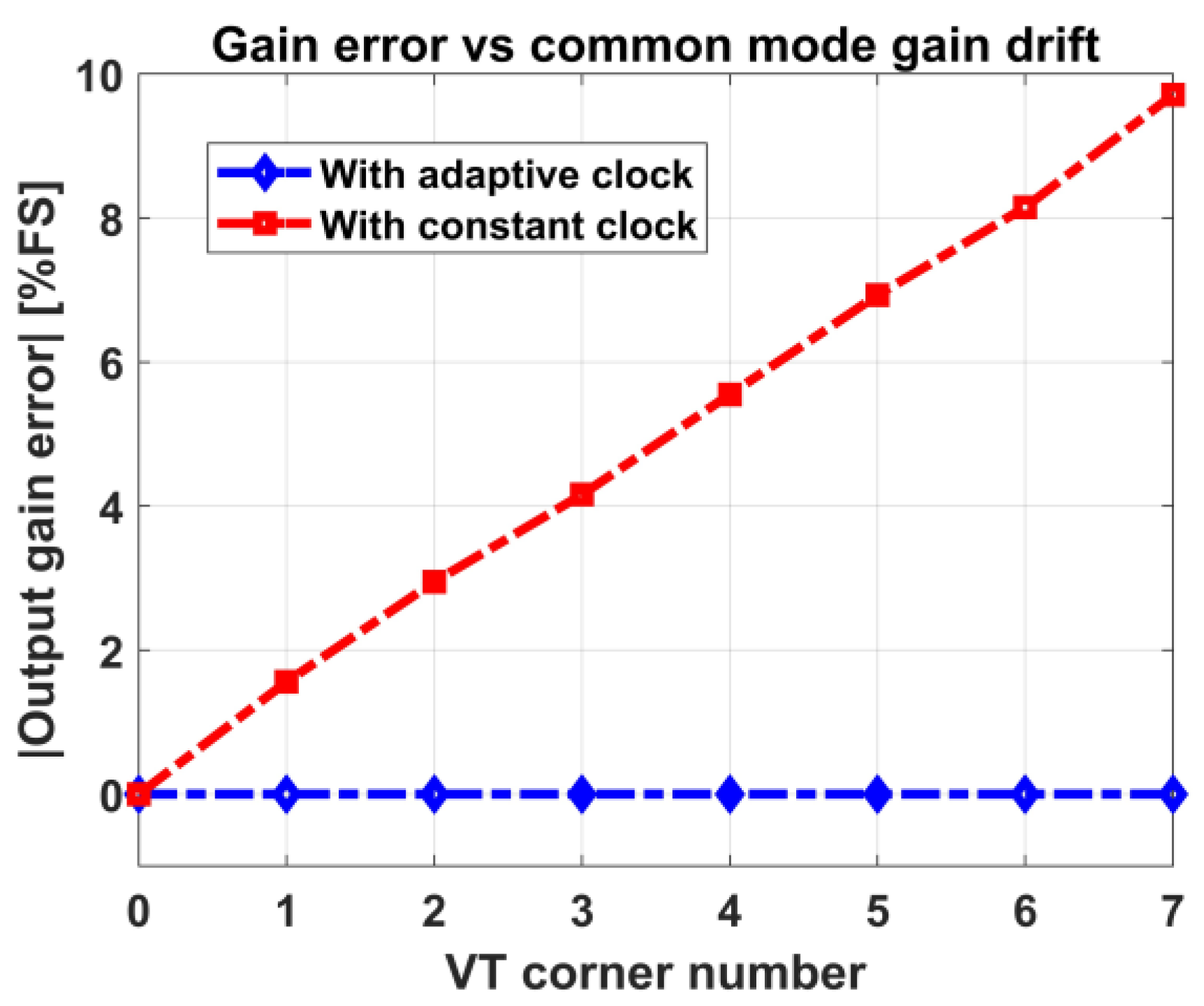
Figure 8.
PSD plot of the output of Architecture-1 for two extreme VT corner numbers with an adaptive clock and parameters listed in Table 2.
Figure 8.
PSD plot of the output of Architecture-1 for two extreme VT corner numbers with an adaptive clock and parameters listed in Table 2.
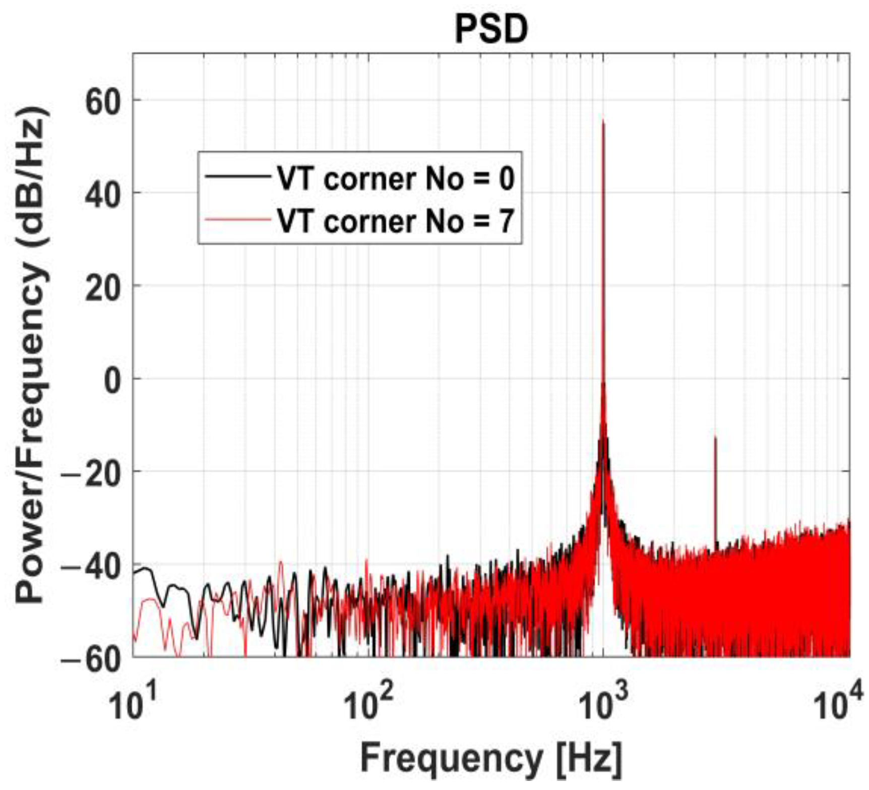
Figure 9.
Two possible sources of the swapping clock.

Figure 10.
PSD for two cases of swapping clock sources under a 6.25% mismatch between the two VFCs.
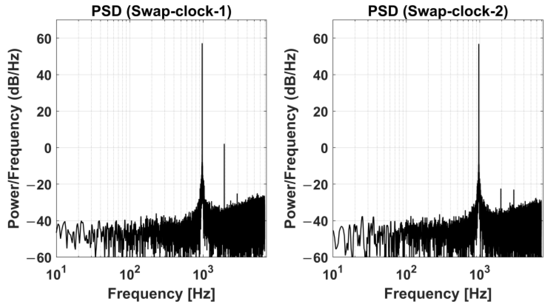
Figure 11.
System performance for various VFC gain mismatch values: (a) Offset error; (b) Gain error.
Figure 11.
System performance for various VFC gain mismatch values: (a) Offset error; (b) Gain error.
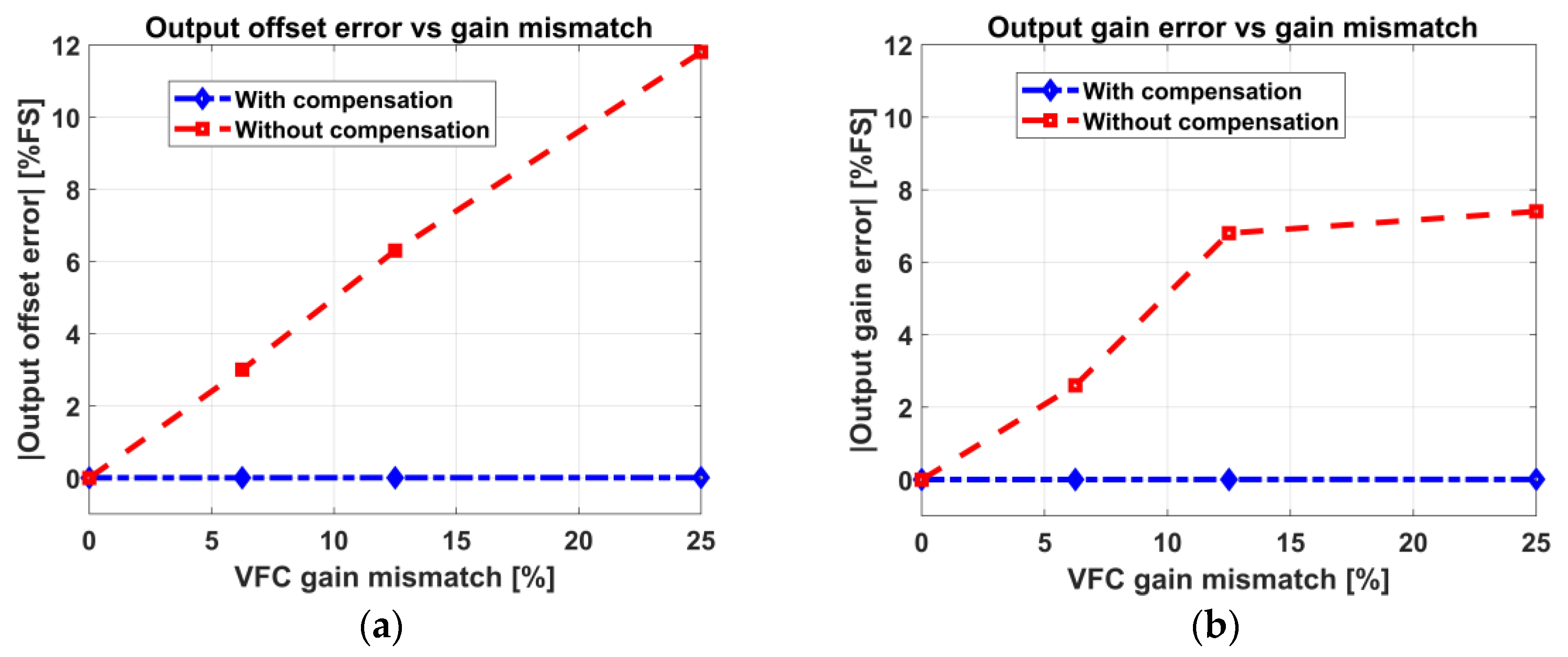
Figure 12.
PSD of Architecture-1 for three mismatch values.
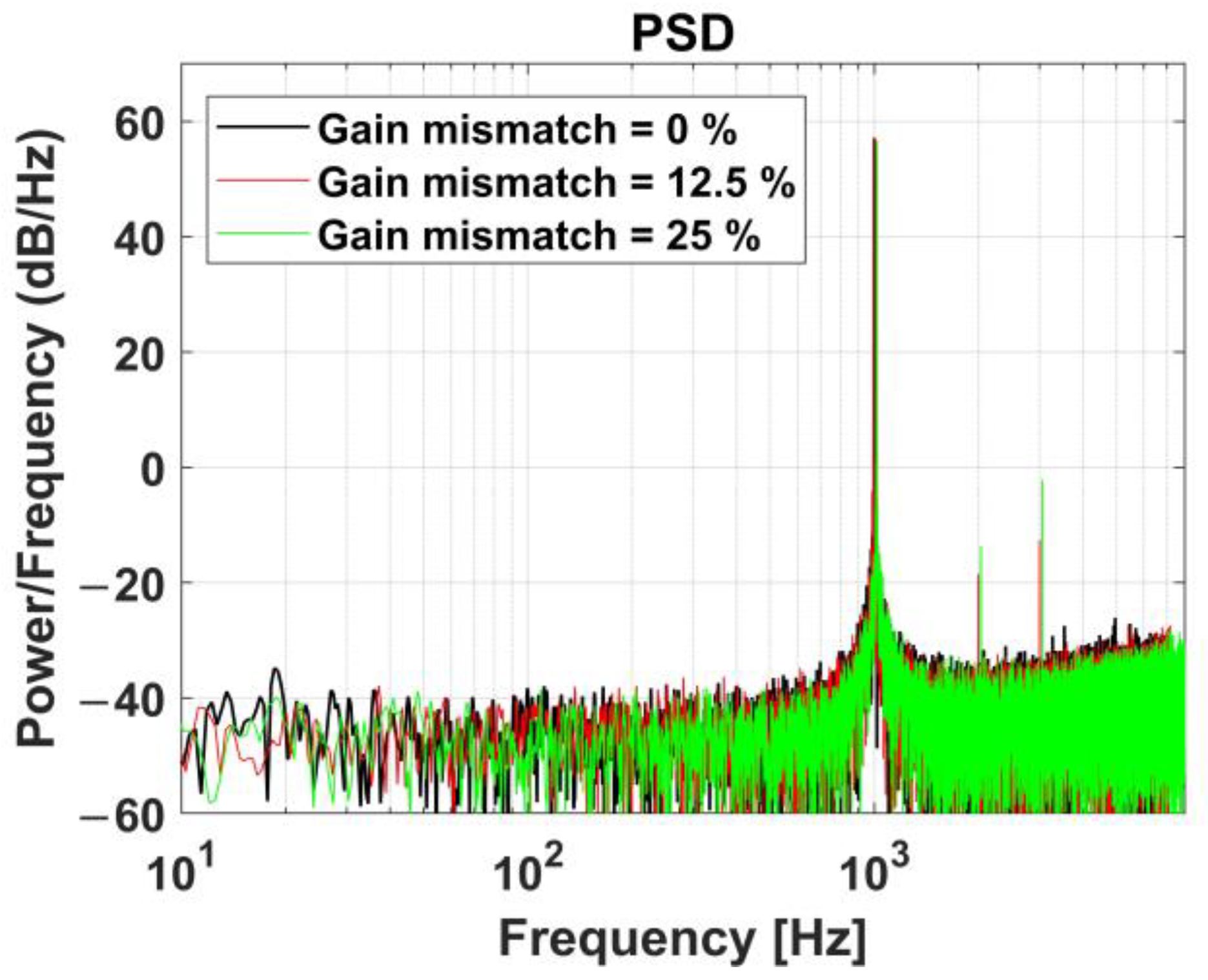
Figure 13.
Dynamic performance of Architecture-1 for variable mismatches: (a) SNDR; (b) SFDR.

Figure 14.
PSD plot of the output of Architecture-2.

Figure 15.
Output gain error vs. emulated supply drift for Architecture-2.


Table 1.
Variation of the internal voltage and temperature with the number of ring oscillators.
| Voltage, Temperature (VT) Corner Number | N° of Heating Ring Oscillators | Chip Temperature (°C) | Internal Voltage (V) |
|---|---|---|---|
| 0 | 0 | 47.5 | 0.991 |
| 1 | 250 | 51 | 0.987 |
| 2 | 500 | 54.5 | 0.983 |
| 3 | 750 | 57.5 | 0.979 |
| 4 | 1000 | 61 | 0.974 |
| 5 | 1250 | 64.5 | 0.971 |
| 6 | 1500 | 67 | 0.967 |
| 7 | 1750 | 70.5 | 0.963 |
Table 2.
List of parameters used in the implementation of Architecture-1.
| Parameters | Values |
|---|---|
| m | 11 |
| fin (KHz) | 1 |
| Bandwidth (KHz) | 10 |
| VFC sensitivity (MHz/Vp-p) | 25 |
| VFC center frequency, fc (MHz) | 25 |
Table 3.
List of parameters used in the implementation of Architecture-2.
| Parameters | Values |
|---|---|
| m | 11 |
| Apk (mV) | 250 |
| Vc (mV) | 500 |
| fin (kHz) | 1 |
| Bandwidth (kHz) | 10 |
| (bits) | 14 |
| ADC resolution (bits) | 12 |
| fc (MHz) | 25 |
| (MHz) | 200 |
| (MHz) | 200 |
Table 4.
Comparison with prior works.
| [12] | [21] | [18] | [25] | [26] | [27] | This Work (Architecture-2) | |
|---|---|---|---|---|---|---|---|
| Topology | Closed-loop (PLL-based) | Open-loop differential | Open-loop single-ended | Open-loop differential | Open-loop differential | Open-loop single-ended | Open-loop differential |
| Technology | 130 nm CMOS | 40 nm CMOS | 65 nm CMOS | 180 nm CMOS | 180 nm CMOS | 180 nm CMOS | ZYBO implementation |
| Application | Resistive sensor | General purpose | Resistive sensor | Resistive sensor | Resistive sensor | Resistive sensor | General purpose |
| Technique | Force-balanced Wheatstone bridge | Time ratio | Digital output ratio | Voltage ratio | Resistance ratio | Time domain comparison with resistive DAC | Frequency ratio |
| Sampling frequency (kHz) | 20 | 2100 | 12.5 | 8 | 1 | 5.5 | 25.5 |
| Bandwidth (kHz) | 10 | 700 | 1 | 0.06 | - | 2.3 | 10 |
| ENOB | 8.9 | 7.6 | 7.3 | 13 | 7.9 | 7.6 | 8.6 |
| Supply sensitivity (%/V) | 2.33 | 1.42 | 3.6 | 0.23 | 6.8 | 0.65 | 0.2 |
Disclaimer/Publisher’s Note: The statements, opinions and data contained in all publications are solely those of the individual author(s) and contributor(s) and not of MDPI and/or the editor(s). MDPI and/or the editor(s) disclaim responsibility for any injury to people or property resulting from any ideas, methods, instructions or products referred to in the content. |
© 2023 by the authors. Licensee MDPI, Basel, Switzerland. This article is an open access article distributed under the terms and conditions of the Creative Commons Attribution (CC BY) license (https://creativecommons.org/licenses/by/4.0/).
Share and Cite
MDPI and ACS Style
Zenebe, M.B.; Alemu, G.; De Smedt, V.; Leroux, P. Drift Resilient Frequency-Based Sensor Interface Architectures with Adaptive Clock Frequency. Electronics 2023, 12, 2775. https://doi.org/10.3390/electronics12132775
AMA Style
Zenebe MB, Alemu G, De Smedt V, Leroux P. Drift Resilient Frequency-Based Sensor Interface Architectures with Adaptive Clock Frequency. Electronics. 2023; 12(13):2775. https://doi.org/10.3390/electronics12132775
Chicago/Turabian StyleZenebe, Mikias Belhu, Getachew Alemu, Valentijn De Smedt, and Paul Leroux. 2023. "Drift Resilient Frequency-Based Sensor Interface Architectures with Adaptive Clock Frequency" Electronics 12, no. 13: 2775. https://doi.org/10.3390/electronics12132775
Note that from the first issue of 2016, this journal uses article numbers instead of page numbers. See further details here.