
Design of UWB Filtering Impedance Transformers and Power Dividers Using Stepped-Impedance Resonators

1
College of Electronic and Information Engineering, Nanjing University of Aeronautics and Astronautics, Nanjing 210016, China
2
The 55th Research Institute, China Electronics Technology Group Corp., Nanjing 210016, China
3
Department of Aeronautics & Astronautics, Institute of Space Technology, Islamabad 44000, Pakistan
*
Author to whom correspondence should be addressed.
Electronics 2023, 12(13), 2800; https://doi.org/10.3390/electronics12132800
Submission received: 8 May 2023
/
Revised: 5 June 2023
/
Accepted: 12 June 2023
/
Published: 25 June 2023
(This article belongs to the Special Issue Microwave Devices: Analysis, Design, and Application)
Abstract
:This study presents a novel design of ultra-wideband (UWB) impedance transformers and power dividers with filtering capabilities. Based on the UWB impedance matching network, the UWB filtering impedance transformers are designed, and the UWB filtering power dividers are achieved by impedance transforming one port of one or more impedance transformers. The transformers consist of a multi-mode stepped-impedance resonator (SIR) and defected ground structures (DGSs). The SIR is tightly coupled to two ports of different impedance levels via the unsymmetrical two-sided coupled lines and DGSs. In addition, two transformers that convert impedance from 50 Ω to 100 Ω are connected to form a UWB power divider with filtering function. The 25 Ω port of an impedance transformer with a 50 Ω to 25 Ω conversion is impedance matched to two 50 Ω ports connected in parallel, resulting in another power divider with filtering function. Thus, two prototype UWB impedance transformers from 50 Ω to 100 Ω and from 50 Ω to 25 Ω are designed and their corresponding power dividers are also designed and fabricated. The simulated and measured results are consistent, demonstrating good features, such as return loss greater than 10 dB and insertion loss less than 4.5 dB in the passband, UWB filtering capacity with out-of-band rejection greater than 20 dB, and compact size smaller than 1.2λ × 2.1λ (λ is the wavelength of the central frequency).
1. Introduction
Owing to its potential applications in telecommunications, radars, and other systems, the research on ultra-wideband (UWB) technologies has attracted a lot of attention. UWB impedance transformers, filters, and power dividers are the key components to construct UWB circuits and systems, such as UWB antenna arrays [1,2,3,4] and UWB power amplifiers [5]. In the past, UWB impedance transformers and power dividers were realized with multiple quarter-wavelength sections [6] or with Klopfenstein impedance tapers [3] but entailed the shortcoming of large dimensions. Various methodologies have been reported to minimize these dimensions in the past two decades. A T-junction formed by slot and microstrip lines, together with a wideband transition, is used to design UWB power dividers [7]. Another divider with two substrate layers was designed by providing coupling between top and bottom microstrip lines via the aperture of the common ground layer [8]. However, the complex multi-layer PCB manufacturing is required. An UWB power divider was realized by introducing one butterfly radial stub on each branch to obtain UWB performance [9]. A two-section UWB power divider was also proposed and filtering was introduced by adding open stubs for improving high-frequency suppression and using interdigital couplings for improving low-frequency suppression [10]. F. Wei presented an UWB power divider with a rejected band by using shunt-stub filtering sections coupled with folded stepped-impedance resonators (SIRs), but the SIRs were used to generate narrow notch-band and were not applicable to generate UWB passband [11].
Multiple-mode SIRs have been applied to realize bandpass filters, especially UWB ones [12,13,14,15,16,17,18]. The UWB bandpass filters are realized introducing tight couplings between the SIR and the two-sided ports, and all the resonating modes are employed to form an UWB passband. Commonly, the tight couplings may be realized with interdigital couplings or using aperture-based interdigital couplings, and the two-sided couplings are always symmetrical.
Unlike the symmetric structure for realizing UWB filters in [14,15,16,17,18], unsymmetrical tight couplings containing DGSs at two sides of an SIR are used in this paper to realize impedance transformers. In addition, filtering power dividers based on UWB impedance transformers are proposed and designed. In [19], a balanced-to-balanced in-phase filtering power divider based on microstrip/slotline transition structures and slotline T-junction was proposed, and the sharp filtering performance was realized by introducing the microstrip stub-loaded resonators. Although some filtering power dividers have been mentioned, they are rarely mentioned in the use of the UWB characteristics of SIR to UWB impedance matching and in the use of this impedance matching network to design a power divider. The UWB power divider with DC-blocking based on impedance matching network is necessary to research its flexible design and wide application scenarios.
2. Structure, Design Method, and Results of UWB Filtering Impedance Transformer
2.1. Design Concept and Theory
A multi-mode resonator, such as an SIR, has several resonating modes distributed within a UWB pass band. Figure 1 shows the circuit of a UWB bandpass filter containing an SIR, which is tightly coupled to two-sided ports with interdigital-coupled lines. The equivalent circuit is also given in Figure 1, and every interdigital coupling line can be equivalent to a sub-network containing the center J inverter and two-sided high-impedance lines. The center part of the whole network as an equivalent SIR has several resonating modes that can be equally spaced within a UWB passband by optimizing the lengths and characteristic impedances of the sections. Considering there is no coupling between the resonating modes of an SIR, every mode is independently coupled to the two-sided ports, and we can give the conceptual topology of a UWB bandpass filter, as shown in Figure 2a. Since the UWB bandpass filter is in a symmetric structure, we may find that the two-sided J inverters are the same.
For converting the UWB filter to a UWB filtering impedance transformer (from Z0 to nZ0), the impedance at port 1 remains unchanged while that at port 2 is updated with nZ0. This condition can be satisfied if every input impedance Zini of Figure 2a equals that of Figure 2b because every coupling path of Figure 2 works at a separate frequency band and is unaffected by other paths. We have
which can be rearranged as
2.1.1. Theory of Parallel-Coupled Lines
For the single-section parallel-coupled lines in Figure 3a, the scattering matrix can be expressed as follows due to the structural symmetry [6]:
When even-mode and odd-mode voltages are applied to ports 1 and, 3 respectively, the four-port network in Figure 3a can be simplified to the two-port networks shown in Figure 3b,c. The even- and odd-mode scattering matrices of two-port networks can be expressed as
and the normalized transmission matrices can be expressed as
where θ, Z0o, and Z0e are the equivalent electrical length, the characteristic impedances of odd-mode and even-mode, respectively.
From the conversion equation of the scattering matrix of two-port network, S, to the transmission matrix of two-port network, A, in [6]
and we have
From the definition of the scattering matrix in [6], we have the relationship between the input and output of the single-section parallel-coupled lines,
For the parallel-coupled lines with open ends on both sides of Figure 3a, b2 = a2 and b3 = a3 can be obtained. From Equation (8), we get
and thus, for the dual ports’ parallel-coupled lines in Figure 4, we have
The scattering matrix can be obtained as follow:
According to the Equation (6), convert the scattering matrix of the parallel-coupled lines in Figure 4 to the transmission matrix, and we can get
For a J inverter, its ABCD matrix can be expressed as
As shown in Figure 4, the dual ports’ parallel-coupled lines are equivalent to the J inverter. Combining Equations (9) and (10), we can get the relationship between the ratio of the even-mode characteristic impedance, Z0e, to the odd-mode characteristic impedance, Z0o, of the parallel-coupled line and J in Figure 5. It can be seen that |J| increases with the increase in the ratio, which means that greater J requires stronger coupling.
Equation (2) implies that the couplings at two sides are unsymmetrical, and the output coupling is tighter than the input coupling when n > 1. Notably, the input impedance from port 2 is nZ0. It is theoretically feasible to design an UWB impedance transformer with arbitrary impedance ratio by changing the coupling strength ratio of the input and output coupling structures. In practice, the coupling can be enhanced by widening the width of DGS and increasing the number of interdigital figures.
2.1.2. Theory of Defected Ground Structure
As shown in Figure 6a, for the microstrip-coupled lines, three types of capacitance are distributed between each microstrip line and the bottom metal layer of the substrate in the even-mode model, namely, the outer-edge distribution capacitance Cf, the middle distribution capacitance Cp, and the inner-edge distribution capacitance Cf’, while the outer-edge distribution capacitance Cf, the middle distribution capacitance Cp, the electrical wall capacitance in the air Cga, and the electrical wall capacitance in the substrate between two microstrip lines Cgd are distributed in the odd-mode model. The characteristic impedances of microstrip-coupled lines can be expressed as
where vpe1 and vpo1 are phase velocities of even/odd modes. Compared to microstrip-coupled lines, DGS-loaded coupled lines lack the middle distribution capacitance Cp and the inner-edge distribution capacitance Cf’, and the outer-edge distribution capacitance varies with the width of the DGS, as shown in Figure 6b, whose characteristic impedance can be expressed as
Considering that vpe1, vpo1, vpe2, and vpo2 have close value, we have
which means placing DGS under microstrip lines could enhance the coupling and increase |J| of J inverter [20].
2.2. UWB Filtering Transformer from 50 Ω to 100 Ω
Figure 7 shows the proposed filtering UWB impedance transformer from 50 Ω to 100 Ω where the SIR and unsymmetrical DGS-based coupling structures are applied. By using a wider DGS and by increasing the number and length of interdigital coupled fingers at the 100 Ω port (port 2), we achieve good matching at two ports, and a return loss better than 13 dB across the UWB passband can be shown in Figure 8.
Figure 8 also shows the S-parameters of transformers under different conditions. Compared with the case without DGSs [17], the return loss improves when DGSs are added at the two sides with larger S (S = 0.1 mm) as a 1st step and more interdigital fingers in the 2nd step. Table 1 presents the dimensions of this impedance transformer after optimization. Figure 9 shows the E field and H field of the impedance transformer from 50 Ω to 100 Ω at different frequencies.
The proposed filtering UWB impedance transformer from 50 Ω to 100 Ω is implemented on a RT/Duroid 6010 substrate with thickness of h = 1.27 mm and dielectric constant of εr = 10.8. In measurement, the 100 Ω port of impedance transformer is connected to a 100 Ω resistor, of which the remaining end is grounded with metal via holes, while the 50 Ω port is soldered with an SMA connector.
Figure 10 shows the simulated and measured results of the designed UWB impedance transformer. The graph reveals that the measured return loss of the proposed impedance transformer is better than 10 dB within the UWB frequency range of 3.6–10.3 GHz, which proves the validity of the presented solutions. The frequency shift is mainly caused by tolerances in fabrication and measurement.
Figure 11 shows the photographs of the fabricated UWB impedance transformer. The overall structural dimension without SMA connector is approximately 7.9 × 25 mm, and the length is approximately 1.8 wavelengths (1.8λ) at the central frequency of 6.85 GHz.
2.3. UWB Filtering Transformer from 50 Ω to 25 Ω
Figure 12 shows another filtering UWB impedance transformer from 50 Ω to 25 Ω. Similar with the 50 Ω to 100 Ω transformer, DGSs are used to increase the couplings for impedance transformation.
Equation (2) shows that the 50 Ω end of the impedance transformer needs stronger coupling than the 25 Ω end; hence, the DGS is adopted under the parallel-coupled line of the 50 Ω end. It can be seen from Figure 13b that when the frequency is less than 6 GHz, the insertion loss curve moves up with the increase in W2, while when the frequency is greater than 6 GHz, the S21 curve moves up first and then down with the increase in W2. This shows that only changing the coupling strength of the 50 Ω port cannot meet the coupling relationship in Equation (2); hence, the DGS is used near the 25 Ω port. Figure 14 shows the simulated S parameters as W4 increases when W2 = 1.1 mm. The dimensions of this impedance transformer after optimization are listed in Table 2. The E field and H field of the impedance transformer from 50 Ω to 25 Ω at different frequencies are given in Figure 15.
The proposed filtering UWB impedance transformer (from 50 Ω to 25 Ω) is also implemented on a RT/Duroid 6010 substrate but with a smaller thickness of h = 0.254 mm. In practice, the non-50 Ω terminal of impedance transformer is often connected to the load network for use, and it is difficult to find the SMA connector with non-50 Ω impedance. Therefore, for convenience of measurement, the 25 Ω port of impedance transformer is loaded with a 24 Ω surface-mounted resistor.
Figure 16 shows the simulated and measured S11. The S11 of the 50–25 Ω impedance transformer is better than −10 dB from 4 GHz to 10.6 GHz. Although not measured, the transmission coefficient S21 from port 1 to 2 can be computed roughly as
Figure 17 shows the photograph of the fabricated UWB impedance transformer with an overall dimension of approximately 5.6 × 24.8 mm.
3. Structures and Results of UWB Filtering Power Dividers
3.1. UWB Filtering Power Divider Based on Impedance Transformers from 50 Ω to 100 Ω
Figure 18 shows that an UWB filtering power divider can be constructed by simply connecting the 100 Ω ports of two UWB 50 Ω to 100 Ω impedance transformers. Given that the input impedances Zin1 and Zin2 are 100 Ω, we can obtain 50 Ω input impedance at port 1 of the power divider. The simulation results of the above power divider are shown in Figure 19. It can be seen from the curve that the power divider has good out-of-band harmonic rejection.
Figure 20 shows the comparison of simulated and measured results. Due to the measuring range of the test instrument, only the S-parameters before 13 GHz are shown here. Across the frequency band from 3.1 GHz to 9.5 GHz, the simulated insertion loss |S21|(|S31|) is approximately 3.4 dB and the return loss |S11| is better than 10 dB. Compared with the simulation results, the measured passband is shifted upward, covering a frequency range from 4 GHz to 10 GHz, mainly due to manufacturing tolerance. The measured return loss is better than 10 dB throughout the pass band. The insertion loss is approximately 3.6 dB in the range from 4 GHz to 8.4 GHz, 4.1 dB in the range from 8.4 GHz to 9.4 GHz, and 4.5 dB in the range from 9.4 GHz to 10 GHz. The rejection is larger than 30 dB from 12.5 GHz above. Within the UWB passband from 3.1 GHz to 9.5 GHz, the simulated and measured group delay between port 1 and port 2 are both less than 0.5 ns, and the in-band fluctuation of measured group delay is less than 0.3 ns as shown in Figure 21. Due to the symmetry of the structure, the group delay curve between ports 1 and 3 overlap with those of ports 1 and 2 and is not shown here.
As can be seen from Figure 20, there is a singular point at around 12.8 GHz. It is caused by the loading effect of the strong coupling structure at both ends of two parallel transformers. It is mentioned in [13] that multi-mode stepped-impedance resonator has multiple resonant modes. When several resonant frequencies get close, a passband can be formed. The strong coupling structures at both ends of the two parallel transformers in Figure 18 change the resonance modes distribution of SIR; hence, singular point is formed at around 12.8 GHz of the stopband. The singular point can be eliminated by optimizing the impedance ratio of each transmission line of SIR.
Figure 22 shows the fabricated UWB filtering power divider with dimensions of 17 × 28 mm, which is 1.2λ × 2.1λ at 6.85 GHz.
3.2. UWB Filtering Power Divider Based on Impedance Transformers from 50 Ω to 25 Ω
Figure 23 shows another UWB filtering power divider that is formed by dividing the 25 Ω port of a UWB impedance transformer (from 50 Ω to 25 Ω) into two 50 Ω ports. Within the UWB band from 4 GHz to 10.6 GHz, the simulated insertion loses are approximately 3.4 dB as shown in Figure 24.
Figure 25 shows that the return loss is better than 11 dB. The proposed filtering UWB power divider is implemented on the RT/Duroid 6010 substrate with a thickness of h = 0.254 mm and dielectric constant of εr = 10.8. Figure 25 also shows the comparison between the simulated and measured results of designed UWB filtering power divider. The measured results reveal that the insertion loss varies between 3.5 dB to 4.4 dB. As seen from the graph, the measured S11 of the proposed impedance transformer is well below −11 dB within the UWB band of 4 GHz to 11 GHz. Insertion loss is well over 20 dB after 12 GHz, which proves the validity of the presented solutions for UWB filtering.
In addition, the UWB power divider composed of a single transformer (from 50 Ω to 25 Ω) has no singular point in the stopband because the strong coupling structures at both ends of the transformer are only composed of DGSs. The loading effect of strong coupling structures has little impact on the resonant frequencies’ distribution of SIR.
Figure 26 shows the simulated and measured group delay between port 1 and port 2 of UWB filtering power divider composed of a single transformer (from 50 Ω to 25 Ω). Within the UWB passband from 4 GHz to 10.6 GHz, the simulated and measured group delay are both less than 0.51 ns with the maximum variation of about 0.18 ns, thus, implying the good linearity of this proposed UWB filtering power divider.
Figure 27 shows the photographs of UWB filtering power divider with the dimensions of approximately 6.6 × 23.6 mm (0.5λ × 1.74λ at the center frequency of 6.85 GHz). Given that only one transformer is used, the width is sharply reduced.
3.3. Discussions
This paper mainly presents the design methods of UWB filtering impedance transformer based on SIR and UWB filtering power divider using this transformer. The method of improving frequency selectivity of filter based on SIR has been mentioned in some articles and will not be discussed in depth in this paper. In [18], two capacitive-ended interdigital coupled lines are used to generate transmission zeros for great frequency selectivity. Furthermore, a method where tapped-line input/output structures are exploited to create extra transmission zeros in the stopband was mentioned in [21].
Table 3 shows the performance comparison between the proposed UWB power dividers and those of published works [8,9,10,11]. Compared with previous designs, the present dividers feature good UWB filtering performance. In addition, although the return loses and insertion loses are similar for all designs, the proposed UWB power dividers are much smaller than previous ones.
The proposed UWB power dividers are suitable for the feed networks of antenna array, and their isolations are similar to that of traditional Y-type power divider. The UWB power divider containing one 50 Ω to 25 Ω impedance transformers is much smaller and simpler than that containing two 50 Ω to 100 Ω. However, the latter provides higher isolation between ports 2 and 3 if an isolating resistor is used. Due to different levels of characteristic impedance, the former is suitable for applications using substrates with higher dielectric constant or smaller thickness.
4. Conclusions
The novel design of UWB filtering impedance transformers and power divider is presented and implemented in this study. The impedance transformers are proposed by introducing unsymmetrical tight couplings at the two ends of an SIR, and the coupling strength on both sides of the SIR can be adjusted by unsymmetrical widths of DGS and different numbers of interdigital figures to optimize the transmission performances. The impedance transformers from 100 Ω to 50 Ω and from 25 Ω to 50 Ω are designed, fabricated, and measured, and good UWB impedance transforming and filtering performances are achieved in compact dimensions. The non-50 Ω ports of the above two impedance transformers are matched by impedance to obtain two power dividers, and good UWB filtering is well inherited. The measured results of the UWB filtering power dividers demonstrate good features, such as low insertion loses and great VSWR, considerable out-of-band rejection, and compact size, proving the potential of being used in a variety of RF front-end systems, especially the feeding networks of UWB antenna arrays.
Author Contributions
Conceptualization, Y.L.; methodology, Z.C. and Y.L.; software, Z.C. and C.L.; validation, Z.C.; formal analysis, Y.L.; investigation, Z.C.; resources, Y.L.; data curation, Z.C. and C.L.; writing—original draft preparation, Z.C.; writing—review and editing, Y.L. and I.M.; visualization, Z.C. and C.L.; supervision, Y.L. and I.M.; funding acquisition, Y.L. All authors have read and agreed to the published version of the manuscript.
Funding
This work was supported by the National Natural Science Foundation of China (Grant No. 62071228).
Data Availability Statement
The data can be shared upon request.
Conflicts of Interest
The authors declare no conflict of interest.
References
- Cao, Z.; Chen, Y.; Meng, H. A W-Band Two-Dimensional Monopulse Sparse Array Antenna. IEEE Trans. Antennas Propag. 2022, 70, 9260–9269. [Google Scholar] [CrossRef]
- Lakrit, S.; Medkour, H.; Das, S.; Madhav, B.T.P.; Ali, W.A.E.; Dwivedi, R.P. Design and analysis of integrated Wilkinson power divider-fed conformal high-gain UWB array antenna with band rejection characteristics for WLAN applications. J. Circuits Syst. Comput. 2021, 30, 2150133. [Google Scholar] [CrossRef]
- Zhang, T.; Chen, L.; Zaman, A.U.; Yang, J. Ultra-wideband millimeter-wave planar array antenna with an upside-down structure of printed ridge gap waveguide for stable performance and high antenna efficiency. IEEE Antennas Wirel. Propag. Lett. 2021, 20, 1721–1725. [Google Scholar] [CrossRef]
- Ghimire, J.; Choi, D.-Y. Ultra-Wide Band Double-Slot Podal and Antipodal Vivaldi Antennas Feed by Compact Out-Of-Phase Power Divider Slot for Fluid Properties Determination. Sensors 2022, 22, 4543. [Google Scholar] [CrossRef] [PubMed]
- Ali, A.; Yun, J.; Giannini, F.; Ng, H.J.; Kissinger, D.; Colantonio, P. 168–195 GHz power amplifier with output power larger than 18 dBm in BiCMOS technology. IEEE Access 2020, 8, 79299–79309. [Google Scholar] [CrossRef]
- Pozar, D.M. Microwave Engineering; John Wiley & Sons: Hoboken, NJ, USA, 2011. [Google Scholar]
- Bialkowski, M.E.; Abbosh, A.M. Design of a compact UWB out-of-phase power divider. IEEE Microw. Wirel. Compon. Lett. 2007, 17, 289–291. [Google Scholar] [CrossRef]
- Abbosh, A.; Bialkowski, M.E.; Mazierska, J. An UWB planar out-of-phase power divider employing microstrip-slot and parallel stripline-microstrip transitions. In Proceedings of the 2006 Asia-Pacific Microwave Conference, Yokohama, Japan, 12–15 December 2006; pp. 905–908. [Google Scholar]
- Zhou, B.; Wang, H.; Sheng, W. A novel UWB Wilkinson power divider. In Proceedings of the 2nd International Conference on Information Science and Engineering, Hangzhou, China, 4–6 December 2010; pp. 1763–1765. [Google Scholar]
- Liu, W.-Q.; Wei, F.; Pang, C.-H.; Shi, X.-W. Design of a compact ultra-wideband power divider. In Proceedings of the 2012 International Conference on Microwave and Millimeter Wave Technology (ICMMT), Shenzhen, China, 5–8 May 2012; pp. 1–3. [Google Scholar]
- Wei, F.; Chen, L.; Shi, X.-W.; Wu, Q.-Y.; Huang, Q.-L. Design of compact UWB power divider with one narrow notch-band. J. Electromagn. Waves Appl. 2010, 24, 2343–2352. [Google Scholar] [CrossRef]
- Makimoto, M.; Yamashita, S. Compact bandpass filters using stepped impedance resonators. Proc. IEEE 1979, 67, 16–19. [Google Scholar] [CrossRef]
- Makimoto, M.; Yamashita, S. Bandpass filters using parallel coupled stripline stepped impedance resonators. IEEE Trans. Microw. Theory Tech. 1980, 28, 1413–1417. [Google Scholar] [CrossRef]
- Zhu, L.; Bu, H.; Wu, K. Aperture compensation technique for innovative design of ultra-broadband microstrip bandpass filter. In Proceedings of the 2000 IEEE MTT-S International Microwave Symposium Digest (Cat. No. 00CH37017), Boston, MA, USA, 11–16 June 2000; pp. 315–318. [Google Scholar]
- Zhu, L.; Menzel, W.; Wu, K.; Boegelsack, F. Theoretical characterization and experimental verification of a novel compact broadband microstrip bandpass filter. In Proceedings of the 2001 Asia-Pacific Microwave Conference (Cat. No. 01TH8577), Taipei, Taiwan, 3–6 December 2001; pp. 625–628. [Google Scholar]
- Menzel, W.; Zhu, L.; Wu, K.; Bogelsack, F. On the design of novel compact broad-band planar filters. IEEE Trans. Microw. Theory Tech. 2003, 51, 364–370. [Google Scholar] [CrossRef]
- Zhu, L.; Sun, S.; Menzel, W. Ultra-wideband (UWB) bandpass filters using multiple-mode resonator. IEEE Microw. Wirel. Compon. Lett. 2005, 15, 796–798. [Google Scholar]
- Sun, S.; Zhu, L. Capacitive-ended interdigital coupled lines for UWB bandpass filters with improved out-of-band performances. IEEE Microw. Wirel. Compon. Lett. 2006, 16, 440–442. [Google Scholar] [CrossRef]
- Wei, F.; Yang, Z.-J.; Qin, P.-Y.; Guo, Y.J.; Li, B.; Shi, X.-W. A balanced-to-balanced in-phase filtering power divider with high selectivity and isolation. IEEE Trans. Microw. Theory Tech. 2018, 67, 683–694. [Google Scholar] [CrossRef]
- Liu, Y.; Liu, L.; Liang, C.; Majid, I. Compact planar tunable filter with constant absolute bandwidth and wide-frequency tuning range using DGS coupling structure. IEEE Access 2021, 9, 157259–157266. [Google Scholar] [CrossRef]
- Kuo, J.-T.; Shih, E. Microstrip stepped impedance resonator bandpass filter with an extended optimal rejection bandwidth. IEEE Trans. Microw. Theory Tech. 2003, 51, 1554–1559. [Google Scholar]
Figure 1.
Equivalent circuit network of UWB filter using SIR.

Figure 2.
Topology transformation from UWB filter to UWB impedance transformer: (a) Topology of UWB filter using multi-mode resonator; (b) Topology of UWB impedance transformer.
Figure 2.
Topology transformation from UWB filter to UWB impedance transformer: (a) Topology of UWB filter using multi-mode resonator; (b) Topology of UWB impedance transformer.

Figure 3.
Parallel-coupled lines and their equivalent circuits under even- and odd-mode excitation: (a) Single-section parallel-coupled lines; (b) Equivalent circuit under even-mode excitation; (c) Equivalent circuit under odd-mode excitation.
Figure 3.
Parallel-coupled lines and their equivalent circuits under even- and odd-mode excitation: (a) Single-section parallel-coupled lines; (b) Equivalent circuit under even-mode excitation; (c) Equivalent circuit under odd-mode excitation.
Figure 4.
Parallel-coupled line with two open ends equivalent to J inverter.
Figure 5.
Correlation curve between Z0e/Z0o and J.
Figure 6.
Distribution capacitances between each microstrip line and the bottom metal layer of the substrate: (a) Microstrip-coupled lines; (b) DGS-loaded coupled lines.
Figure 6.
Distribution capacitances between each microstrip line and the bottom metal layer of the substrate: (a) Microstrip-coupled lines; (b) DGS-loaded coupled lines.
Figure 7.
Proposed UWB filtering impedance transformer (from 50 Ω to 100 Ω). Substrate: RT/Duroid 6010 with εr = 10.8 and thickness = 1.27 mm.
Figure 7.
Proposed UWB filtering impedance transformer (from 50 Ω to 100 Ω). Substrate: RT/Duroid 6010 with εr = 10.8 and thickness = 1.27 mm.
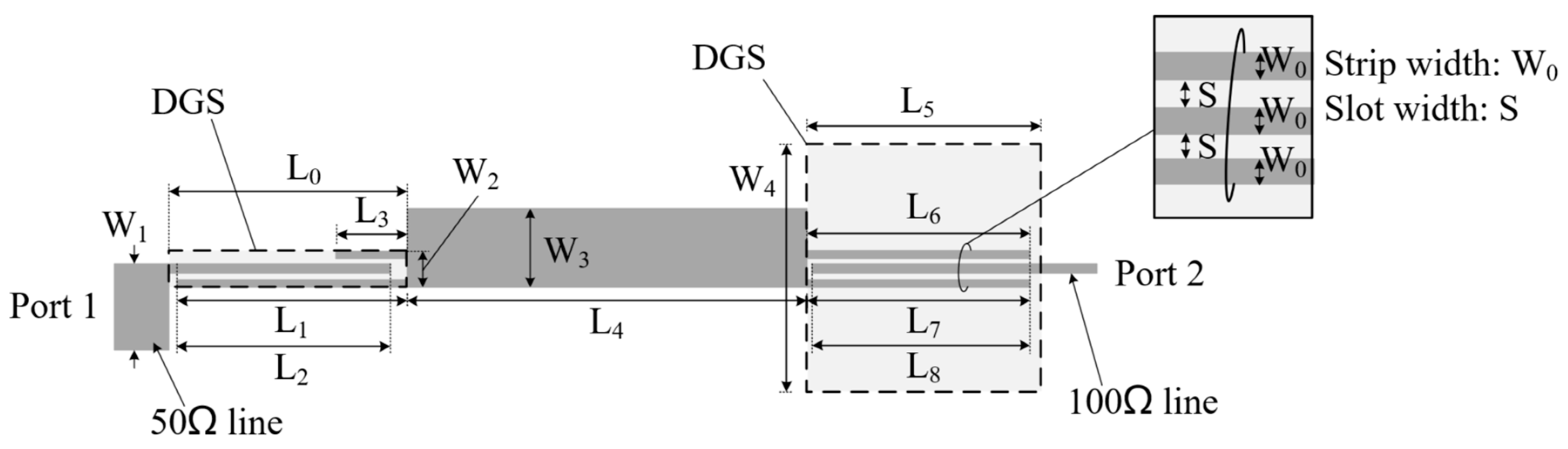
Figure 8.
Simulated S-parameters of impedance transformers (from 50 Ω to 100 Ω) with different coupling structures: (a) Only two coupled lines, slot width S = 0.1 mm, strip width W0 = 0.1 mm; (b) DGS added under coupled lines, DGS width W2 = 0.5 mm, W4 = 3.4 mm; (c) more interdigital figures added as shown in Figure 6.
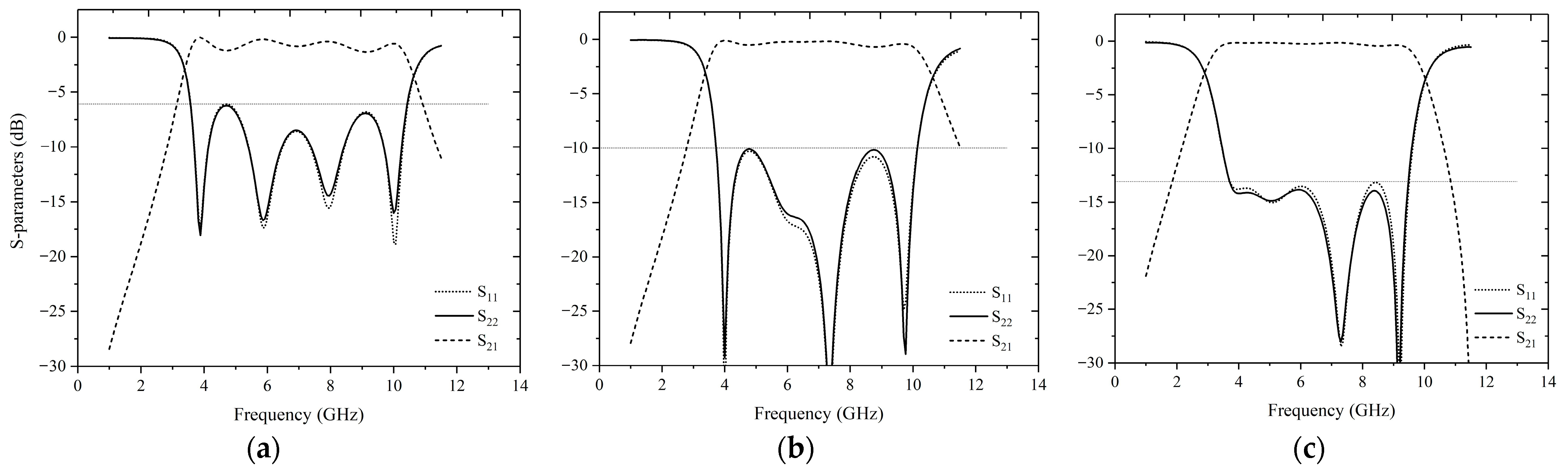
Figure 9.
E field and H field of impedance transformers (from 50 Ω to 100 Ω): (a) 2 GHz; (b) 6.85 GHz; (c) 12 GHz.
Figure 9.
E field and H field of impedance transformers (from 50 Ω to 100 Ω): (a) 2 GHz; (b) 6.85 GHz; (c) 12 GHz.

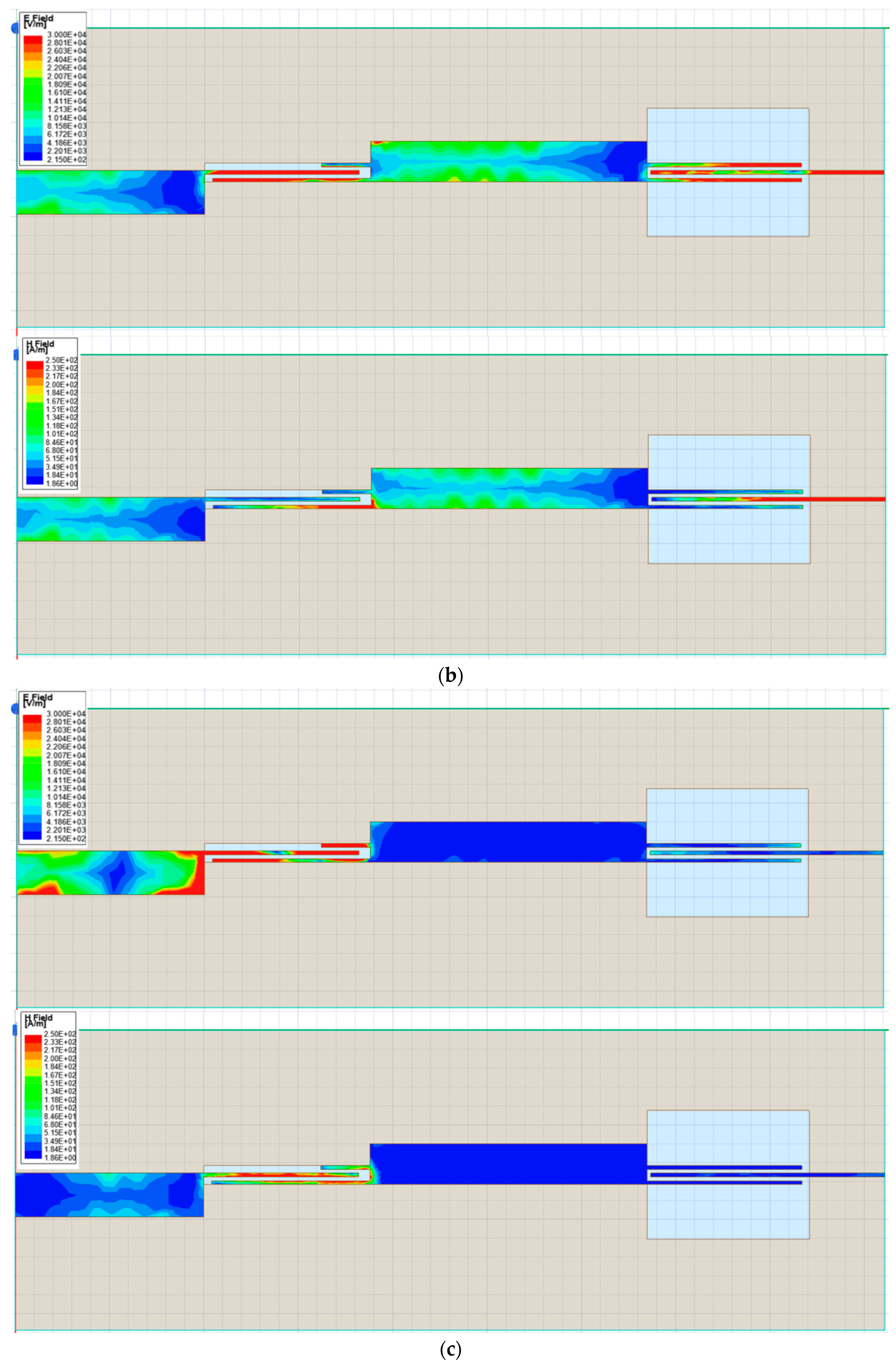
Figure 10.
Simulated and measured S-parameters of designed filtering UWB impedance transformer (from 50 Ω to 100 Ω).
Figure 10.
Simulated and measured S-parameters of designed filtering UWB impedance transformer (from 50 Ω to 100 Ω).

Figure 11.
Photographs of the fabricated filtering UWB impedance transformer (from 50 Ω to 100 Ω): (a) Top view; (b) Bottom view.
Figure 11.
Photographs of the fabricated filtering UWB impedance transformer (from 50 Ω to 100 Ω): (a) Top view; (b) Bottom view.
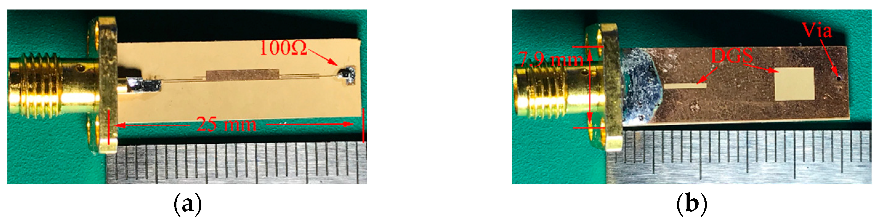
Figure 12.
Proposed UWB filtering impedance transformer (from 50 Ω to 25 Ω). Substrate: RT/Duroid 6010 with εr = 10.8 and thickness = 0.254 mm.
Figure 12.
Proposed UWB filtering impedance transformer (from 50 Ω to 25 Ω). Substrate: RT/Duroid 6010 with εr = 10.8 and thickness = 0.254 mm.

Figure 13.
Simulated S-parameters (W4 = 0 mm, W2 = 0 mm, 0.7 mm, and 1.1 mm): (a) S11; (b) S21.

Figure 14.
Simulated S-parameters (W2 = 1.1 mm, W4 = 0 mm, 0.6 mm, and 0.8 mm).

Figure 15.
E field and H field of impedance transformers (from 50 Ω to 25 Ω): (a) 2 GHz; (b) 6.85 GHz; (c) 12 GHz.
Figure 15.
E field and H field of impedance transformers (from 50 Ω to 25 Ω): (a) 2 GHz; (b) 6.85 GHz; (c) 12 GHz.
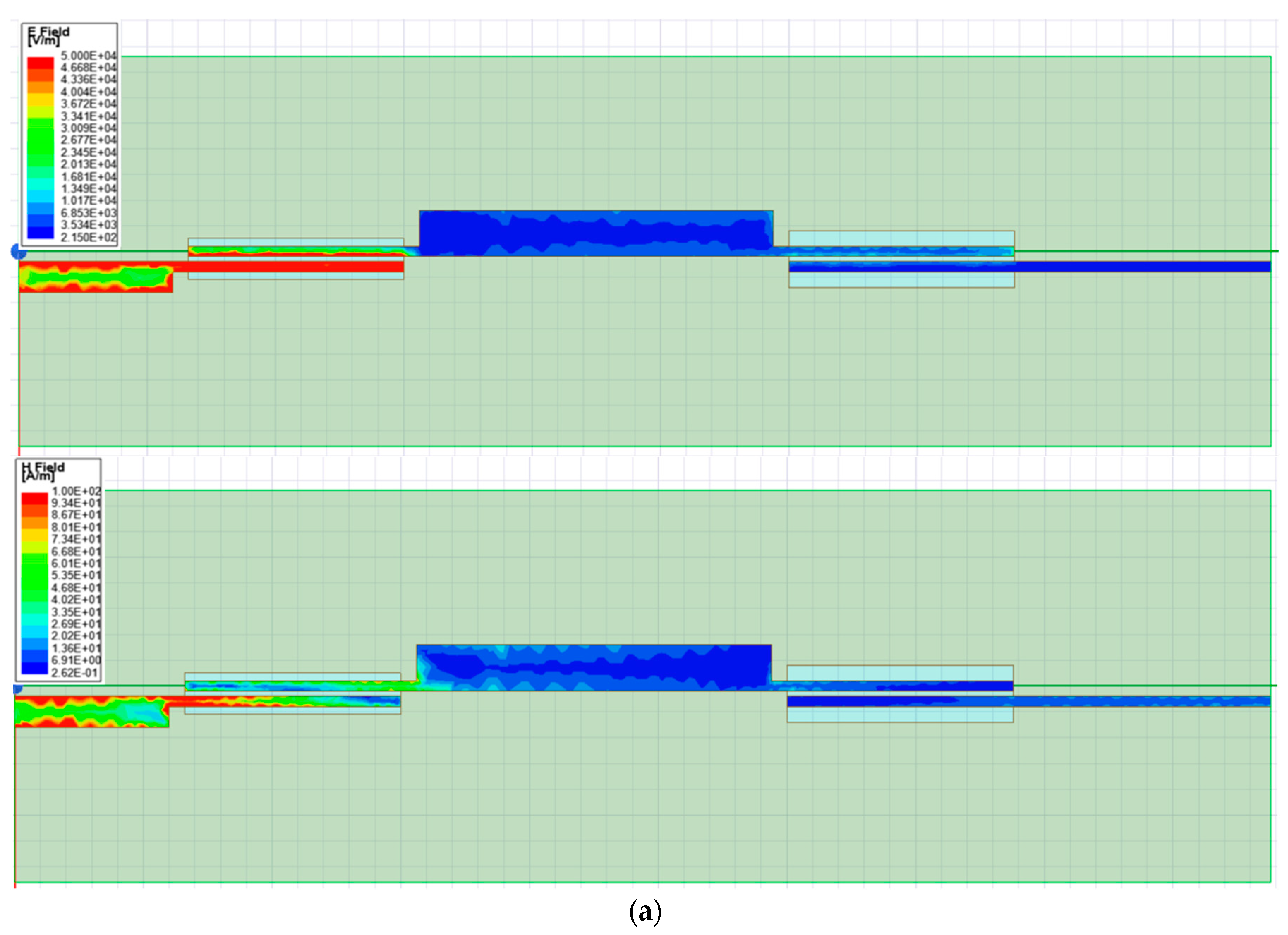

Figure 16.
Simulated and measured S-parameters of designed filtering UWB impedance transformer (from 50 Ω to 25 Ω).
Figure 16.
Simulated and measured S-parameters of designed filtering UWB impedance transformer (from 50 Ω to 25 Ω).
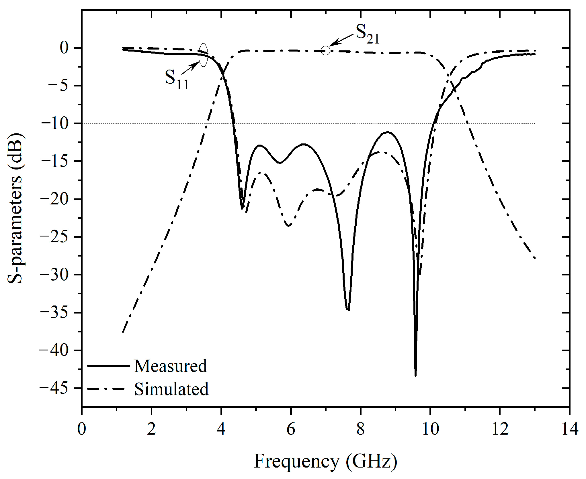
Figure 17.
Photographs of the fabricated filtering UWB impedance transformer (from 50 Ω to 25 Ω): (a) Top view; (b) Bottom view.
Figure 17.
Photographs of the fabricated filtering UWB impedance transformer (from 50 Ω to 25 Ω): (a) Top view; (b) Bottom view.
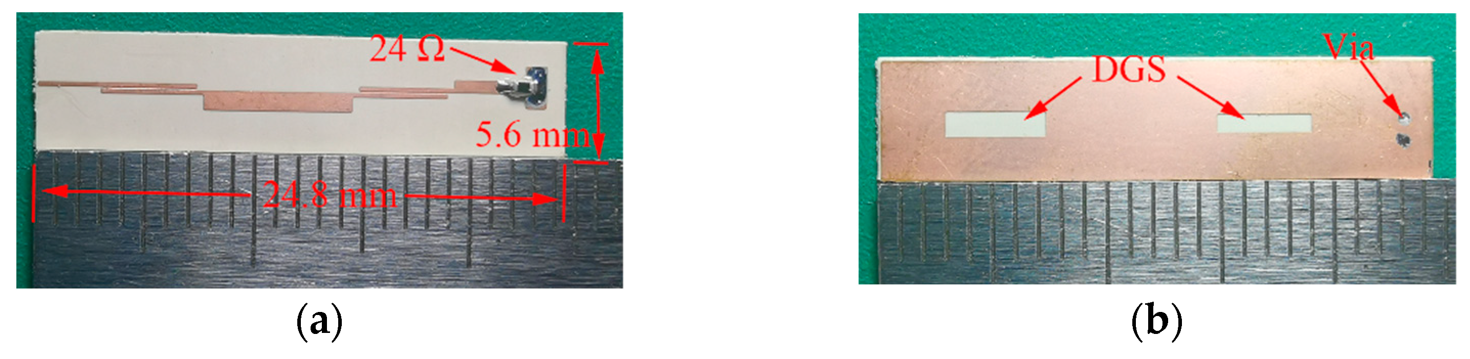
Figure 18.
UWB filtering power divider based on transformers from 50 Ω to 100 Ω. Substrate: RT/Duroid 6010 with εr = 10.8 and thickness = 1.27 mm.
Figure 18.
UWB filtering power divider based on transformers from 50 Ω to 100 Ω. Substrate: RT/Duroid 6010 with εr = 10.8 and thickness = 1.27 mm.
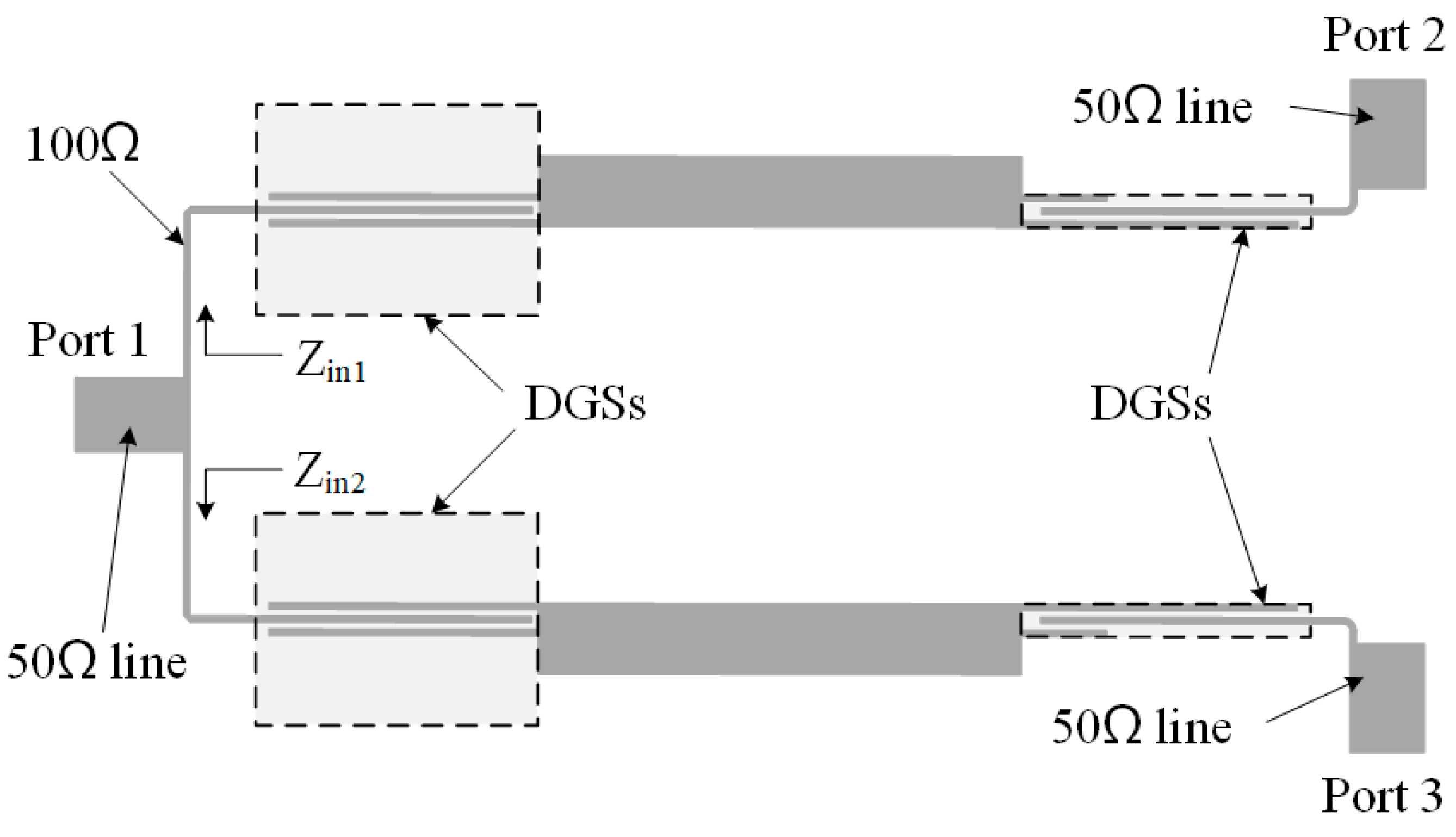
Figure 19.
Simulated S-parameters of designed filtering UWB power divider (from 50 Ω to 100 Ω).
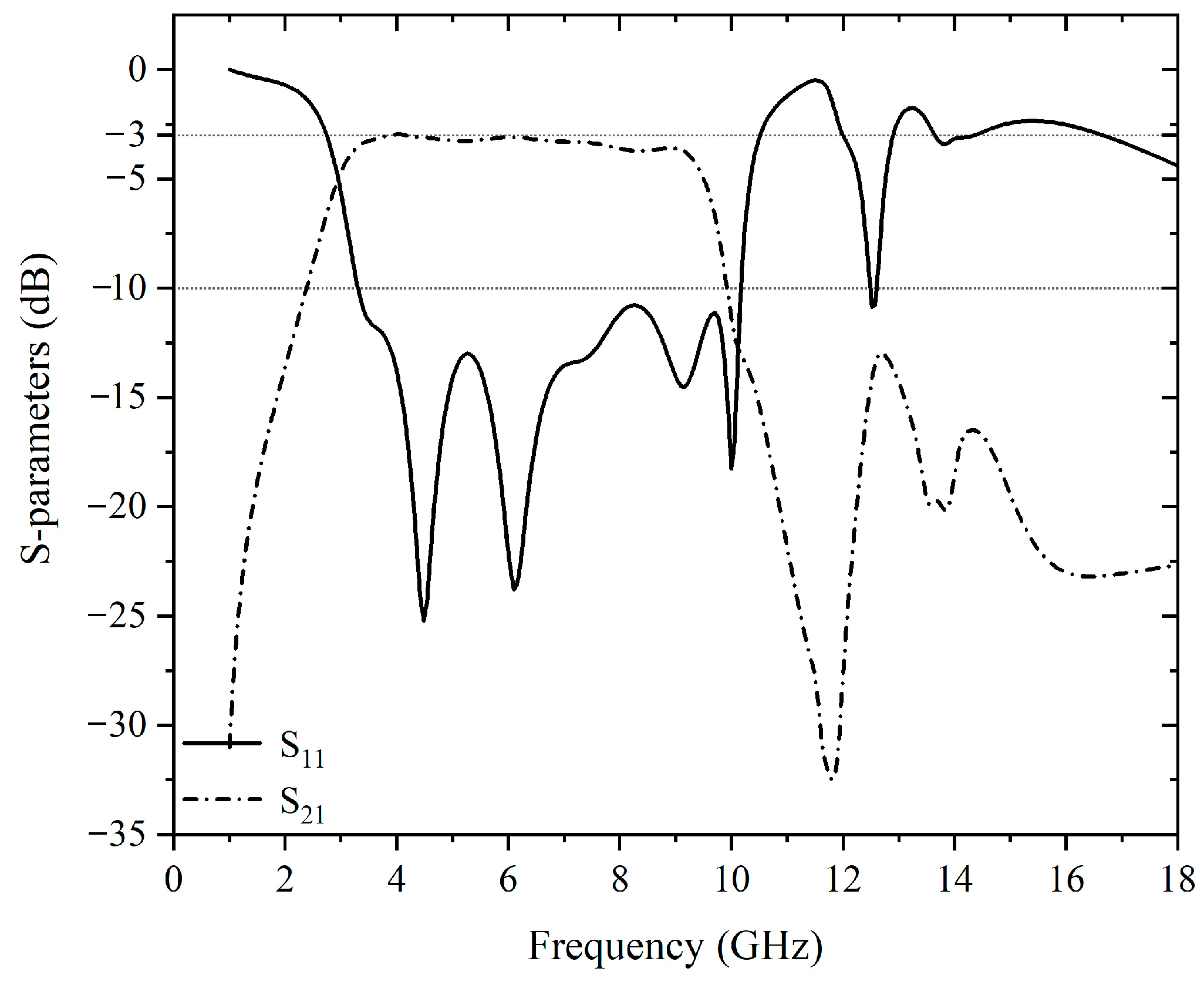
Figure 20.
Simulated and measured S-parameters of designed filtering UWB power divider (from 50 Ω to 100 Ω).
Figure 20.
Simulated and measured S-parameters of designed filtering UWB power divider (from 50 Ω to 100 Ω).

Figure 21.
Simulated and measured group delay of designed filtering UWB power divider (from 50 Ω to 100 Ω, between port 1 and port 2).
Figure 21.
Simulated and measured group delay of designed filtering UWB power divider (from 50 Ω to 100 Ω, between port 1 and port 2).

Figure 22.
Photographs of the fabricated filtering UWB power divider (from 50 Ω to 100 Ω): (a) Top view; (b) Bottom view.
Figure 22.
Photographs of the fabricated filtering UWB power divider (from 50 Ω to 100 Ω): (a) Top view; (b) Bottom view.
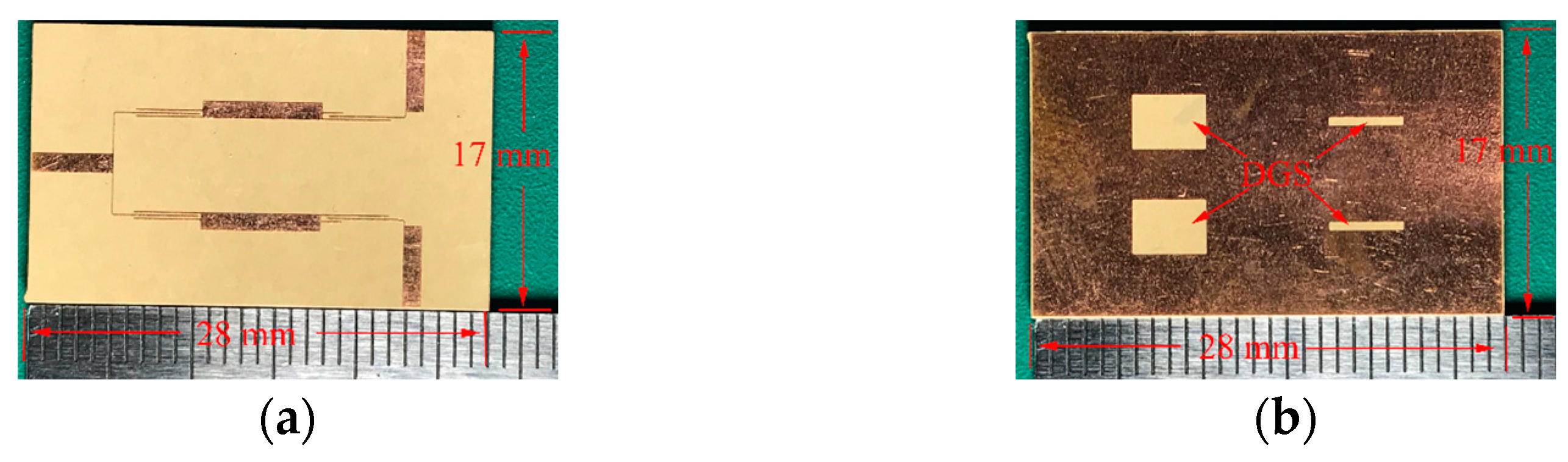
Figure 23.
UWB filtering power divider based on transformers from 50 Ω to 25 Ω. Substrate: RT/Duroid 6010 with εr = 10.8 and thickness = 0.254 mm.
Figure 23.
UWB filtering power divider based on transformers from 50 Ω to 25 Ω. Substrate: RT/Duroid 6010 with εr = 10.8 and thickness = 0.254 mm.

Figure 24.
Simulated S-parameters of designed filtering UWB power divider (from 50 Ω to 25 Ω).

Figure 25.
Simulated and measured S-parameters of designed filtering UWB power divider (from 50 Ω to 25 Ω).
Figure 25.
Simulated and measured S-parameters of designed filtering UWB power divider (from 50 Ω to 25 Ω).

Figure 26.
Simulated and measured group delay of designed filtering UWB power divider (from 50 Ω to 25 Ω, between port 1 and port 2).
Figure 26.
Simulated and measured group delay of designed filtering UWB power divider (from 50 Ω to 25 Ω, between port 1 and port 2).
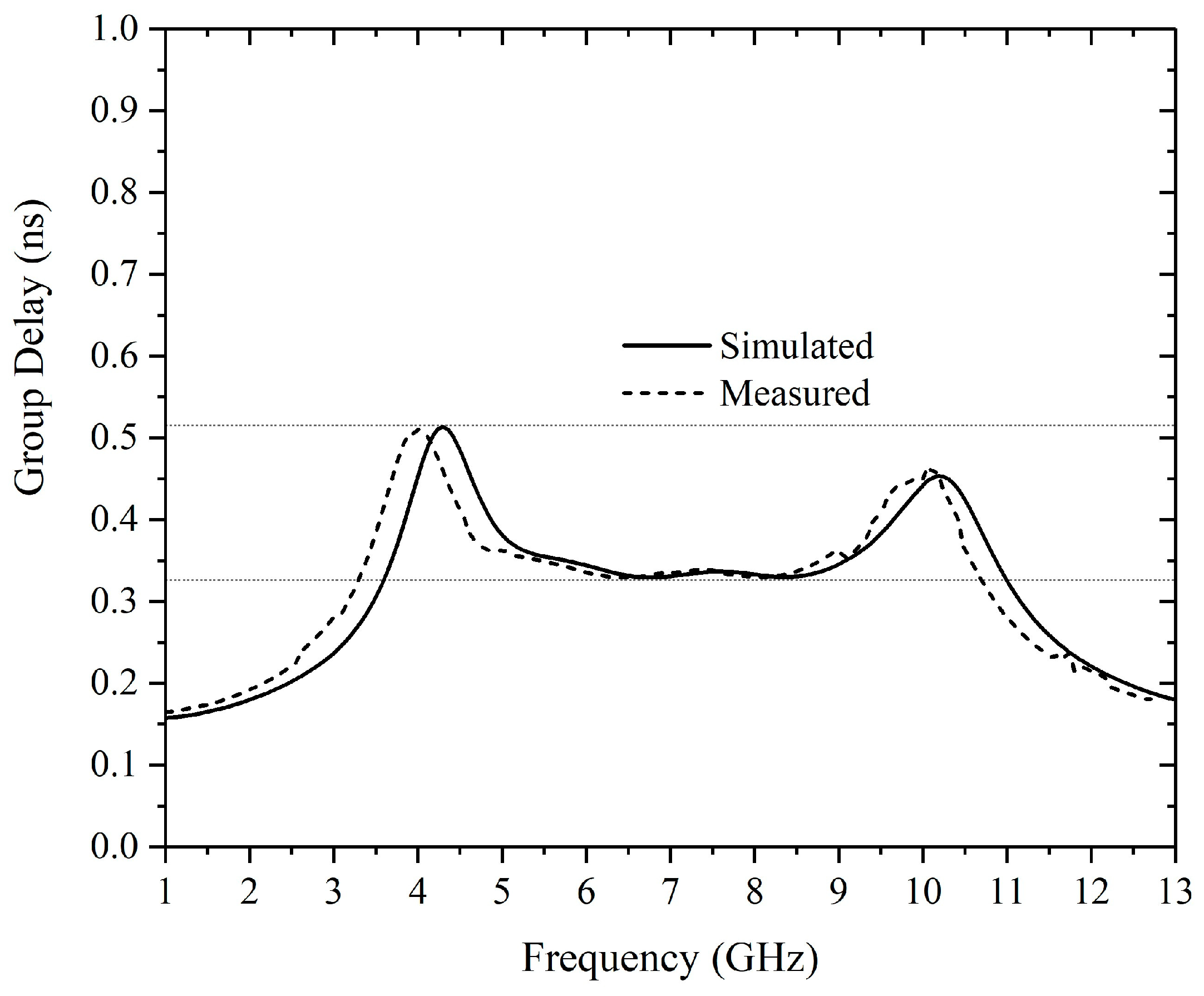
Figure 27.
Photographs of the fabricated filtering UWB power divider (from 50 Ω to 25 Ω): (a) Top view; (b) Bottom view.
Figure 27.
Photographs of the fabricated filtering UWB power divider (from 50 Ω to 25 Ω): (a) Top view; (b) Bottom view.


Table 1.
Dimensions of the UWB filtering impedance transformers (from 50 Ω to 100 Ω).
| L0 | L1 | L2 | L3 | L4 | L5 | L6 | L7 | L8 |
| 4.4 | 4.2 | 3.9 | 1.3 | 7.34 | 4.3 | 4.1 | 4.1 | 4 |
| W0 | W1 | W2 | W3 | W4 | S | unit: mm | ||
| 0.1 | 1.16 | 0.5 | 1.08 | 3.4 | 0.1 | |||
Table 2.
Dimensions of the UWB filtering impedance transformers (from 50 Ω to 25 Ω).
| L0 | L1 | L2 | L3 | L4 | S | |||
| 4.4 | 4.7 | 6.9 | 4.2 | 4.5 | 0.1 | |||
| W0 | W1 | W2 | W3 | W4 | W5 | unit: mm | ||
| 0.2 | 0.2 | 1.1 | 0.9 | 0.8 | 0.6 | |||
Table 3.
Comparison between several UWB power dividers.
| Ref. | Passband (GHz) | RL (dB) | IL (dB) | Sizes (mm × mm) | Filtering |
|---|---|---|---|---|---|
| [8] | 3.1–10.6 | 10 | 3.5 | 30 × 40 (2.3λ × 3λ) | N/A |
| [9] | 3.1–10.6 | 10 | 3.5 | 16 × 18 (1.2λ × 1.3λ) | N/A |
| [10] | 3.1–10.6 | 10 | 4–5 | 20 × 43 (1.5λ × 3.2λ) | N/A |
| [11] | 2.8–10.6 | 10 | 3.5 | 23 × 27 (1.7λ × 2λ) | N/A |
| This Work | 4–10 | >11 | 3.6–4.5 | 17 × 28 (1.2λ × 2.1λ) | UWB filtering |
| 4–10.6 | >12 | 3.5–4.4 | 6.6 × 23.6 (0.5λ × 1.74λ) | UWB filtering |
Disclaimer/Publisher’s Note: The statements, opinions and data contained in all publications are solely those of the individual author(s) and contributor(s) and not of MDPI and/or the editor(s). MDPI and/or the editor(s) disclaim responsibility for any injury to people or property resulting from any ideas, methods, instructions or products referred to in the content. |
© 2023 by the authors. Licensee MDPI, Basel, Switzerland. This article is an open access article distributed under the terms and conditions of the Creative Commons Attribution (CC BY) license (https://creativecommons.org/licenses/by/4.0/).
Share and Cite
MDPI and ACS Style
Cao, Z.; Liu, Y.; Liang, C.; Majid, I. Design of UWB Filtering Impedance Transformers and Power Dividers Using Stepped-Impedance Resonators. Electronics 2023, 12, 2800. https://doi.org/10.3390/electronics12132800
AMA Style
Cao Z, Liu Y, Liang C, Majid I. Design of UWB Filtering Impedance Transformers and Power Dividers Using Stepped-Impedance Resonators. Electronics. 2023; 12(13):2800. https://doi.org/10.3390/electronics12132800
Chicago/Turabian StyleCao, Ziheng, Yun Liu, Chen Liang, and Irfan Majid. 2023. "Design of UWB Filtering Impedance Transformers and Power Dividers Using Stepped-Impedance Resonators" Electronics 12, no. 13: 2800. https://doi.org/10.3390/electronics12132800
Note that from the first issue of 2016, this journal uses article numbers instead of page numbers. See further details here.