
Frequency-Based Sensor Interface with Dynamic Offset Compensation


1
Department of Electrical and Computer Engineering, Addis Ababa Institute of Technology, Addis Ababa University, Addis Ababa 1178, Ethiopia
2
Department of Electrical Engineering, Faculty of Engineering Technology, Katholieke Universiteit Leuven, 3000 Leuven, Belgium
*
Author to whom correspondence should be addressed.
Electronics 2023, 12(7), 1524; https://doi.org/10.3390/electronics12071524
Submission received: 28 February 2023
/
Revised: 21 March 2023
/
Accepted: 22 March 2023
/
Published: 23 March 2023
(This article belongs to the Special Issue Radiation Tolerant Electronics, Volume III)
Abstract
:Sensor interfaces need to be robust and accurate for many applications. This is more challenging for sensor systems operating in radiation environments because the mismatch between components grows as a result of the absorbed total ionizing dose (TID). In frequency-based sensor interfaces, the frequency drift of the voltage-controlled oscillator (VCO) can create dynamic output offset, gain, and linearity errors unless a calibration algorithm is included. In this paper, a digital intensive dynamic offset cancelation technique is proposed for an open loop VCO-based sensor to digital converter, which is achieved by making periodic adjustments to the average center biasing voltage of one of the VCOs in a differential architecture, in effect to make their center frequencies match. A simulation of the behavioral model of the proposed architecture was developed and hardware implementation of the whole system was performed on an FPGA by emulating, with digital modules, the characteristics of the two VCO outputs modulated with differential inputs. The results showed that the output offset error was reduced from around 5% to 0.1% for a relative oscillators’ drift close to 10% of the tuning range, and the SNDR is relatively maintained when subjected to variable relative VCO drifts.
1. Introduction
The accuracy and robustness of a sensor system are of high importance, especially for applications like biomedical instruments, aerospace devices, environmental monitoring, and automotive electronics. The accuracy of a sensor system depends on both the quality of the sensor and the design of the interfacing circuitry. The output of a good sensor may be distorted by a poorly designed sensor interface circuit, which finally degrades the accuracy of the overall system. The types of errors introduced by the interfacing elements can be static or dynamic in nature. The static errors are mainly due to fixed component non-idealities and are relatively easier and simpler to calibrate because they can be measured in advance. However, dynamic errors such as those resulting from variable TID of the surrounding are more difficult to detect, measure, and compensate for.
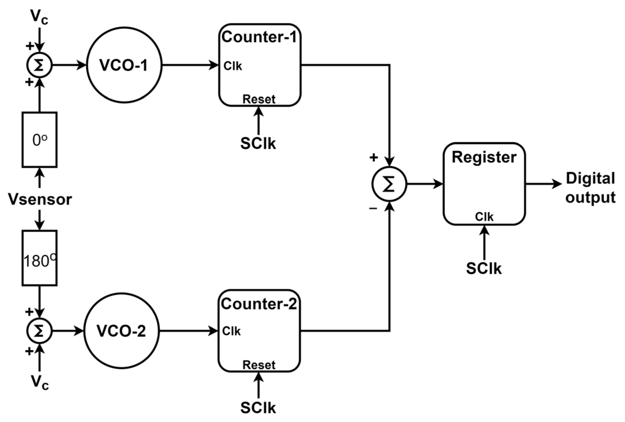
VCO-based sensor to digital converters have been under investigation for their highly digital-intensive architecture, low area, low power, and high scalability [1]. Time-/frequency-based architectures are more suited for digital implementations, which make most of the components less sensitive to process, voltage, and temperature (PVT) variations and variable TID. This leaves us with the VCO, which is a highly sensitive block. It has been reported that VCOs experience a drift in frequency when operated in radiation environments like deep space and nuclear environments, which is related to the amount of TID they absorb [2,3]. A frequency increase of around 30 MHz throughout the linear operating region of a CMOS-based ring VCO is reported in [4] for a TID level of 300 krad (SiO2). This offset drift accounts for almost 14% of the total operating range. This indicates that the center frequency of a VCO operating in a radiation environment shifts significantly depending on the level of the absorbed TID by the VCO, which in turn leads to a dynamic offset error at the system output. A differential architecture shown in Figure 1 is usually adapted to suppress common mode VCO variations owing to various environmental factors, where Vc is the common dc center biasing voltage, Vsensor is the measured input sensor voltage, and SClk is the sampling clock. However, the operation of these converters in harsh environments can result in a variable level of TID absorbed by the two VCOs at any given time. This results in a changing mismatch between the center frequencies of the two VCOs, which finally creates a dynamic offset error in the digital output that can no longer be compensated for by the differential architecture only.
Auto-zeroing and chopping are dynamic offset cancellation techniques well known for their wide application in analog amplifiers [5,6]. Auto-zeroing involves sampling and storing the offset voltage on a capacitor at one phase and making compensation in the subsequent phase. On the other hand, chopping involves modulation of the signal to a higher frequency and then demodulating it back to the baseband after it has passed through the offset-causing blocks. In such a way, the signal can be recovered and the offset that is up-converted to a higher frequency can be filtered out. These concepts are also exploited for amplitude-based ADCs where the comparator is the main source of an offset error [7,8]. In all of the above techniques, the information of the processed signal is found in the amplitude of the signal. When it comes to frequency-based ADCs, where the information is found in the frequency of signals, new techniques are required including adapting the analog techniques to the digital domain.
PLL-based sensor readout systems, which work on the principle of relative comparison between two VCOs, were investigated for their potential to cancel a drift due to environmental factors, usually temperature effects [1,9,10,11]. Here, one of the VCOs tries to lock to the other sensor-modulated VCO using a digital phase detector/filter. Therefore, if the two VCOs drift by equal amounts, then there will be no significant change in the input of the VCO in the loop from which the digital output is derived. Nevertheless, these structures assume that external impacts would be similar to both VCOs. Thus, the accuracy of such systems highly depends on the matching between the two VCOs.
Time domain chopping techniques combined with VCO tuning were applied to PLL-based sensor to digital converters to address the effect of dynamic offsets in [12,13,14]. The VCO tuning technique is aimed at reducing the residual offset after the chopping process. Here, the chopping frequency imposes some restrictions on the sampling frequency, which places a limitation on the maximum sensor bandwidth.
A PLL-based converter that uses two cycles, one for determining the offset calibration parameters and one for signal conversion, is proposed in [15]. Here, a set of calibration bits is determined in one cycle, which modulates the delay of each stage of the ring oscillators, in effect canceling the offset during the conversion cycle. This requires applying these sets of biasing circuitry, which are equal to the number of calibration bits, to every delay stage of the two oscillators.
This paper proposes an open loop VCO-based sensor to digital converter with digital intensive relative average center biasing voltage control of one of the VCOs to cancel any arising dynamic offset error at the system level. The organization of the paper is as follows. In Section 2, the architecture and operation principle of the dynamic offset cancellation circuit are discussed. Behavioral simulation results and a hardware performance test of an emulated structure on an FPGA are demonstrated in Section 3. Section 4 concludes the paper.
2. Dynamic Offset Cancelation Technique
In this proposed architecture, digital intensive structures are developed to make the average center biasing voltage of VCO-2 automatically and periodically adjust itself to a voltage value corresponding to the center frequency of VCO-1. This ensures that there will be no dynamic offset error manifested at the digital output even if a variable drift occurs between the two VCOs during the operation of the converter.
There are two phases of operation, calibration (Phase-I) and conversion (Phase-II). The calibration phase is the period during which the amount of adjustment needed for the center biasing voltage of VCO-2 is determined and the conversion phase is the period during which the sensor-to-digital conversion takes place. The choice of the calibration frequency, which specifies how often the system needs the offset correction, depends on the estimation of the frequency of the occurrence of the varying offset. For example, in the case of a radiation environment, the dose rate of the operation environment can be used to decide on the design of the frequency of the offset adjustment. The maximum calibration frequency is used in this work, which is equal to the value of the sampling frequency. This can be achieved by allotting half of the sampling clock period for calibration and the other half for conversion. However, based on the assessment of the occurrence of a new offset value on the system, the frequency of the offset adjustment can be lowered. In such a case, an additional counter clocked by the sampling clock can be used in such a way that an offset calibration phase is initiated whenever the counter reaches a specific value. For example, a 4-bit counter can be used and a calibration phase can be initiated whenever the counter resets. Therefore, here, the calibration data are collected on the LUT during a zero count of the counter and the rest of the counting stages will be used for data conversion. In this case, the offset calibration frequency will be 1/16 of the sampling clock frequency. The detailed operation principles of the two phases are discussed as follows.
2.1. Calibration Phase (Phase-I)
The purpose of this calibration phase is to match the average center frequencies of the two VCOs, during which time the input sensor voltage is disconnected from the system. This can be achieved by employing the two VCOs in a phase-locked loop, where VCO-2 tries to lock itself to VCO-1 and, finally, the settling voltage of VCO-2 will be used as its center biasing voltage for the conversion period. It is known that a digital-intensive architecture would be less prone to TID effects. Besides, an energy-efficient calibration system is favored to reduce extra power overheads. Taking those considerations, during this phase, the two VCOs are connected in a closed loop system involving a D flip flop (DFF) as a single-bit phase detector and a one-bit digital to analog converter (1-bit DAC), as depicted in Figure 2. The DFF receives the output of VCO-2 at its data input and that of VCO-1 at the clock input and its output indicates whether the phase of VCO-2 is leading (binary 1) or lagging (binary 0), with respect to the phase of VCO-1. Here, VCO-1 is biased by a constant biasing voltage Vc1. The output of the D-FF is connected to both a 1-bit DAC and a look-up table (LUT). The purpose of the LUT is to store the series of DFF outputs at each clock cycle during this phase at successive locations on the LUT. The digital output of the DFF is also given to a 1-bit DAC. Based on the output of the DFF, the 1-bit DAC switches between two voltage values Va and Vb, which represent two levels of voltages between which the required average center biasing voltage of VCO-2 is expected to lie. After the end of the calibration period, the average value of the DAC output, , would be equal to the required center biasing voltage of VCO-2, which compensates for the drift of its center frequency relative to VCO-1, thereby eliminating any offset output during the conversion phase.
Mathematically, the required average center biasing voltage of VCO-2, , can be expressed as (1), where and are the number of ones and zeros, respectively, coming from the DFF output every clock cycle during Phase-I.
The series of DFF outputs at each clock cycle are stored at successive locations on the LUT, as designated in Figure 2. The aim is that it can be used to drive the same one-bit DAC later in the conversion phase to give an average estimate of the newly adjusted center biasing voltage for VCO-2. As one new bit is written every cycle of VCO-1 output, the maximum possible size of the LUT, , is defined by the product of the value of the center frequency of VCO-1, , and the period of the calibration phase, , as given in (2).
Depending on the level of accuracy required, any size of LUT that is less than can be used, whose impact is demonstrated in Section 3. If the size of the LUT is bits, then Equation (1) can be rewritten as (3), where n is the number of ones in the LUT.
2.2. Conversion Phase (Phase-II)
The operation during Phase-II is the conversion of the available input sensor voltage to a digital value using an open loop differential architecture, as illustrated in Figure 3. VCO-1 is center biased with a constant biasing voltage, Vc1. At every cycle of a reference oscillator, Ref, the successive bits stored on the LUT during Phase-I drive the 1-bit DAC to provide the center biasing voltage of VCO-2, Vc2.
The two counters, Counter-1 and Counter-2, count the edges of VCO-1 and VCO-2, respectively, for a duration allotted to Phase-II. The contents of the two counters are sampled by the corresponding registers (Register-1 and Register-2) at the rising/falling edges of the sampling clock (SClk) and subtracted to deliver the final digital output, which is expected to be free from an offset. A non-linearity calibration (NLC) block follows to suppress the major harmonic contents of the digital output that arose as a result of the nonlinearity of the VCOs.
3. Results
3.1. Simulation Results
To test the performance of the dynamic offset compensation structure discussed in Section 2, a behavioral simulation is conducted and the variation in its performance with some critical parameters is analyzed. The tuning curves of the VCOs can be approximated using a polynomial-regression-based model [16], as given in (4). The frequencies of VCO-1 and VCO-2, and respectively, are modeled with third-order polynomials as shown in (4) and (5), with coefficients , , , and .
As offset error shifts the entire transfer function by the same value, two identical VCOs with matching coefficients are assumed, which develop a relative dynamic offset drift, , between them through time. The phase noise of the each VCO is incorporated by including an equivalent voltage noise, , at the input of the VCO, , as in (6).
The parameters used in the simulation are listed in Table 1. Theoretically, the offset cancellation algorithm can be applied to any range of VCO frequencies. Here, a tuning sensitivity per peak-to-peak input voltage of 100 MHz/ is used, as it is approximately the maximum range of frequency that can be comfortably used for the digital emulation of the VCO on the ZYBO FPGA (in Section 3.2) without causing timing issues. Owing to the non-linearity of the VCO, the achievable effective number of bits of open loop VCO-based ADCs is limited to 6 to 7 bits [17], which corresponds to a major distortion figure of around −40 dBc. The tuning sensitivity value and the distortion figure are then translated into polynomial coefficients as a function of and adjusted to be suited for digital implementation, as shown in Table 1. The initial center frequency of the VCOs, Fc, is 100 MHz. A sinusoidal signal with a frequency, Fin, of 5 kHz is used as an input. The output sampling frequency, Fclk_samp, is around 98 kHz and a bandwidth of 20 kHz is assumed, which is quite enough for most sensor applications.
The parameters of particular interest are the size of the LUT, , and the normalized biasing range of , , which is given as (7):
To characterize the impact of the relative offset in terms of the signal to noise and distortion ratio (SNDR), is modeled as random frequency uniformly distributed between two bounds to where designates the maximum magnitude of the relative VCO frequency drift.
An offline non-linearity correction block is designed with a look-up table plus a linear interpolation method [18]. Here, 64 points are stored in memory and the rest of the corrected outputs are evaluated with linear interpolation. Figure 4 shows the power spectral density of the offset compensation architecture for R = 0.125, L = 512, and = 3 MHz. It is shown that the second harmonic distortion is suppressed by the differential architecture and the remaining third harmonic distortion is reduced by the NLC block, which resulted in an output SNDR of around 56 dB (ENOB of around 9 bits). This shows that an offline calibration can be enough if any prior offset errors are effectively compensated.
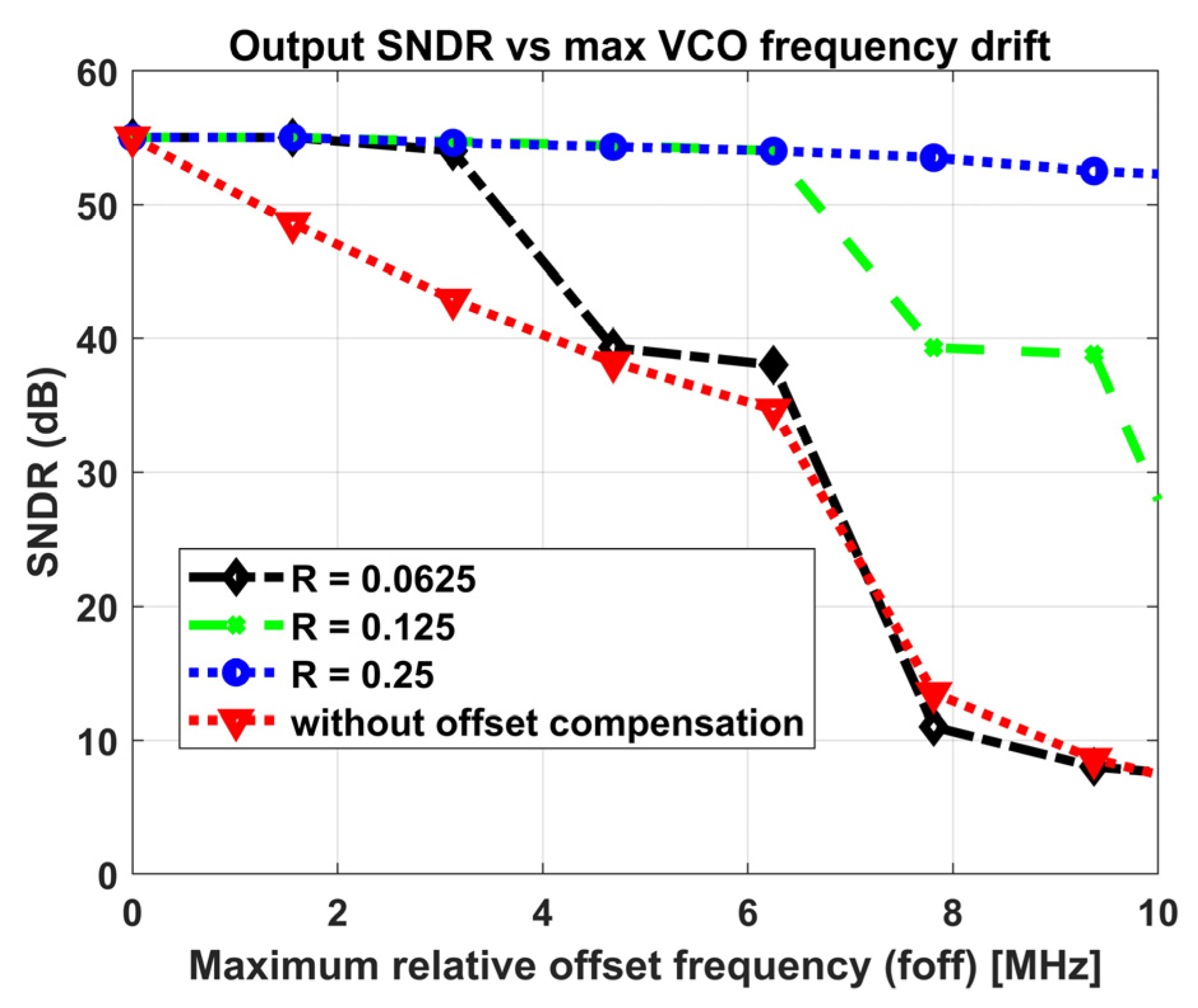
The variation in the output SNDR with the magnitude of the maximum relative offset frequency of the two VCOs () is depicted in Figure 5 for the architectures with and without offset compensation. For the architecture without offset cancelation, the SNDR degrades sharply whenever the relative drift between the two VCOs grows.
The SNDR for the architecture with the offset compensation is plotted for three values of R. For R = 0.0625, the SNDR shows a sharp decline after a 3 MHz relative VCO drift, whereas for R = 0.125, the cut-off point extends up to a relative drift of around 7 MHz. For R = 0.25, the structure relatively sustains its SNDR and no sharp degradation point occurs in the whole range of the plot. Here, the cut-off points are related to the maximum relative offset for which the system can compensate. It can also be observed that the values of the cut-off points are related to the values of R, which indicate that the choice of the value of R depends on the estimate of the expected maximum relative offset drift between the two VCOs.
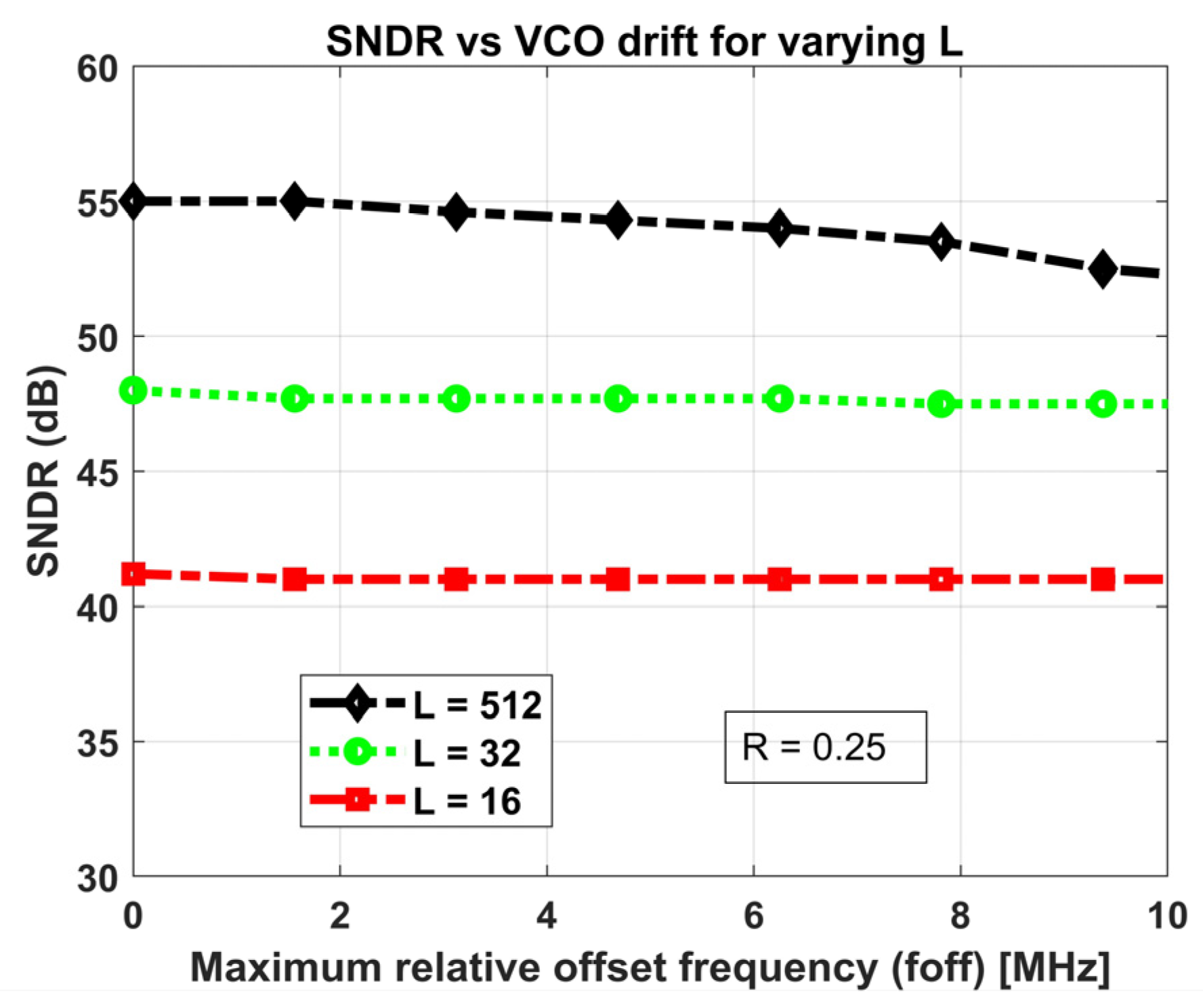
The impact of varying the size of the LUT, L, on the output SNDR is shown in Figure 6. In Figure 6a, an R value of 0.125 is used and the plot of output SNDR almost overlaps for L values of 512 and 128 bits. A clear distinction starts to appear for L values less than 64 bits, after which the SNDR starts to degrade. In Figure 6b, an R value of 0.25 is used and the plot of output SNDR starts to make a visible difference for L values less than 128 bits and degrades after that. From this, we can observe that L represents the level of resolution we achieve for the center biasing voltage of VCO-2 in the normalized range of R. The voltage resolution of the biasing voltage of VCO-2 normalized by , , can be expressed as (8).
So, the higher the value of R, the poorer the voltage resolution for a fixed L. Alternatively, the lower the value of L, the poorer the voltage resolution for a fixed R. The normalized input voltage resolution, , for the whole system can be represented as (9), where is the effective number of bits (ENOB) of the digital output.
The choice of lower values of L starts to affect the SNDR of the final output whenever approaches . If passes beyond , the output SNDR starts to degrade because, now, would be the limiting factor.
3.2. Digital Implementation Results
To measure the dynamic performance of an implemented structure, an FPGA implementation of the whole system was developed by emulating, with digital modules, the major characteristics of the outputs of the two VCOs that are modulated by differential sinusoidal input voltages, which is briefly explained in the next section.
3.2.1. Hardware Emulation of Sine-Input-Modulated VCO
By assuming a sinusoidal input voltage, the input-modulated non-linear VCOs are emulated by cascading a digital sinusoidal wave generator and a numerically controlled oscillator, as shown in Figure 7. The digital sinusoidal wave generator generates two sine waves ( and ) with second and third harmonic contents, as expressed in (10) and (11), where and are coefficients that specify the levels of the second and third harmonics, respectively.
Sensor frequency control word (SFCW) is a number corresponding to the frequency of the input sensor voltage. Then, at every cycle of the input clock, Clk_Sin, the phase accumulator register outputs a digital ramp phase value, , whose frequency is proportional to SFCW. Phase-to-sine/-cosine converters designed with a sixteen-stage CORDIC algorithm are used to convert the digital ramp phases to digital sinusoidal waves. The square and cube terms in (10) & (11) are rewritten as in (12) & (13) respectively, and implemented in the arithmetic block of Figure 7, which are suited for an optimized hardware implementation that avoids multiplication.
If and are approximated around negative powers of two, then the multiplication and division operations in the second and third terms in 12 and 13 can be implemented using only shift operations. This means the operations in the arithmetic block of Figure 7 are only addition, subtraction, and shift operations, which greatly optimize the speed of the hardware implementation. and are then added to the respective center biasing values, d_bias1 and d_bias2, and serve as input to the two numerically controlled oscillators NCO-1 and NCO-2, respectively. The numerically controlled oscillators accumulate this input every cycle of Clk_NCO and the MSBs of these phase accumulators, V1 and V2, emulate the outputs of the two square wave VCOs modulated by differential sinusoidal input voltages.
3.2.2. LUT Implementation
The LUT is implemented with a circular shift register with write and read modes that are controlled by the level of the sampling clock, SClk, as shown in Figure 8. When SClk is low (calibration phase), the LUT will be in writing mode, where it loads the series of bits coming from the DFF phase detector (output of Mux-2) every cycle of VCO-1 (output of Mux-1). When SClk is high (calibration phase), the LUT will be in a reading mode, where it circularly shifts every cycle of Ref (output of Mux-1), thereby delivering consecutive output bits, Data_out, stored in the calibration phase. The size of the LUT, L, is the total number of DFFs in the LUT, whose maximum value is given in (2).
3.2.3. Measured Results
The architecture for the implementation of the full system is depicted in Figure 9. The two operation phases are employed using a digital multiplexer (Mux) and digitally controlled switches (SW-1 and SW-2), which are all controlled by the level of the sampling clock, SClk.
A maximum calibration frequency is assumed where half of the sampling period is used for calibration and the other half is used for the conversion process. Accordingly, Phase-I occurs when the level of the sampling clock, SClk, is low, during which the LUT will be in writing mode, the 1-bit DAC is controlled by the DFF output, and the outputs of the two digital sine wave generators are disconnected from the system. Va and Vb, which were outputs of the 1-bit DAC in Figure 3, are substituted with their digital equivalents of da and db, respectively.
Phase-II occurs when the level of SClk is high. Here, the LUT will be in reading mode and the one-bit DAC is now controlled by the successive bits read from the LUT every clock cycle of the reference oscillator, Ref. The outputs of the two digital sine wave generators are now connected to the system. The two counters, Counter-1 and Counter-2, count the edges of the VCO-1 and VCO-2 signals, respectively, for a duration of half of the sampling period, and then the output is sampled at the end of this period.
The VCO waves and the sampling clock constitute separate clock domains, which means the rising edges of one can occur independently of the other. This can lead to meta-stability issues during the sampling process, which could lead to corrupted outputs. The closer the metastable bits are to the MSB, the higher the sampling error. To avoid the possibility of such high errors, a binary to gray converter is used before sampling so that the possibility of metastable bits is reduced to less than one LSB. Then, a gray to binary code converter is used to convert it back to binary for the later subtraction process to deliver the differential output.
A 64-point offline non-linearity calibration block with linear interpolation is used to correct the distortions due to the oscillator’s non-linearity. Variable digital offset values in steps equivalent to around 1.5 MHz up to 9 MHz frequency drift are injected into the input of NCO-2 to emulate a variable relative VCO drift. The initial center frequency of the two oscillators, Fc, is 100 MHz and the sampling clock frequency, Fclk_samp, is around 98 kHz. The frequency of the sinusoidal input, Fin, is 5 kHz, whose peak-to-peak amplitude modulates the NCOs over a frequency range of 100 MHz. The distortion parameters, , are derived from Table 1, where their values are adjusted so that the multiplication operation can be digitally implemented using only shift operations.
A parallel structure without the dynamic offset cancelation system is also implemented with similar parameters to compare the performances. To measure the SNDR and fractional offset error, 8192 samples of the digital output are stored on a block RAM inside the ZYBO FPGA, which are later read and exported to Matlab for further analysis.
Figure 10 shows the variation in the measured fractional offset error with relative VCO drift for the architectures with and without offset compensation, which are measured for a zero value of the input. The fractional offset error is evaluated as the ratio of the digital output offset value to the full-scale output range expressed in percentage. The architecture without offset cancelation results in non-zero output offsets whenever a relative drift between the two VCO frequencies starts to occur and grows proportionally with it. For the architecture with the offset compensation, the fractional output offset errors are plotted for three values of R. For R = 0.0625, the system cancels up to around ±3 MHz relative drifts, whereas for R = 0.125, the offset cancelation range extends up to around ±6 MHz. For R = 0.25, the structure compensates for any offset in the whole plot. Here, it can be observed that the output offset error is reduced from around 5% to 0.1% for a relative drift of the oscillators, which is close to 10% of the tuning range.
The dynamic performance of the system is assessed in terms of the output SNDR by turning on the digital sine wave generator and applying a variable relative offset drift, as depicted in Figure 9. Similar sharp corners to those of Figure 10 can be observed on the plot of the variation of the measured output SNDR with relative VCO drift in Figure 11. Similar to the simulation results in Section 3.1, the system sustains its output SNDR until a certain relative frequency drift value, after which the system fails to correct further offset values. The range of frequency drift up to which the system continues to correct the offset is decided by the value of R. It is also demonstrated that the offline non-linearity correction scheme can be sufficient as long as any appearing dynamic VCO frequency offsets are canceled before the calibration block.
The impact of varying the size of the LUT, L, on the measured output SNDR after non-linearity calibration is shown in Figure 12. Only values of L that show a clear distinction in the measured SNDR are plotted. Here, we can also observe that the SNDR of the digital output can be degraded when the voltage resolution of the average biasing voltage of VCO-2, expressed in (8), is higher than that of the input voltage resolution of the system expressed in (9).
A performance comparison of this work with prior works related to offset reduction is presented in Table 2. The techniques involve either chopping, two-phase calibrations, or a combination of the two. The results of the proposed technique in this work show a good offset reduction with a relatively higher bandwidth. It can be seen that the choice of both the architecture and offset reduction technique have an impact on the applicable bandwidth. It is known that open-loop architectures are favored for high-speed applications over their closed-loop counterparts. On top of that, the restriction of the applicable bandwidth in chopping systems limits the application of the techniques, which use both closed loop and chopping to low bandwidth applications like resistive sensor interfaces.
Given the open-loop architecture of the presented method in this work, its speed can further be improved if VCOs with higher center frequencies are used together with higher sampling frequencies. This preserves in (2) and maintain the resolution of the center biasing voltage. In such a way, it is possible to perform the two phases faster, which can make it a good alternative for even higher-speed applications.
4. Conclusions
Sensor interfaces operating in radiation environments suffer from performance degradation as a result of varying levels of absorbed total ionizing dose. One of these performance degradations in frequency-based sensor-to-digital converters is an output offset error, which is caused by the dynamic mismatch between the center frequencies of the two VCOs. In this work, a digital intensive architecture was presented that can successfully suppress any variable output offset error, by periodically calibrating the average center biasing voltage of one of the VCOs. This average center biasing voltage was employed by interpolating it from two fixed bias values, where the interpolation data are obtained during the calibration phase. It is demonstrated that the range of these two fixed bias values determines the range of VCO frequency drift that the system can correct. It can also be concluded that the voltage resolution between these two fixed values should be lower than that of the converter’s voltage resolution so that it would not be the limiting factor for the SNDR of the digital output.
Author Contributions
Conceptualization, M.B.Z.; methodology, M.B.Z.; software, M.B.Z.; validation, M.B.Z., G.A. and P.L.; formal analysis, M.B.Z.; investigation, M.B.Z.; resources, M.B.Z., V.D.S. and P.L.; writing—original draft preparation, M.B.Z.; writing—review and editing, M.B.Z., G.A. and P.L.; supervision, P.L., G.A. and V.D.S.; project administration, P.L., G.A. and V.D.S. All authors have read and agreed to the published version of the manuscript.
Funding
This research was supported by the Home-Grown PhD Program (HGPP) funded by the Ethiopian Ministry of Education.
Data Availability Statement
Not applicable.
Conflicts of Interest
The authors declare no conflict of interest.
References
- Gielen, G.; Van Rethy, J.; Marin, J.; Shulaker, M.M.; Hills, G.; Wong, H.S.P.; Mitra, S. Time-based sensor interface circuits in CMOS and carbon nanotube technologies. IEEE TCAS-I 2016, 63, 577–586. [Google Scholar] [CrossRef]
- Li, Z.; Elash, C.J.; Jin, C.; Chen, L.; Xing, J.; Yang, Z.; Shi, S. Comparison of Total Ionizing Dose Effects in 22-nm and 28-nm FD SOI Technologies. Electronics 2022, 11, 1757. [Google Scholar] [CrossRef]
- Prinzie, J.; Christiansen, J.; Moreira, P.; Steyaert, M.; Leroux, P. Comparison of a 65 nm CMOS Ring- and LC-Oscillator Based PLL in Terms of TID and SEU Sensitivity. IEEE Trans. Nucl. Sci. 2017, 64, 245–252. [Google Scholar] [CrossRef] [Green Version]
- Patel, B.; Joplin, M.; Boggs, R.C.; Reising, D.R.; McCurdy, M.W.; Massengill, L.W.; Loveless, T.D. Ionizing Radiation Effects Spectroscopy for Analysis of Total-Ionizing Dose Degradation in RF Circuits. IEEE Trans. Nucl. Sci. 2019, 66, 61–68. [Google Scholar] [CrossRef]
- Behzad, R. Design of Analog CMOS Integrated Circuits, 3rd ed.; McGraw-Hill: New York, NY, USA, 2001; pp. 598–604. ISBN 978-0-07-252493-2. [Google Scholar]
- Wu, R.; Huijsing, J.; Makinwa, K. Dynamic Offset Cancellation Techniques for Operational Amplifiers. In Precision Instrumentation Amplifiers and Read-Out Integrated Circuits; Springer: New York, NY, USA, 2013; pp. 21–49. ISBN 978-1-4614-3730-7. [Google Scholar]
- Gu, W.; Wu, Y.; Ye, F.; Ren, J. A Single-Ended 10-Bit 200 KS/s 607 ΜW SAR ADC with an Auto-Zeroing Offset Cancellation Technique. J. Semicond. 2015, 36, 105006. [Google Scholar] [CrossRef]
- Figueiredo, P.; Vital, J. Offset Reduction Techniques in Highspeed Analog-to-Digital Converters: Analysis, Design and Tradeoffs; Springer: Berlin/Heidelberg, Germany, 2009; pp. 261–285. ISBN 978-1-4020-9715-7. [Google Scholar]
- Van Rethy, J.; Danneels, H.; Gielen, G. Scalable Bang–Bang Phase-Locked-Loop-based integrated sensor interfaces. Microelectron. J. 2014, 45, 1641–1647. [Google Scholar] [CrossRef]
- Van Rethy, J.; Danneels, H.; De Smedt, V.; Dehaene, W.; Gielen, G.E. Supply-noise-resilient design of a BBPLL-based force-balanced wheatstone bridge interface in 130-nm CMOS. IEEE J. Solid-State Circuits 2013, 48, 2618–2627. [Google Scholar] [CrossRef]
- Danneels, H.; Piette, F.; De Smedt, V.; Dehaene, W.; Gielen, G. A Novel, PLL-Based Frequency-to-Digital Conversion Mechanism for Sensor Interfaces. Sens. Actuators A Phys. 2011, 172, 220–227. [Google Scholar] [CrossRef]
- Marin, J.; Van Rethy, J.; Vergauwen, J.; Gielen, G. Digital-domain chopping technique for high-resolution PLL-based sensor interfaces. Sens. Actuators A Phys. 2016, 249, 294–302. [Google Scholar] [CrossRef]
- Marin, J.; Sacco, E.; Vergauwen, J.; Gielen, G. Modeling and Analysis of Drift-Cancellation Techniques for Time-Based Integrated Resistive Sensor Interfaces. IEEE Trans. Compon. Packag. Manuf. Technol. 2018, 8, 1203–1212. [Google Scholar] [CrossRef]
- Marin, J.; Sacco, E.; Vergauwen, J.; Gielen, G. A Single-Temperature-Calibration 0.18-Μm CMOS Time-Based Resistive Sensor Interface with Low Drift over a −40 °C to 175 °C Temperature Range. In Proceedings of the ESSCIRC 2018—IEEE 44th European Solid State Circuits Conference (ESSCIRC), Dresden, Germany, 3–6 September 2018; pp. 330–333. [Google Scholar]
- Danneels, H.; Van Rethy, J.; Vergauwen, J.; Gielen, G. Dynamic Offset Cancellation for PLL Based Sensor Interfaces. Procedia Eng. 2012, 47, 1319–1322. [Google Scholar] [CrossRef] [Green Version]
- Yoder, S.; Ismail, M.; Khalil, W. VCO-Based Quantizers Using Frequency-to-Digital and Time-to-Digital Converters, 1st ed.; Springer: New York, NY, USA, 2011; pp. 31–33. [Google Scholar]
- Rao, S.; Reddy, K.; Young, B.; Hanumolu, P.K. A Deterministic Digital Background Calibration Technique for VCO-Based ADCs. IEEE J. Solid-State Circuits 2014, 49, 950–960. [Google Scholar] [CrossRef]
- Li, S. A Highly Digital VCO-Based ADC with Lookup-Table-Based Background Calibration. Ph.D. Thesis, Worcester Polytechnic Institute, Worcester, MA, USA, 2019. Available online: https://digitalcommons.wpi.edu/etd-dissertations/556 (accessed on 22 February 2023).
- Tu, C.-C.; Wang, Y.-K.; Lin, T.-H. A Low-Noise Area-Efficient Chopped VCO-Based CTDSM for Sensor Applications in 40-Nm CMOS. IEEE J. Solid-State Circuits 2017, 52, 2523–2532. [Google Scholar] [CrossRef]
Figure 1.
Basic architecture of a differential open-loop VCO-based sensor to digital converter.

Figure 2.
Equivalent circuit during Phase-I.

Figure 3.
Equivalent circuit during Phase-II.

Figure 4.
Power spectral density simulation of the output of the proposed offset compensation architecture before and after non-linearity correction with R = 0.125 and L = 512.
Figure 4.
Power spectral density simulation of the output of the proposed offset compensation architecture before and after non-linearity correction with R = 0.125 and L = 512.

Figure 5.
Variation in the simulated output SNDR with the magnitude of maximum relative offset frequency of the two VCOs.
Figure 5.
Variation in the simulated output SNDR with the magnitude of maximum relative offset frequency of the two VCOs.

Figure 6.
Variation in the simulated output SNDR with the magnitude of maximum relative offset frequency of the two VCOs for varying L and for (a) R = 0.125 and (b) R = 0.25.
Figure 6.
Variation in the simulated output SNDR with the magnitude of maximum relative offset frequency of the two VCOs for varying L and for (a) R = 0.125 and (b) R = 0.25.

Figure 7.
Hardware emulation of two VCOs modulated by a differential sinusoidal voltage.

Figure 8.
Implementation of the LUT.

Figure 9.
Full implemented architecture.

Figure 10.
Variation in the measured fractional offset error of the output with the magnitude of maximum relative offset frequency of the two VCOs.
Figure 10.
Variation in the measured fractional offset error of the output with the magnitude of maximum relative offset frequency of the two VCOs.

Figure 11.
Variation in the measured SNDR of the output with the magnitude of maximum relative offset frequency of the two VCOs.
Figure 11.
Variation in the measured SNDR of the output with the magnitude of maximum relative offset frequency of the two VCOs.

Figure 12.
Variation in the measured SNDR of the output with the magnitude of maximum relative offset frequency of the two VCOs for varying L.
Figure 12.
Variation in the measured SNDR of the output with the magnitude of maximum relative offset frequency of the two VCOs for varying L.


Table 1.
List of parameters used for the behavioral simulation.
| Parameters | Values |
|---|---|
| Fc (MHz) | 100 |
| Fclk_samp (kHz) | 97.7 |
| Fin (kHz) | 5 |
| Bandwidth (kHz) | 20 |
| VCO sensitivity (MHz/Vp-p) | 100 |
| VCO phase noise (dBc/Hz @ 10 kHz) | −90 |
| (MHz) | −3.03 |
| (MHz/Vp-p) | 55.1 |
| (MHz/Vp-p2) | 29.7 |
| (MHz/Vp-p3) | −6.25 |
| Non-linearity calibration points | 64 |
Table 2.
Comparison with prior works.
| Specifications | [15] | [13] | [14] | [19] | This Work | |
|---|---|---|---|---|---|---|
| Architecture | Closed-loop (PLL-based) | Closed-loop (PLL-based) | Closed-loop (PLL-based) | Open-loop differential | Open-loop differential | |
| Type | Circuit simulation | System-level simulation | CMOS imp. | CMOS imp. | FPGA imp. with VCO emulation | |
| Technology (nm) | 350 | - | 40 | 40 | - | |
| Application | General purpose | Resistive sensor | Resistive sensor | General purpose | General purpose | |
| Input frequency/Bandwidth (kHz) | - | dc/- | dc/- | 0.22/5 | 5/20 | |
| Maximum VCO mismatch (%) | - | 5 | - | - | 10 | |
| Offset reduction technique | A multi-bit adjustment of the bias of each delay element | Chopping | Chopping + VCO tuning | Chopping + VCO tuning | Chopping | LUT-based interpolation of VCO center voltage |
| Offset error before compensation (%) | 10 | - | 0.25 * | 7.5 * | 5 | |
| Offset error after compensation (%) | 0.5 | 0.5 | 0.05 | 0.007 * | 0.625 * | 0.1 |
* Approximated from the result graphs. imp. stands for implementation.
Disclaimer/Publisher’s Note: The statements, opinions and data contained in all publications are solely those of the individual author(s) and contributor(s) and not of MDPI and/or the editor(s). MDPI and/or the editor(s) disclaim responsibility for any injury to people or property resulting from any ideas, methods, instructions or products referred to in the content. |
© 2023 by the authors. Licensee MDPI, Basel, Switzerland. This article is an open access article distributed under the terms and conditions of the Creative Commons Attribution (CC BY) license (https://creativecommons.org/licenses/by/4.0/).
Share and Cite
MDPI and ACS Style
Zenebe, M.B.; Alemu, G.; De Smedt, V.; Leroux, P. Frequency-Based Sensor Interface with Dynamic Offset Compensation. Electronics 2023, 12, 1524. https://doi.org/10.3390/electronics12071524
AMA Style
Zenebe MB, Alemu G, De Smedt V, Leroux P. Frequency-Based Sensor Interface with Dynamic Offset Compensation. Electronics. 2023; 12(7):1524. https://doi.org/10.3390/electronics12071524
Chicago/Turabian StyleZenebe, Mikias Belhu, Getachew Alemu, Valentijn De Smedt, and Paul Leroux. 2023. "Frequency-Based Sensor Interface with Dynamic Offset Compensation" Electronics 12, no. 7: 1524. https://doi.org/10.3390/electronics12071524
Note that from the first issue of 2016, this journal uses article numbers instead of page numbers. See further details here.