Article

Investigation of Nano-Heat-Transfer Variability of AlGaN/GaN-Heterostructure-Based High-Electron-Mobility Transistors

1
Laboratory of Thermal Processes, Research and Technology Centre of Energy, Hammam Lif 2100, Tunisia
2
Faculty of Sciences of Tunis, University of Tunis El-Manar, Tunis 2092, Tunisia
3
Center for Research in Microelectronics & Nanotechnology, Sousse 4000, Tunisia
4
Department of Physics, College of Science, Princess Nourah Bint Abdulrahman University, P.O. Box 84428, Riyadh 11671, Saudi Arabia
5
Department of Physics, College of Science and Arts, Qassim University, Dariyah 58251, Saudi Arabia
6
Asymmetric Synthesis and Molecular Engineering of Materials for Organic Electronic, LR18ES19, University of Monastir, Monastir 5000, Tunisia
*
Authors to whom correspondence should be addressed.
Electronics 2024, 13(1), 164; https://doi.org/10.3390/electronics13010164
Submission received: 16 September 2023 / Revised: 19 December 2023 / Accepted: 21 December 2023 / Published: 29 December 2023
(This article belongs to the Special Issue High Carrier Mobility Devices Technology and Applications)

Abstract

:
The aim of this work is to propose an electrothermal model for predicting the electron mobility, the effective thermal conductivity, and the operating temperature of AlGaN/GaN HEMT devices. The suggested model comprises an enhanced ballistic-diffusive model (BDE) coupled with a drift-diffusion model (D-D). Furthermore, the given model considers total electron mobility, which depends on mobility degradation caused by phonon interactions, surface imperfections, and carrier mobility inside the bulk GaN material. The model is validated based on available experimental and numerical results, and good concordance is observed. It is found that the degradation of the drain current is due to electron mobility and effective thermal conductivity degradation. The output characteristic’s degradation due to changing device temperature is analyzed. We demonstrate that for gate biases of −1 V, 0 V, and 1 V, operating temperatures of 390 K, 470 K, and 570 K are obtained when the drain currents are 0.1 A, 0.24 A, and 0.38 A, respectively. Furthermore, we demonstrate that the temperature is maximal in the active region. The temporal temperature evolution presents the same trends with the same amplitude compared to the experimental data, and the error does not exceed 5%.

1. Introduction

Gallium nitride (GaN), which is characterized by its substantial bandgap (Eg = 3.4 eV) and high saturation velocity (Vs = 3 ×   10 7 cm/s), is regarded as a highly promising material for advancing high-frequency electrical devices [1,2,3,4]. Among these devices, the GaN high-electron-mobility transistor HEMT has extensive applications in telecommunications, radar systems, and space technology [5]. The cumulative effects of spontaneous and piezoelectric polarization in AlGaN/GaN semiconductors give rise to a two-dimensional electron gas (2DEG) at the ternary interface. This phenomenon enables the utilization of AlxGa1-xN and GaN in GaN HEMT devices [6]. The increased carrier concentration and confinement of 2DEG situated at the AlGaN/GaN interface rely on the thickness and doping of the AlGaN barrier [7]. Furthermore, the GaN HEMT exhibits very high carrier mobility, resulting in excellent high-frequency performance and reduced on-stay resistance [8]. Despite the considerable promise of HEMT devices across diverse applications, the phenomenon of self-heating limits its performance and dependability [9,10]. Indeed, the need to miniaturize nanodevices with increasing power densities [11] causes hot spots in the active area of the GaN layer [6]. Consequently, excessive overload will also reduce the durability and deterioration of GaN HEMT devices [12]. In contrast, thermal transport in sub-100 nm Si transistors is dominated mostly by phonons with mean free paths (MFPs) greater than 100 nm [13]. On the other hand, the MFP of GaN is comparable to the channel layer thickness and the width of the heat generation area of HEMT devices [14]. Additionally, apart from the size effect, prior to their conversion to acoustic phonons, phonons have been identified as a factor that makes thermal models based on Fourier’s law inappropriate for analyzing the thermal characteristics of nano-Si transistors [15]. A comprehensive study by M. Azarifar et al. [16] on GaN HEMTs revealed that localized Joule heating contributes to high thermal spreading resistance in the GaN layer. As a result, the electric field enables heated electrons to traverse a resistive local depletion zone, concentrating the Joule effect in a confined area [7,17]. In basic nano-thermal models, power dissipation by the Joule effect is uniformly distributed within the channel, challenging the validity of Fourier’s law and giving rise to ballistic-diffusive heat conduction [18,19,20,21].
To address this issue, extensive studies have been conducted on heat transport processes [22], examining heat carriers across multiple layers [23] and the reduction in thermal conductivity with size due to the phonon scattering process [24]. Furthermore, Park and Bayram [25] studied the temperature behavior of GaN dislocations produced on various substrates. Additionally, Lesesivdin and Lui [26,27] delved into studying the impact of the AlN interlayer and the thickness of the AlxGa1-xN barrier layer. Moreover, researchers are exploring the impact of electron mobility through a multitude of scattering mechanisms, such as polar optical phonons, acoustic phonons, alloy disorder, dislocations, and interface roughness [28,29]. Recent theoretical and experimental efforts have focused on understanding the complexities of these scattering mechanisms on the surface of two-dimensional electron gas (2DEG) [30]. Notably, interface roughness scattering has emerged as an effective approach to simulating 2DEG mobility. Despite extensive research in this field, modeling the impact of interface roughness scattering on the drain current (DC) and radio frequency (RF) performance of GaN-based HEMTs remains a significant research gap. Addressing this gap would not only improve our understanding of electron mobility, but would also provide new possibilities for enhancing the design and performance of GaN-based electrical devices.
In this work, the modified ballistic-diffusive equation (BDE) model [31,32,33] was implemented using the FEM method and coupled with the drift-diffusion model (D-D). The goal of this work is threefold: first, to investigate the influence of phonon transport mechanisms in nanodevices where quasi-ballistic thermal transport emerges; second, to analyze the effects of the thermal conductivity and varying Al-mole fractions in the AlxGa1-xN barrier layer on the non-Fourier heat conduction process; and third, to examine the effect of AlGaN/GaN HEMT biases on power dissipation and channel temperature. This paper is organized as follows: Section 2 describes the structures and boundary conditions. Following this, the mathematical formulation is given in Section 3. Moving forward, Section 4 presents the numerical findings, which include a comparison of our simulation with experimental and numerical data. Finally, an overview and conclusion are presented.

2. Structures and Boundary Conditions

The proposed structure is shown in Figure 1, which depicts the geometry of an AlGaN/GaN HEMT transistor. It is utilized to validate our model by comparing some results with experimental and numerical data [34]. The simulated structure includes a 1 µm thick Si (111) substrate, an aluminum nitride (AlN) nucleation layer with a thickness of 167 nm, a transition layer made of Al0.32Ga0.68N and measuring 423 nm in thickness, a GaN buffer layer with a thickness of 1065 nm, and a final layer of Al0.17Ga0.83N, which is 65 nm thick. The gate is configured as a Schottky contact, while the source and drain contacts are both ohmic contacts. With a gate length of 1 µm, the work function of a metal gate is φM1 = 5.1 V. Figure 1 depicts the remaining device dimensions. The HEMT heterostructure is located at the interface between GaN and Al0.17Ga0.83N, where the channel of 2DEG is formed. The 2DEG-mobility and 2DEG-carrier concentration of the heterostructure are given by 1600 cm 2 / V . s and 1 × 10 13 cm - 2 , respectively. In this simulation, we suppose that the right boundary is defined as x = 0, while the left boundary is defined as x = L. Both boundaries are considered to be adiabatic. The findings are shown at different time intervals, with T0 = 300 K serving as the reference temperature. The boundary condition at the left at the right sides is V X = 0 . At the substrate side (Y = l ), the potential is set to zero. At the top surface, the potential V is equivalent to 0, VG, or VD at the source, the gate, or drain regions, respectively. A Neumann boundary condition is applied to the electron and hole continuity equations at the right and left sides of the devices ( n y = p y = 0 ). A Dirichlet boundary condition is used at the bottom of the substrate (n = n0 and p = p0 for Y = l) [35]. Other boundary conditions are used as follows:
(1)
The continuity of electron and hole wavefunctions at the interface is ensured by setting the values of the wavefunction and its derivatives equal on both sides of the interface.
ψ G a N = ψ A l G a N d ψ G a N d y = d ψ A l G a N d y
(2)
The concentrations of holes and electrons are constant across the interface:
n G a N + p G a N + N A l G a N + = n A l G a N + p A l G a N
(3)
The electric potential at the interface (V) is constant, accounting for the built-in potential due to the difference in electron affinities and bandgaps between GaN and AlGaN.
V G a N = V A l G a N
where p and n signify hole and electron concentrations and p 0 and n 0 are the intrinsic carrier concentrations, respectively.
The thermal properties of the material used are shown in Table 1, where k 300 is the thermal conductivity at T0 = 300 K, C is the volumetric heat capacity of the four materials, and V S is the heat propagation speed.
The thermal properties of the material used are shown in Table 1.

3. Computation Model

The carrier mobility of the AlGaN/GaN HEMT is determined using the Lombardi model [36], and according to Matthiessen’s rule, it is the sum of three distinct components:
1 μ T = 1 μ a c + 1 μ b + 1 μ r s
where μ T represents the total carrier mobility, and μ a c denotes the surface mobility restricted by acoustic phonon scattering, written as follows:
μ a c = ( A T E + B 1 E 1 3 ) 1 T
where T L represents the temperature, E the perpendicular electric field, A = 9 × 10 7   c m / s , and B = 5.8 × 10 2   K . c m / s [37].
The second term, μ b , is the mobility carrier in bulk GaN and is given by
μ b = μ min + μ max μ min 1 + N C r α
where N represents the concentration of ionized impurities, C r = 9.68 × 10 16   cm 3  [36], μ max is the mobility in nondoped material, and μ min denotes mobility in extensively doped material confined by impurity scattering. The mobilities are further defined by power law equations to account for temperature fluctuations. The parameter values are listed in Table 2.
μ max = μ 300 T 300 K α 1 ;   μ min = μ min 300 T 300 K α 2
The third term, μ s r , denotes the carrier mobility that is restricted by interface roughness scattering and is written as follows:
μ s r = β E 2
where β = 5.82 × 10 14   V / s [37].
By including the comprehensive parameter of the total electron mobility, the classical electron and hole continuity equations in conjunction with Poisson equation were integrated to examine the electrical behavior.
The electron and hole transport equations, as well as the Poisson equation, are provided by
1 q . ( q n μ T E + q D n n ) ( R G ) = 0
1 q . ( q p μ T E + q D p p ) ( R G ) = 0
( ε V ) = q ( p n + N D N A )
In this context, q denotes the elementary charge, p and n denote hole and electron concentrations, ε , is the material permittivity, V denotes the electric potential, N D , N A , D n , and D p are, respectively, donor, acceptor concentrations, electron, and hole diffusion coefficients, and (R–G) denotes Shockley–Read–Hall recombination, which is effectively described as follows:
( R G ) = n p n 0 2 τ n ( n + n 0 ) + τ p ( p + p 0 )
where τ n and τ p are electron and hole lifetimes, respectively.
The electric field is obtained according to
E = V
The III–V compound semiconductor material was found to accumulate a higher charge density at the heterointerface, due to the impact of polarization. This polarization-induced effect resulted in the creation of a two-dimensional electron gas (2DEG) and a high density in the channel at the AlGaN/GaN interface. Notably, the AlGaN/GaN heterojunction structure was found to only comprise spontaneous polarization (SP), disregarding the piezoelectric polarizations (PZs) in the bulk GaN. The SP and PZ polarization can be described as follows [38]:
P s p ( A l x G a 1 x N ) = 0.05 x 0.034 × ( 1 x ) + 0.019 x × ( 1 x ) ( C / m 2 )
P P E ( A l x G a 1 x N ) = a a 0 2 E 31 C 13 C 33 E 33
where x = 0.32, denoted by the Al mole fraction, is used to describe the variables in the equation. The lattice constants of AlGaN and GaN are represented by a and a 0 , respectively. Additionally, the elastic constants of AlGaN, C 31 , and C 33 and the PZ constants of AlGaN, E 31 and E 33 are also included. Using a = 3.19 , we can obtain a 0 = 3.18 , E 33 = 0.961 cm 2 , E 31 = −0.407 cm 2 , C 31 = 395.4 GPa, and C 13 = 104.5 GPa [38].
To calculate the operating temperature of AlGaN/GaN HEMT transistors, a heat conduction model capable of predicting phonon transports is used in conjunction with the specified electrical model. Indeed, for semiconductor and dielectric films, phonon mobility dominates heat conduction [39]. Therefore, the time characteristics of resistive phonon–phonon collisions play a crucial role in capturing the nonlocal effects. The Boltzmann transport equation (BTE) is commonly employed for calculating the phonon flow under relaxation time approximation and is given as follows [40,41]:
f ( r , v , t ) t + v . f ( r , v , t ) = f f 0 τ R
where f 0 is the equilibrium distribution function, τ R is the relaxation time related to resistive collisions, r is the position vector, and v denotes the velocity vector, which may be describe as follows:
v = υ e
where υ is the magnitude of the velocity, e is the unit vector of the velocity, and f 0 is the equilibrium distribution function given by the Bose–Einstein distribution:
f 0 = 1 exp ( ω K B T ) 1
Here, K B is the Boltzmann constant, T is the temperature, ω is the phonon energy quanta, where is the reduced Planck constant, and ω is the frequency.

Ballistic-Diffusive Model

Under the relaxation time approximation, the most important implementation of the Boltzmann transport equation assumes the scattering time τ R to be constant. Solving the Boltzmann equation under the relaxation time approximation is the conventional method to measure the lattice temperature of semiconductor materials. The relaxation time for such processes which restore the equilibrium distribution function is τ R .
The classical Fourier’s law fails to explain ballistic effects in low-dimensional systems [42,43]. In this case, ultrafast heat transport involves the examination of diffusive f m and ballistic f b distribution functions terms. When deriving ballistic-diffusive heat transfer, the distribution function f is divided into two components [44]. The diffusive part originates from internal scattering events; however, ballistic transport occurs due to external scattering originating from the boundary.
The ballistic-diffusive approximation divides the distribution function into two parts [31,32], as shown below:
f = f m + f b
The heat flux can be obtained as follows:
q ( t , r ) = ε v ( r , t ) f ( r , ε , t ) ε D ( ε ) d ε
where ε is the kinetic energy and D ( ε ) is the density of states. For the diffusive regime, Equation (10) gives
f m ( r , v , t ) t + v . f m ( r , v , t ) = f m f 0 τ R
Near the boundary, phonons can travel ballistically without internal scattering, and therefore heat carriers experience ballistic effects. In this case, Equation (10) leads to
f b ( r , v , t ) t + v . f b ( r , v , t ) = f b τ R
The total internal energy is defined by
u ( r , t ) = u b ( r , t ) + u m ( r , t )
where u b r , t is the ballistic part and u m r , t is the internal region:
u t = C T t = u m t + u b t
u = C m T m + C b T b
where C signifies the total specific heat capacity of the given materials, C m denotes the diffusive heat capacity, and C b is the ballistic heat capacity. The statistical distribution of heat carriers throughout the ballistic section deviates significantly from equilibrium. The entire internal energy is related to a specific temperature. After deriving Equation (17), we obtain
T m = u m C ,   T b = u b C
By applying the Taylor expansion of Equations (14) and (15), we can obtain
τ R q m ( r , t ) t + q m ( r , t ) = k T m ( r , t )
τ R C T b ( r , t ) t + C T b ( r , t ) = τ R . q b ( r , t )
where C is the volumetric heat capacity and k is the thermal conductivity, defined as a function of temperature T and the phonon frequency ω :
k = 1 3 C v g 2 τ R d ω
in which C is the volumetric heat capacity, v g represents the phonon group velocity with v g = δ ω δ K , and τ R is the sum of the relaxation time.
Here, we can use the energy conservation equation:
. q ( r , t ) + Q = C T ( r , t ) t
where Q is the heat source term and is written as follows:
Q = J . E + ( R G ) . ( E g + 3 K B T )
We then obtain
τ R 2 T m ( r , t ) t 2 + T m ( r , t ) t = k C T m ( r , t ) 1 C q b + Q C + τ R C Q t
The thermal conductivities of all layers decrease with temperature and are given by
k e f f = k 300 ( T T 0 ) α
where T0 = 300 K represents the reference temperature, and α is a number obtained by fitting the experimental values of thermal conductivities depending on the temperature of the constituent materials measured using a time-domain thermoreflectance (TDTR) setup [34]. The fitted values of α are shown in Table 3.
When the mean free path exceeds the characteristic length, the regime of heat transfer becomes quasi-ballistic. Chen [31] consider that the ballistic heat flux q b is given by
q b ( t , r ) = 1 4 π v ω f b d 3 v
In our simulation, we assume that the ballistic heat flow may be assumed as a function of temperature to an analytical formula similar to that given in Ref. [45]:
q b = σ T 2
q b = σ . T 2
where σ is the Stefan–Boltzmann constant.
In this work, we consider the effective thermal conductivity k e f f to obtain an enhanced BDE model. Equation (24) can be rewritten as
τ R 2 T m ( r , t ) t 2 + T m ( r , t ) t = k e f f C T m ( r , t ) 1 C q b ( r , t ) + Q C + τ R C Q t
Following Matthiessen’s rule, τ R can be described in terms of the relaxation times of different scattering processes:
τ R 1 = τ P D 1 + τ U 1 + τ B 1
In our work, the total relaxation time of scattering τ T 1 = τ R 1 + τ N 1 , which τ R 1 = τ P D 1 + τ U 1 + τ B 1 .
By assuming that τ N > > τ R , τ R τ c , where τ P D is the relaxation time associated with expression of point defect, τ B is the relaxation time of boundary scattering, and τ u is the relaxation time of Umklapp processes [46,47,48].
The given relaxation times depend on temperature and frequency and are calculated using the following formula [34]:
τ P D 1 ( ω , T ) = σ 3 ω 4 ε 4 π v p 2 v g ,
where σ is the cubic root of the atomic volume, and v p and v g are associated with the phonon phase velocity and phonon group velocity, respectively.
In the Debye model, v p and v g are considered as the speed of sound v s , while in Born–Von-Karman (BVK) dispersion, v p = ω 2 π q max sin 1 ω ω max , v g = v s 1 ω ω max 2 , and ε represents the phonon scattering parameter.
The relaxation time of Umklapp processes is given by
τ u 1 ( ω , T ) = 2 k B σ γ 2 ω 2 T ( 6 π 2 ) 1 / 3 m v p 2 v g e θ β T
where γ is the Grüneisen parameter, m denotes the mass of an atom in the crystal, and β is the characteristic of the vibrational spectrum of the material. τ B can be expressed as τ B 1 = v g L G , where L is the characteristic length of the system and G is the geometric factor.
The materials parameters used in relaxation times calculation were obtained from the literature [34]. These values are presented in Table 4.

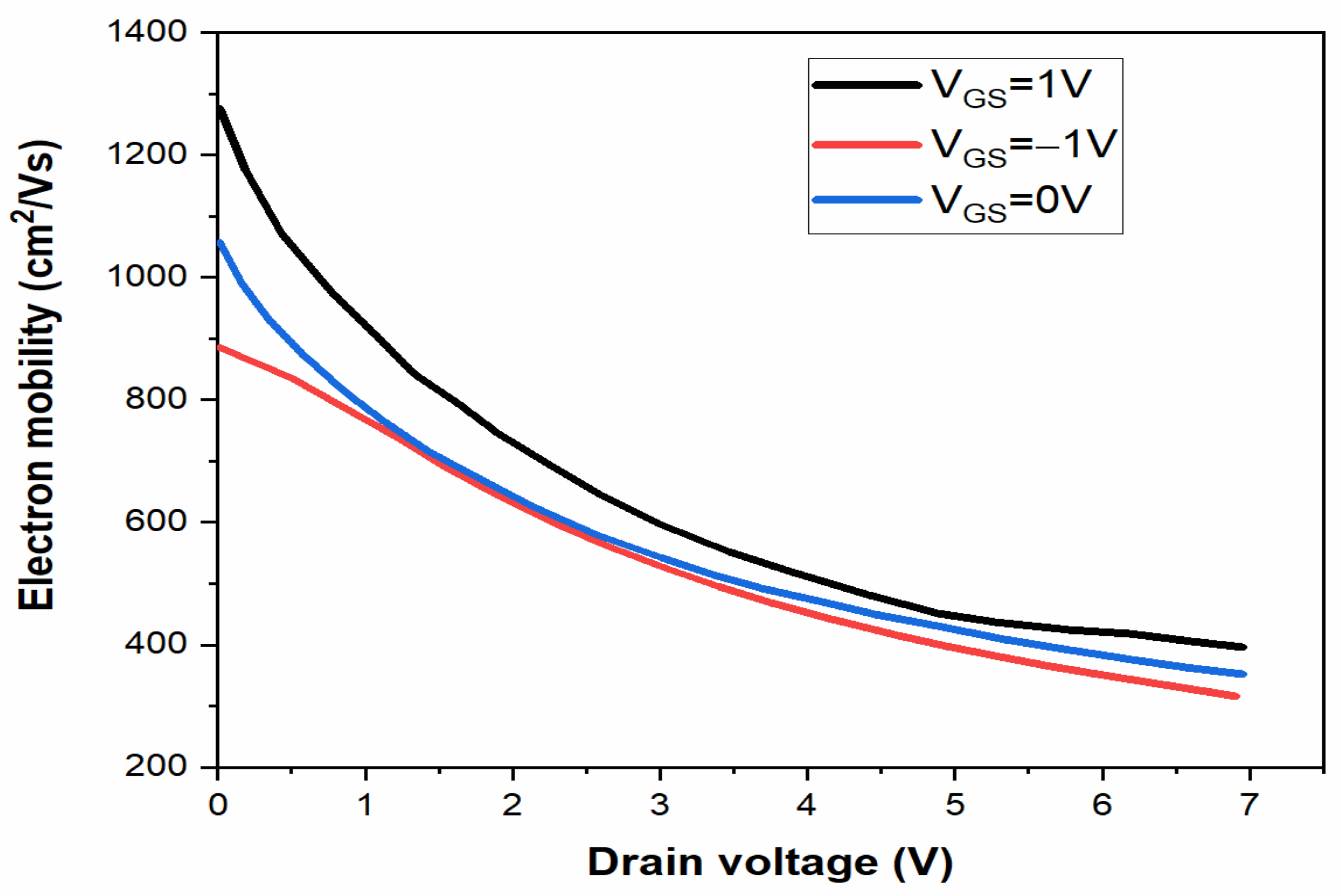
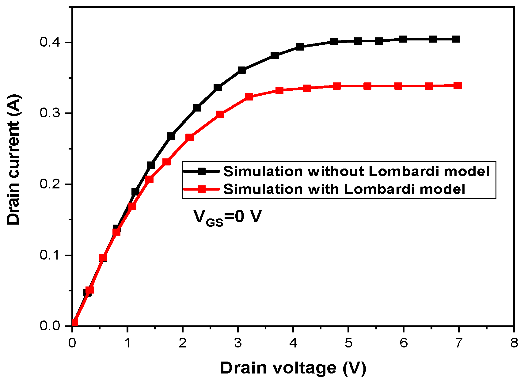
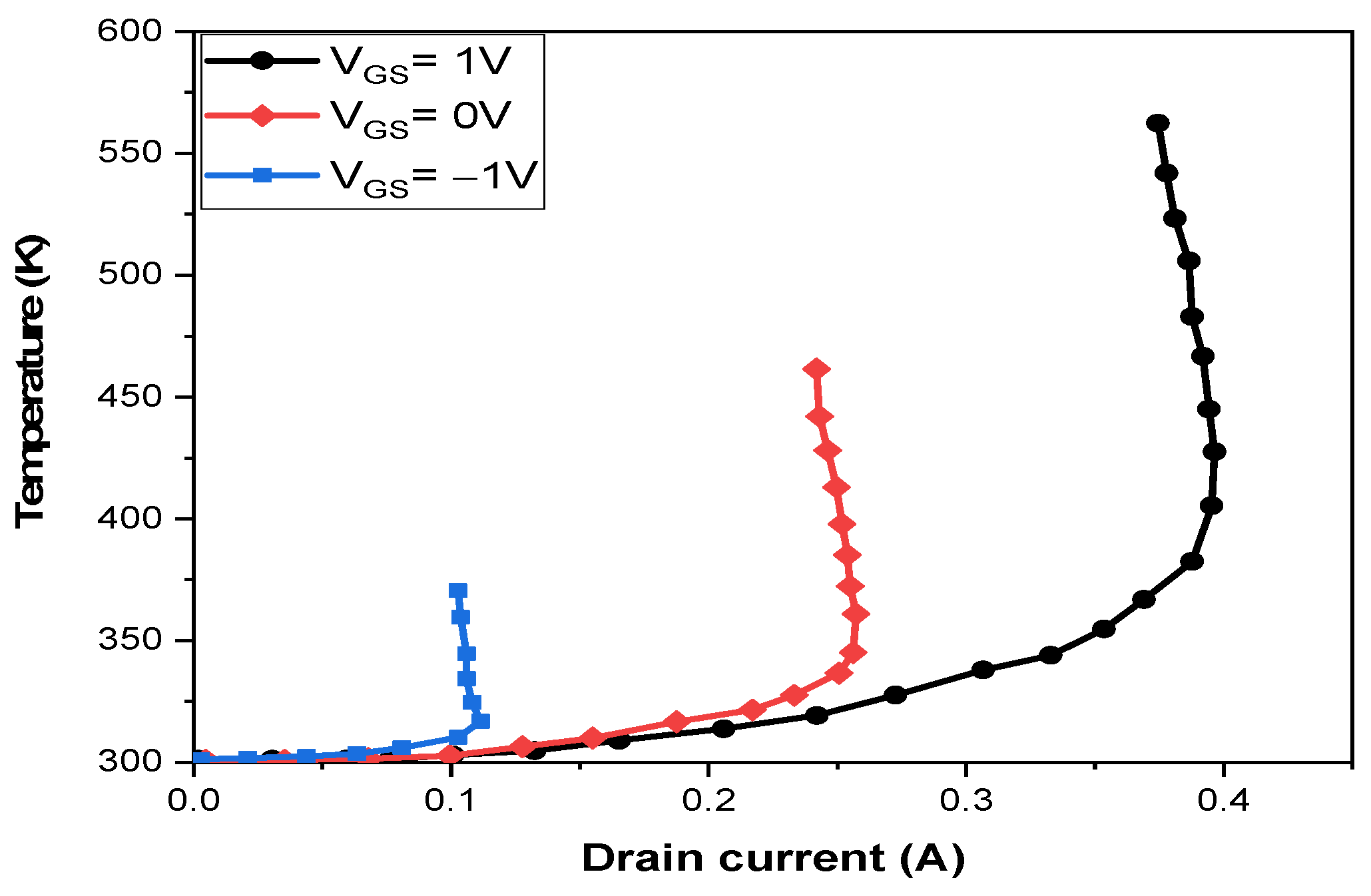
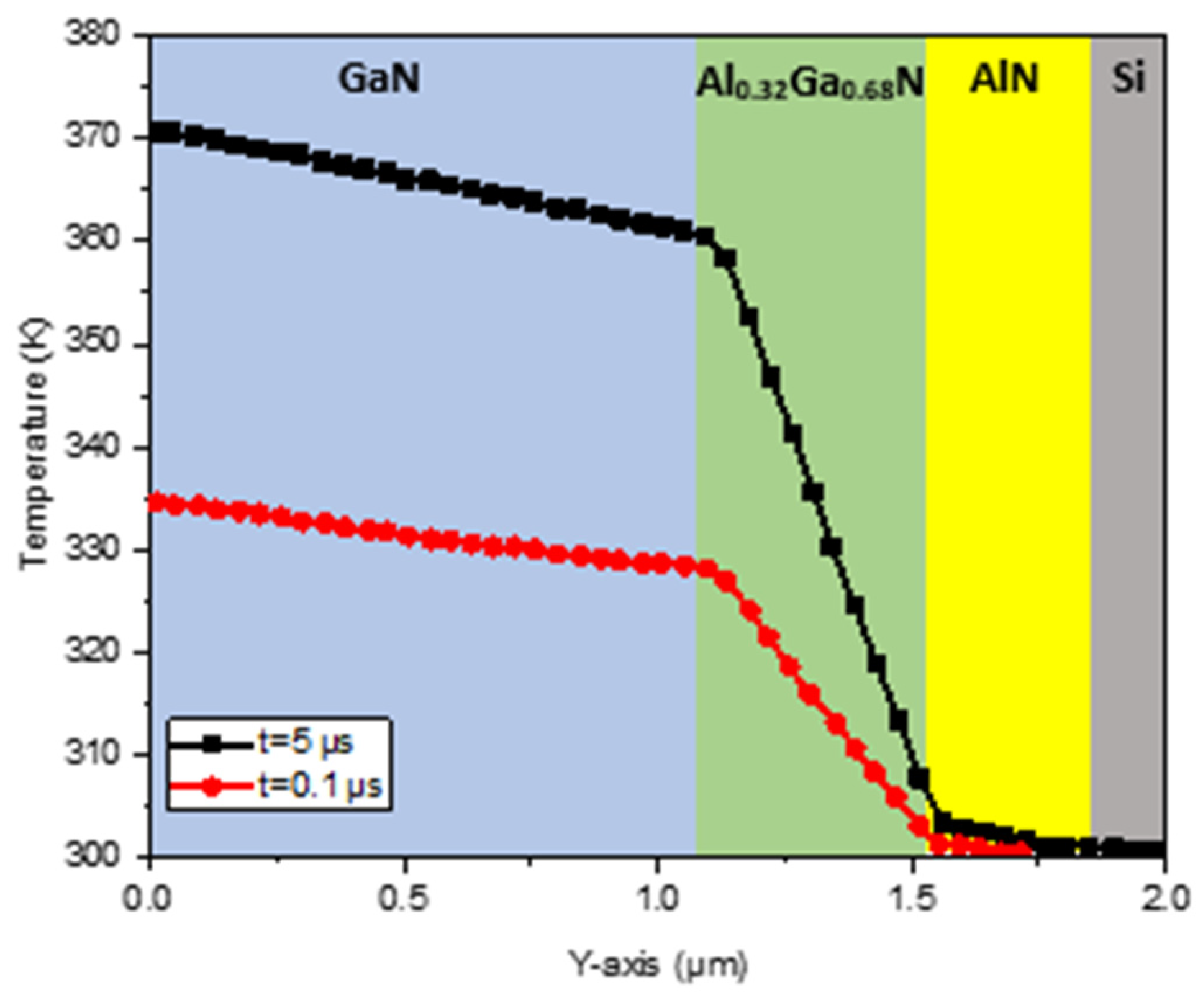
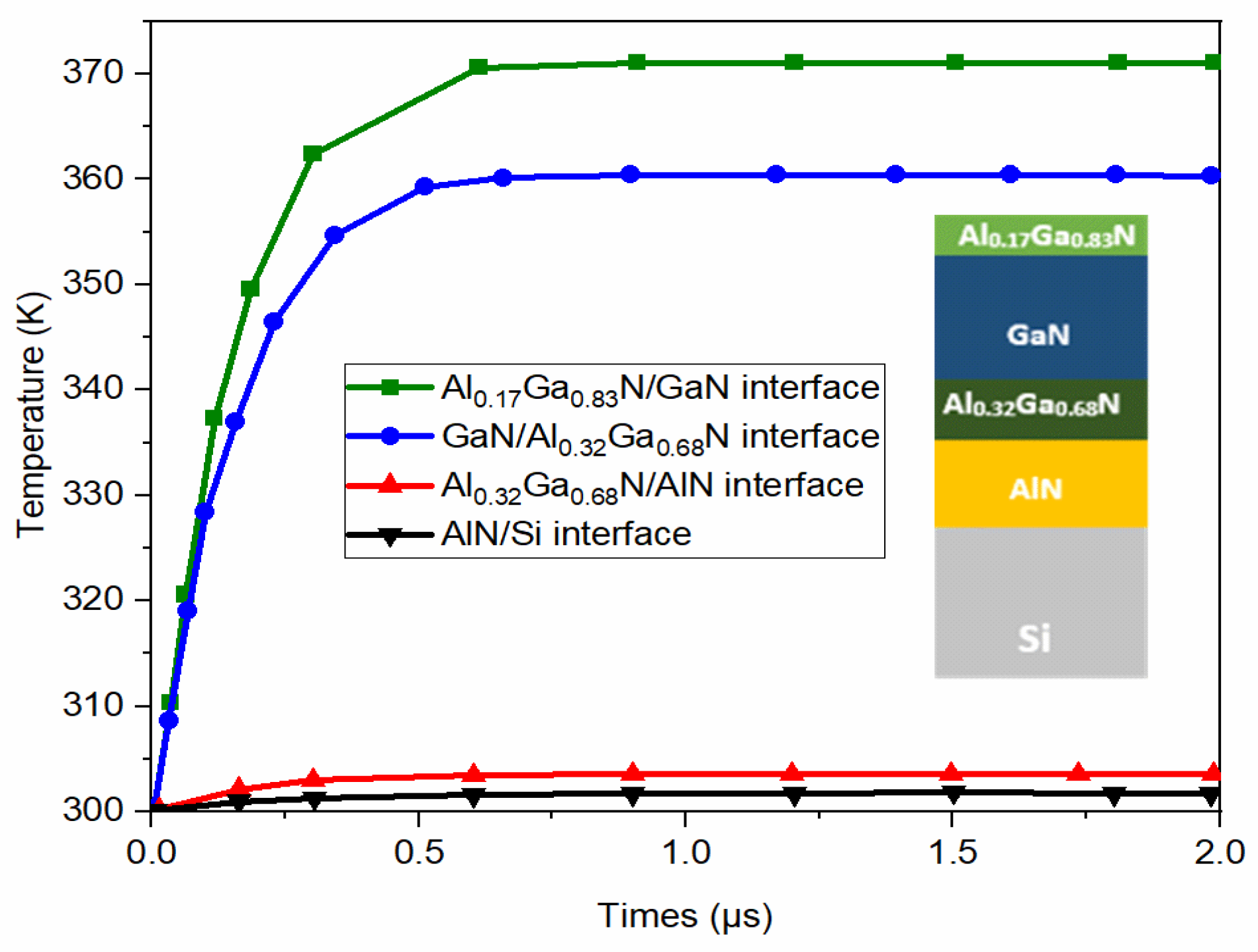
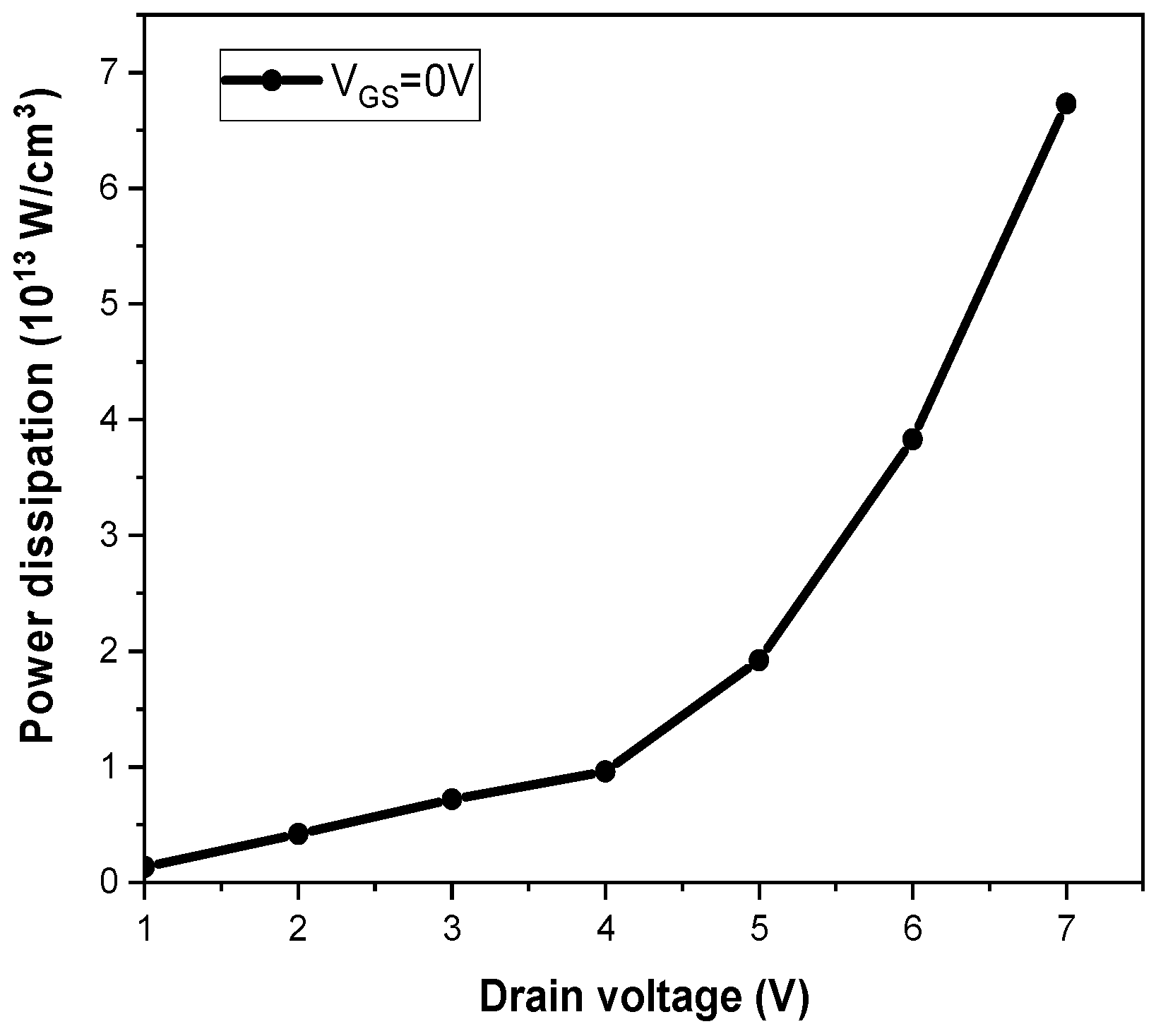
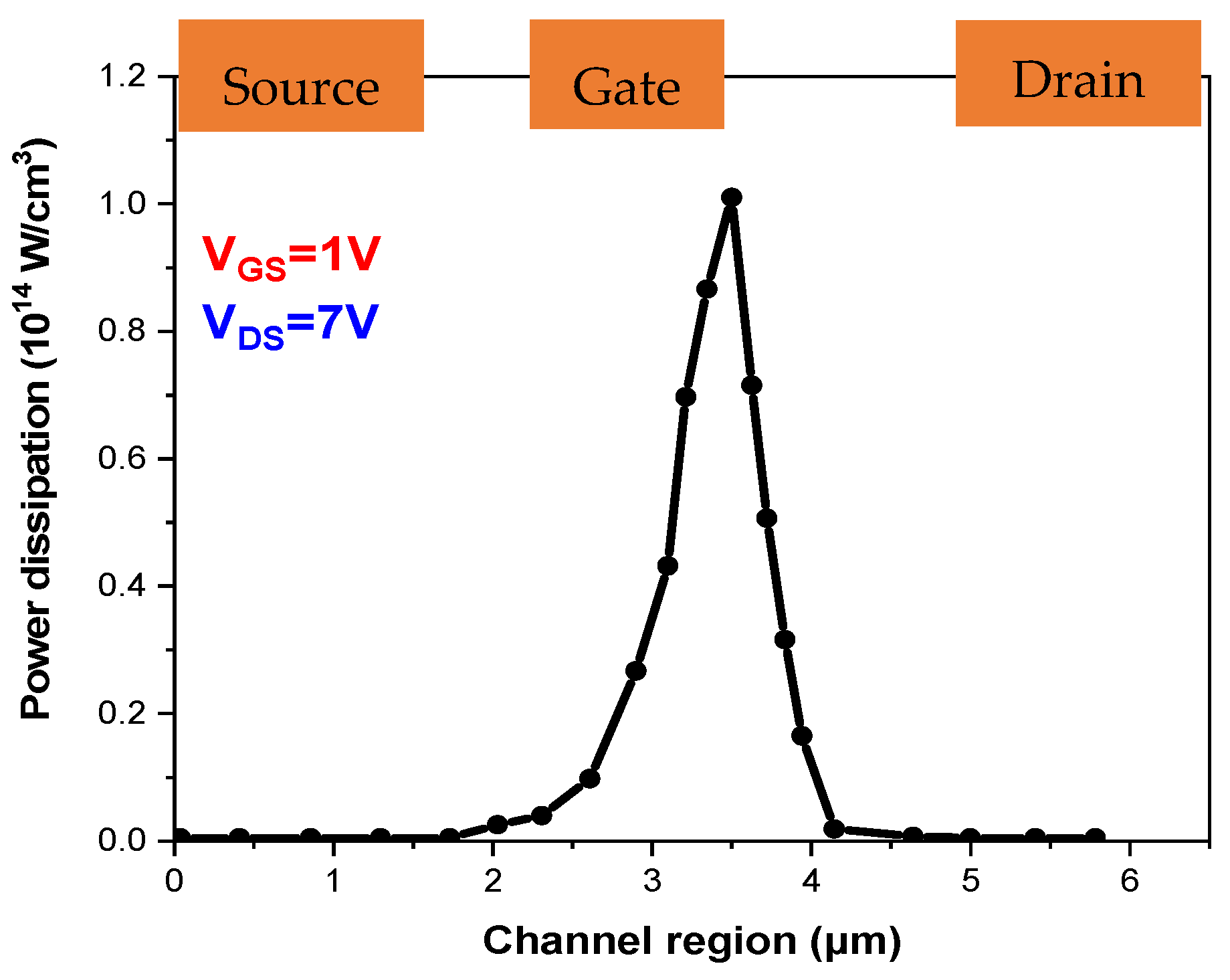
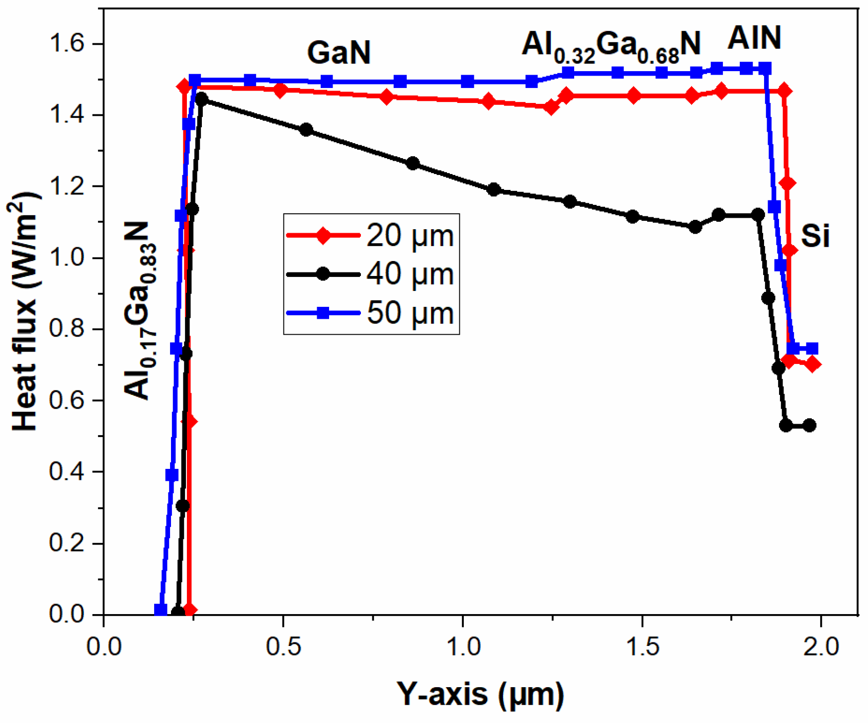
4. Results and Discussion

The primary objective of this work is to investigate the thermal performance of AlGaN/GaN high-electron-mobility transistors (HEMTs) using an electrothermal methodology designed to predict electron conduction and phonon interaction in these electronic devices. The mobility of the two-dimensional electron gas (2DEG) is numerically described, taking into account various contribution factors such as acoustic phonon scattering, polar optical phonon interactions, and interface roughness.
Figure 2 presents a comparison of the temporal temperature profile based on our present simulation using the Callaway phonon relaxation time model, BVK model, and experimental data from [49]. It is obvious that the peak of temperature rise obtained by our proposed model reaches 387 K, the experimental data reach 389 K, and the BVK model reaches 370 K. It is clearly shown that our proposed model captures the same temperature evolution of the studied AlGaN/GaN HEMT as given by experimental works. Consequently, this figure serves as a critical starting point for our research, emphasizing the experimental confirmation of the expanded BDE model using the Callaway phonon relaxation time model.
The evolution of total electron mobility as a function of drain bias at various gate voltage values is depicted in Figure 3. It is evident that an increase in drain voltage corresponds to a decrease in overall carrier mobility. This phenomenon appears in the fact that in high electric fields, the electron velocities reach a maximum, and further increases in VDS do not result in proportional increases in electron mobility. This saturation effect can limit the electron mobility. Moreover, the elevated operating temperature impacts the lattice structure, increases the phonon scattering, and contributes to the electron mobility degradation. Moreover, the electron mobility increases as the gate voltage varies from VGS = −1 V to VGS = 1 V. The positive increase in the gate bias VGS attracts more electrons to the 2DEG channel; there is then an increase of the electron density which potentially leads to improved electron mobility.
Figure 4 depicts the temporal evolution of the effective thermal conductivity, revealing a notable decrease across all layers. This reduction can be attributed to key factors such as material thickness and boundary scattering. In AlxGa1-xN, point defect scattering, mainly caused by impurities and alloy components, is the dominant scattering mechanism due to the presence of Al atoms. In contrast, the impact of these factors on phonon transport is limited in GaN and AlN layers. Notably, among various phonon scattering processes, boundary scattering emerges as the primary mechanism in all layers.
Figure 5 depicts the temperature-dependent thermal conductivity trends of AlGaN, GaN, and AlN layers. Noteworthy is the initial high thermal conductivity of the four materials at ambient temperature, followed by a decline as temperature increases. This drop is a significant challenge for HEMT transistors. This phenomenon is explained by considering phonon behavior: at lower temperature, phonons possess less thermal energy, exhibiting coherent motion within the crystal lattice, thereby contributing to heightened thermal conductivity. However, with increasing temperature, phonons become more energetic and interact with lattice defects, impurities, and grain boundaries. This interaction causes dispersion and a reduction in the phonon mean free path. Moreover, at higher temperatures, Umklapp scattering becomes more intense, further contributing to the observed decrease in thermal conductivity.
Figure 6 depicts the IDS-VDS characteristics, with and without the Lombardi model. When using the Lombardi model, the results show a lower drain current. Alloy disorder scattering and interface roughness scattering are the key factors contributing to lower mobility at the AlGaN/GaN contact. The Lombardi model was used in this investigation to simulate the effect of interface roughness scattering on the properties of AlGaN/GaN HEMTs. As shown in this figure, the contact roughness dispersion causes a significant 20% decrease in saturation current.
Let us now discuss the drain current evolution with operating temperature and Al molar fraction. Therefore, the evolution of the drain current as a function of temperature is shown in Figure 7. It is clearly shown that the rise in drain current in AlGaN/GaN HEMT devices is followed by an increase in device temperature. The device exhibits Joule heating, which occurs when electrical energy is converted into heat due to the intrinsic resistance of the semiconductor materials. Furthermore, the increased drain current causes more power dissipation within the device, which contributes to the temperature rise. As the temperature rises, the thermal resistance increases, increasing the temperature rise. Also, the thermal characteristics of the semiconductor materials utilized in AlGaN/GaN HEMTs are critical. The thermal conductivity of certain materials may decrease at higher temperatures, making it more difficult to effectively transfer heat away from the device.
Figure 8 illustrates the impact of the molar fraction of aluminum, specifically at x = 0.17 and x = 0.32, on the drain current. Notably, the variation in molar fraction plays a significant role in the evolution of the drain current. This is attributed to the increased presence of dislocations resulting from the introduction of aluminum, which occurs due to a mismatch between the crystal structures of AlN and GaN. A higher aluminum content leads to an elevated carrier density; however, the electron mobility attains a peak at a specific aluminum concentration. Beyond this point, the constraints become excessive, resulting in a decrease in mobility due to factors such as interface roughness and dispersion effects. Consequently, this rationale justifies the use of an Al0.32Ga0.68N layer for the bottom transition layer and an Al0.17Ga0.83N layer for the transition layer.
To verify the importance of the contribution and magnitude of interface conductance across the AlGaN–GaN heterostructure, Figure 9 depicts the temperature distribution along the cross-section from the Al0.17Ga0.83N/GaN interface to the bottom of the Si substrate. It is obvious that the highest temperature is observed at the Al0.17Ga0.83N/GaN interface layer, while the temperature discontinuity at the GaN/Al0.32Ga0.68N interface is very significant compared to the Al0.32Ga0.68N/AlN interface. Indeed, a considerable temperature differential arises at the boundary contact because of phonon scattering.
Figure 10 provides the temporal temperature evolution of AlGaN/GaN multilayer structures at different interfaces. We show that there is a rapid increase in temperature that occurs at the GaN/Al0.17Ga0.83N interface. The temperature rise is caused by the power heat generation being distributed evenly over the Al0.17Ga0.83N/GaN interface. However, a decrease in temperature elevation becomes evident as we move away from the HEMT channel region; the temperature elevation decreases, which subsequently explains the lower evolution of temperature at the Al0.32Ga0.68N/AlN and AlN/Si interfaces. Furthermore, it is obvious that the temperature reaches its maximum (370 K) at t = 0.6 μ s and the saturation is well observed.
Figure 11 depicts the Joule heating impact computed by our electrothermal model in an AlGaN/GaN HEMT transistor at VGS = 0 V. Our results show a significant exponential rise in power dissipation with increasing drain voltage, reaching values of 6.83 ×   10 13 W/m3 at VDS = 7 V.
Furthermore, Figure 12 depicts the power dissipation evolution along the x-axis of the HEMT device passed by the channel region at VGS = 1 V and VDS = 7 V. From this figure, we show that the power dissipation is maximum at the end of the channel region on the drain side and decreases rapidly until it vanishes in the drain zone. This peak is caused by the presence of powerful electric field and current density, which causes a localized increase in electric field intensity. Consequently, high-energy hot electrons are generated within this concentrated field zone. These heated electrons move through a highly resistive local depletion zone, creating a limited region where Joule heating occurs.
Figure 13 exhibits the temporal heat flux profiles along the y-axis. At first, the heat flux lines follow each other and reach the maximum. The heat flux has a maximum value of 1.6 ×   10 9 W/m2 at t = 50 μ s at the Al0.17Ga0.83N/GaN interface. It appears as a result of the thermal gradient’s direction, which is determined by the phonon transport dynamics. At t = 20 μ s and at the GaN/Al0.32Ga0.68N interface, the heat flux starts to decrease significantly. This means that the wave propagation of heat flux is dispersed. However, for longer periods, t = 20 μ s and t = 50 μ s , the wave propagation of heat flux disperses to the Al0.32Ga0.68N/AlN interface and subsequently decreases in the AlN/Si interface.

5. Conclusions

In this study, we conducted electrothermal simulations on AlGaN–GaN HEMT transistors. To investigate the electrothermal phenomenon, we employed the enhanced drift-diffusion (D-D) model, which considers total electron mobility factors such as phonon scattering, electron mobility within GaN bulk, and surface roughness. The D-D model was integrated with an enhanced BDE model. Our results reveal that phonon scattering, induced by surface roughness degradation, significantly influences drain current. Moreover, there was a noteworthy increase in power dissipation, reaching 6.8 × 10 13 W/ c m 3 , particularly near the gate’s corner and in proximity to the drain. On the other hand, the Al0.17Ga0.83N/GaN interface played a pivotal role in heat dispersion. Furthermore, we observed a substantial reduction in effective thermal conductivity with rising temperatures, facilitating heat transfer from the channel region to the substrate. This situation emphasizes the crucial role played by the GaN layer in ensuring efficient heat transfer. Additionally, the study detected the prevalence of Umklapp scattering in pure AlN and GaN, along with point-defect scattering in alloys Al0.17Ga0.83N and Al0.32Ga0.68N. It highlights the critical importance of interfaces and size-related effects in reducing thermal conductivity within HEMTs, as well as the significant involvement of phonons in heat transmission within GaN material. This study provides valuable insights for enhancing the thermal performance of HEMT devices.

Author Contributions

Methodology, H.M., F.N., M.A.; Software, H.M. and F.N.; Validation, F.N. and M.M.; Formal analysis, H.M. and M.A.; Data curation, M.A.; Writing—review & editing, F.N.; S.S. and A.G.; Supervision, A.G. All authors have read and agreed to the published version of the manuscript.

Funding

This research was funded by Princess Nourah bint Abdulrahman University Researchers Supporting Project number (PNURSP2023R56), Princess Nourah bint Abdulrahman University, Riyadh, Saudi Arabia.

Data Availability Statement

Data are contained within the article.

Conflicts of Interest

The authors declare no conflict of interest.

References

  1. Pengelly, R.S.; Wood, S.M.; Milligan, J.W.; Sheppard, S.T.; Pribble, W.L. A Review of GaN on SiC High Electron-Mobility Power Transistors and MMICs. IEEE Trans. Microw. Theory Tech. 2012, 60, 1764–1783. [Google Scholar] [CrossRef]
  2. Meneghini, M.; Meneghesso, G.; Zanoni, E. Power GaN Devices; Springer: Cham, Switzerland, 2017. [Google Scholar]
  3. Peralagu, U.; Alian, A.; Putcha, V.; Khaled, A.; Rodriguez, R.; Sibaja-Hernandez, A.; Chang, S.; Simoen, E.; Zhao, S.E.; De Jaeger, B.; et al. CMOS-compatible GaN-based devices on 200 mmSi for RF applications: Integration and performance. In Proceedings of the 2019 IEEE International Electron Devices Meeting (IEDM), San Francisco, CA, USA, 9–11 December 2019; pp. 17.2.1–17.2.4. [Google Scholar]
  4. Karmalkar, S.; Mishra, U.K. Enhancement of breakdown voltage in AlGaN/GaN high electron mobility transistors using a field plate. IEEE Trans. Electron Devices 2001, 48, 1515. [Google Scholar] [CrossRef]
  5. Mishra, U.K.; Parikh, P.; Wu, Y.F. AlGaN/GaN HEMTs overview of device operation and applications. Proc. IEEE 2002, 90, 1022–1031. [Google Scholar] [CrossRef]
  6. Chatterjee, B.; Dundar, C.; Beechem, T.E.; Heller, E.; Kendig, D.; Kim, H.; Choi, S. Nanoscale electro-thermal interactions in AlGaN/GaN high electron mobility transistors. J. Appl. Phys. 2020, 127, 044502. [Google Scholar] [CrossRef]
  7. Ambacher, O.; Smart, J.; Shealy, J.R.; Weimann, N.G.; Chu, K.; Murphy, M.; Schaff, W.J.; Eastman, L.F.; Dimitrov, R.; Wittmer, L. Two-dimensional electron gases induced by spontaneous and piezoelectric polarization charges in N-and Gaface AlGaN/GaN heterostructures. J. Appl. Phys. 1999, 85, 3222–3323. [Google Scholar] [CrossRef]
  8. Siemens, M.E.; Li, Q.; Yang, R.; Nelson, K.A.; Anderson, E.H.; Murnane, M.M.; Kapteyn, H.C. Quasi-ballistic thermal transport from nanoscale interfaces observed using ultrafast coherent soft X-ray beams. Nat. Mater. 2010, 9, 26–30. [Google Scholar] [CrossRef]
  9. McAlister, S.P.; Bardwell, J.A.; Haffouz, S.; Tang, H. Self-heating and the temperature dependence of the dc characteristics of GaN heterostructure field effect transistors. J. Vac. Sci. Technol. A 2006, 24, 624–628. [Google Scholar] [CrossRef]
  10. Meneghesso, G.; Verzellesi, G.; Danesin, F.; Rampazzo, F.; Zanon, F.; Tazzoli, A.; Meneghini, M.; Zanoni, E. Reliability of GaN high-electron-mobility transistors: State of the art and perspectives. IEEE Trans. Device Mater. Reliab. 2008, 8, 332–343. [Google Scholar] [CrossRef]
  11. Luo, X.; Halder, S.; Curtice, W.R.; Hwang, J.C.; Chabak, K.D.; Walker, D.E.; Dabiran, A.M. Scaling and high-frequency performance of AlN/GaN HEMTs. In Proceedings of the 2011 IEEE International Symposium on Radio-Frequency Integration Technology, Piscataway, NJ, USA, 30 November–2 December 2011; pp. 209–212. [Google Scholar] [CrossRef]
  12. Rosker, M.; Bozada, C.; Dietrich, H.; Hung, A.; Via, D.; Binari, S.; Vivierios, E.; Cohen, E.; Hodiak, J. The DARPA wide band gap semiconductors for RF applications (WBGS-RF) program: Phase II results. In Proceedings of the International Conference on Compound Semiconductor Manufacturing Technology, Tampa, FL, USA, 18–21 May 2009. [Google Scholar]
  13. Rezgui, H.; Nasri, F.; Ali, A.B.H.; Guizani, A.A. Analysis of the ultrafast transient heat transport in sub 7-nm SOI FinFETs technology nodes using phonon hydrodynamic equation. IEEE Trans. Electron Devices 2020, 68, 10–16. [Google Scholar] [CrossRef]
  14. Hua, Y.C.; Li, H.L.; Cao, B.Y. Thermal spreading resistance in ballistic-diffusive regime for GaN HEMTs. IEEE Trans. Electron Devices 2019, 66, 3296–3301. [Google Scholar] [CrossRef]
  15. Rezgui, H.; Nasri, F.; Nastasi, G.; Aissa, M.F.B.; Rahmouni, S.; Romano, V.; Belmabrouk, H.; Guizani, A.A. Design optimization of nanoscale electrothermal transport in 10 nm SOI FinFET technology node. J. Phys. D Appl. Phys. 2020, 53, 495103. [Google Scholar] [CrossRef]
  16. Azarifar, M.; Doğacan, K.A.R.A.; Dönmezer, N. Thermal Spreading Performance of Gan-On-Diamond Substrate HEMTs With Localized Joule Heating. J. Therm. Sci. Technol. 2019, 39, 111–119. [Google Scholar]
  17. Donmezer, N.; Islam, M.; Yoder, P.D.; Graham, S. The impact of nongray thermal transport on the temperature of AlGaN/GaN HFETs. IEEE Trans. Electron. Devices 2015, 62, 2437–2444. [Google Scholar] [CrossRef]
  18. Bertoluzza, F.; Delmonte, N.; Menozzi, R. Three-dimensional finite-element thermal simulation of GaN-based HEMTs. Microelectron. Reliab. 2009, 49, 468–473. [Google Scholar] [CrossRef]
  19. Bao, H.; Chen, J.; Gu, X.; Cao, B.-Y. A review of simulation methods in micro/nanoscale heat conduction. ES Energy Environ. 2018, 1, 16–55. [Google Scholar] [CrossRef]
  20. Guo, Z.-Y. Energy-mass duality of heat and its applications. ES Energy Environ. 2018, 1, 4–15. [Google Scholar] [CrossRef]
  21. Hua, Y.-C.; Cao, B.-Y. Ballistic-diffusive heat conduction in multiply-constrained nanostructures. Int. J. Therm. Sci. 2016, 101, 126–132. [Google Scholar] [CrossRef]
  22. Yalamarthy, A.S.; So, H.; Muñoz Rojo, M.; Suria, A.J.; Xu, X.; Pop, E.; Senesky, D.G. Tuning electrical and thermal transport in AlGaN/GaN heterostructures via buffer layer engineering. Adv. Funct. Mater. 2018, 28, 1705823. [Google Scholar] [CrossRef]
  23. Hao, Q.; Zhao, H.; Xiao, Y.; Kronenfeld, M.B. Electrothermal studies of GaN-based high electron mobility transistors with improved thermal designs. Int. J. Heat Mass Transf. 2018, 116, 496–506. [Google Scholar] [CrossRef]
  24. Freedman, J.P.; Leach, J.H.; Preble, E.A.; Sitar, Z.; Davis, R.F.; Malen, J.A. Universal phonon mean free path spectra in crystalline semiconductors at high temperature. Sci. Rep. 2013, 3, 2963. [Google Scholar] [CrossRef]
  25. Park, K.; Bayram, C. Impact of dislocations on the thermal conductivity of gallium nitride studied by time-domain thermoreflectance. J. Appl. Phys. 2019, 126, 185103. [Google Scholar] [CrossRef]
  26. Liu, W.; Balandin, A.A. Thermal conduction in AlxGa1-xN alloys and thin films. J. Appl. Phys. 2005, 97, 073710. [Google Scholar] [CrossRef]
  27. Lisesivdin, S.B.; Yildiz, A.; Et Kasap, M. Optimization of alloy composition, interlayer and barrier thicknesses in AlxGa1-xN/(AlN)/GaN high electron mobility transistors. Strain 2007, 10, 35. [Google Scholar]
  28. Gurusinghe, M.N.; Davidsson, S.K.; Andersson, T.G. Two-dimensional electron mobility limitation mechanisms in AlxGa1-xN/GaN heterostructures. Phys. Rev. B 2005, 72, 045316. [Google Scholar] [CrossRef]
  29. Liu, B.; Lu, Y.W.; Jin, G.R.; Zhao, Y.; Wang, X.L.; Zhu, Q.S.; Wang, Z.G. Surface roughness scattering in two dimensional electron gas channel. Appl. Phys. Lett. 2010, 97, 262111. [Google Scholar] [CrossRef]
  30. Zhang, J.; Hao, Y.; Zhang, J.; Ni, J. The mobility of two-dimensional electron gas in AlGaN/GaN heterostructures with varied Al content. Sci. China Ser. F Inf. Sci. 2008, 51, 780–789. [Google Scholar] [CrossRef]
  31. Chen, G. Ballistic-diffusive heat conduction equations. Phys. Rev Lett. 2001, 86, 2297. [Google Scholar] [CrossRef]
  32. Chen, G. Ballistic-diffusive equations for transient heat conduction from nano to macroscales. J. Heat Transfer. 2002, 124, 320–328. [Google Scholar] [CrossRef]
  33. Rezgui, H.; Nasri, F.; Aissa, M.F.B.; Belmabrouk, H.; Guizani, A.A. Modeling the thermal performance of nano-GNRFET transistors using ballistic-diffusive equation. IEEE Trans. Electron Devices 2018, 65, 1611–1616. [Google Scholar] [CrossRef]
  34. Mitterhuber, L.; Hammer, R.; Dengg, T.; Spitaler, J. Thermal characterization and modelling of AlGaN-GaN multilayer structures for HEMT applications. Energies 2020, 13, 2363. [Google Scholar] [CrossRef]
  35. Romano, V.; Rusakov, A. 2d numerical simulations of an electron–phonon hydrodynamical model based on the maximum entropy principle. Comput. Methods Appl. Mech. Eng. 2010, 199, 2741–2751. [Google Scholar] [CrossRef]
  36. Lombardi, C.; Manzini, S.; Saporito, A.; Vanzi, M. A physically based mobility model for numerical simulation of nonplanar devices. IEEE Trans. Comput.-Aided Des. Integr. Circuits Syst. 1988, 7, 1164–1171. [Google Scholar] [CrossRef]
  37. Du, J.; Yan, H.; Yin, C.; Feng, Z.; Dun, S.; Yu, Q. Simulation and characterization of millimeter-wave InAlN/GaN high electron mobility transistors using Lombardi mobility model. J. Appl. Phys. 2014, 115, 164510. [Google Scholar] [CrossRef]
  38. Device Simulation Software. In ATLAS User’s Manual; SILVACO International: Santa Clara, CA, USA, 1998; Volume II, pp. 567–1000.
  39. Tzou, D.Y. Macro- to Microscale Heat Transfer: The Lagging Behavior; Taylor & Francis: Washington, DC, USA, 1997. [Google Scholar]
  40. Ordonez-Miranda, J.; Yang, R.; Alvarado-Gil, J.J. A constitutive equation for nano-to-macro-scale heat conduction based on the Boltzmann transport equation. J. Appl. Phys. 2011, 109, 084319. [Google Scholar] [CrossRef]
  41. Minnich, A.J.; Chen, G.; Mansoor, S.; Yilbas, B.S. Quasiballistic heat transfer studied using the frequency-dependent Boltzmann transport equation. Phys. Rev. B 2011, 84, 235207. [Google Scholar] [CrossRef]
  42. Chen, G. Non-Fourier phonon heat conduction at the microscale and nanoscale. Nat. Rev. Phys. 2021, 3, 555–569. [Google Scholar] [CrossRef]
  43. Dong, Y.; Cao, B.Y.; Guo, Z.Y. Ballistic–diffusive phonon transport and size induced anisotropy of thermal conductivity of silicon nanofilms. Phys. E Low-Dimens. Syst. Nanostructures 2015, 66, 1–6. [Google Scholar] [CrossRef]
  44. Rezgui, H.; Nasri, F.; Aissa, M.F.B.; Blaabjerg, F.; Belmabrouk, H.; Guizani, A.A. Investigation of heat transport across Ge/Si interface using an enhanced ballistic-diffusive model. Superlattices Microstruct. 2018, 124, 218–230. [Google Scholar] [CrossRef]
  45. Lucchesi, C.; Vaillon, R.; Chapuis, P.O. Temperature dependence of near-field radiative heat transfer above room temperature. Mater. Today Phys. 2021, 21, 100562. [Google Scholar] [CrossRef]
  46. Klemens, P.G.; White, G.K.; Tainsh, R.J. Scattering of lattice waves by point defects. Philos. Mag. 1962, 7, 1323–1335. [Google Scholar] [CrossRef]
  47. Wang, Z.; Alaniz, J.E.; Jang, W.; Garay, J.E.; Dames, C. Thermal conductivity of nanocrystalline silicon: Importance of grain size and frequency-dependent mean free paths. Nano Lett. 2011, 11, 2206–2213. [Google Scholar] [CrossRef] [PubMed]
  48. Jang, K.W.; Hwang, I.T.; Kim, H.J.; Lee, S.H.; Lim, J.W.; Kim, H.S. Thermal analysis and operational characteristics of an AlGaN/GaN High electron mobility transistor with copper-filled structures: A simulation study. Micromachines 2019, 11, 53. [Google Scholar] [CrossRef] [PubMed]
  49. Peierls, R. Zur kinetischen Theorie der Wärmeleitung in Kristallen. Ann. Phys. 1929, 395, 1055–1101. [Google Scholar] [CrossRef]
Figure 1. Schematic geometry of AlGaN–GaN HEMT.
Electronics 13 00164 g001
Figure 2. Comparison of the temporal temperature profile.
Electronics 13 00164 g002
Figure 3. Total electron mobility evolution versus drain voltage at different values of VGS.
Electronics 13 00164 g003
Figure 4. Temporal evolution of effective thermal conductivity: (a) GaN and AlN, (b) Al0.17Ga0.83N and Al0.32Ga0.68N.
Electronics 13 00164 g004
Figure 5. Evolution of thermal conductivities with temperature: (a) GaN and AlN, (b) Al0.17Ga0.83N and Al0.32Ga0.68N at t = 5 µs.
Electronics 13 00164 g005
Figure 6. Evolution of DC characteristics with and without Lombardi model.
Electronics 13 00164 g006
Figure 7. Evolution of temperature versus drain current at different values of drain–source voltage.
Electronics 13 00164 g007
Figure 8. Variation of drain current with drain–source voltage for various Al mole fraction x at VGS = 0 V.
Electronics 13 00164 g008
Figure 9. Temperature evolution along the y-direction with y = 0 at the Al0.17Ga0.83N interface.
Electronics 13 00164 g009
Figure 10. Temperature evolution analysis at AlGaN–GaN heterostructure interfaces.
Electronics 13 00164 g010
Figure 11. Evolution of power dissipation versus drain voltage at VGS = 0 V.
Electronics 13 00164 g011
Figure 12. Evolution of the power dissipation versus channel region at VGS = 1 V and VDS = 7 V.
Electronics 13 00164 g012
Figure 13. Heat flux profiles in the y-axis for GaN, Al0.17Ga0.83N, Al0.32Ga0.64N, AlN, and Si at different times.
Electronics 13 00164 g013
Table 1. Thermal characteristics of materials [34].
S y m b o l V S ( m . s 1 ) k 300 ( W . m 1 . K 1 ) C ( J m 3 K 1 )
Si30001501.5 ×   10 6
AlN7228.241302.67 ×   10 6
GaN4997.52202.63 ×   10 6
Al0.32Ga0.68N5899.069.72.65 ×   10 6
Al0.17Ga0.83N5899.0611.42.65 ×   10 6
Table 2. GaN low-field mobility model parameters.
μ 300 μ m i n 300 α α 1 α 2
1250   c m 2 / V s 100   c m 2 / V s 0.065−1.5−0.2
Table 3. Fitted values of the α parameter using an experimental value of thermal conductivities for four materials.
Materials α Parameter
GaN−1.84 ± 0.05
AlN−1.8 ± 0.07
Al0.17Ga0.68N−0.27 ± 0.007
Al0.32Ga0.68N−0.25 ± 0.007
Table 4. Parameters of phonon scattering for three models [34].
MaterialsCallaway ModelBVK Model
β Γ G β Γ G
AlN3 3   × 10−40.43.810−50.3
GaN3 2   × 10−410.8 9   × 10−51
Al0.32Ga0.67N30.056130.41
Al0.17Ga0.83N30.030.8530.20.96
Disclaimer/Publisher’s Note: The statements, opinions and data contained in all publications are solely those of the individual author(s) and contributor(s) and not of MDPI and/or the editor(s). MDPI and/or the editor(s) disclaim responsibility for any injury to people or property resulting from any ideas, methods, instructions or products referred to in the content.

