
Full-Custom 90 nm CNTFET Process Design Kit: Characterization, Modeling, and Implementation
by
Liming Chen
1, 
Yuyan Zhang
2,
Zhifeng Chen
3,
Jiming Chen
3,
Huangwei Chen
3,
Jianhua Jiang
2,* and
Chengying Chen
3,* 1
School of Integrated Circuits, Beijing University of Posts and Telecommunications, Beijing 100876, China
2
School of Electronics, Peking University, Beijing 100871, China
3
School of Opto-Electronic and Communication Engineering, Xiamen University of Technology, Xiamen 361024, China
*
Authors to whom correspondence should be addressed.
Electronics 2024, 13(3), 605; https://doi.org/10.3390/electronics13030605
Submission received: 12 January 2024
/
Revised: 29 January 2024
/
Accepted: 31 January 2024
/
Published: 1 February 2024
(This article belongs to the Special Issue High Carrier Mobility Devices Technology and Applications)
Abstract
:As the semiconductor industry enters the post-Moore era, the carbon nanotube field-effect transistor (CNTFET) has become a powerful substitute for silicon-based transistors beyond 5 nm process nodes due to its high mobility, low power consumption, and ultra-thin-body electrical advantages. Carbon-based transistor technology has made significant progress in device manufacture and preparation, but carbon-based process design kits (PDKs) that meet the standards of commercial design tools are still an important bottleneck hindering the development of carbon-based integrated circuits. For the first time, a complete full-custom 90 nm CNTFET PDK is proposed in this paper, which includes Pcells for transistors, resistors, and capacitors; a compact model; DRC/LVS/PEX rules; and a standard cell and timing library. It can support the entire design flow of analog, digital, and mixed-signal carbon-based integrated circuits. To achieve an accurate compact model, the back-gate effect of CNTFETs and the influence of gate/drain voltage on transport probability are analyzed. Then the theoretical formulas for mobility and channel current are established. The comparison of the simulation and test results of CNTFET characteristics proves the accuracy of the compact model. Using this PDK, combined with standard IC design tools and design flow, the circuit and layout of an operational amplifier, SRAM, and 8-bit counter are completed. The simulation results verify the correctness and effectiveness of the PDK, laying a solid foundation for the large-scale industrialization of carbon-based integrated circuits.
1. Introduction
After more than half a century of development, silicon-based integrated circuits are now scaling to the nanoscale. The emergence of three-dimensional transistor structures at the 22 nm process node allowed for the continuation of Moore’s law. However, entering the post-Moore era, narrow channel effects such as carrier saturation, mobility reduction, and source/drain tunneling at 5 nm or even smaller process nodes pose serious challenges to the development of silicon-based transistors. The International Technology Roadmap for Semiconductors (ITRS) made carbon nanotubes an important choice for future integrated circuit materials as early as 2009 [1,2,3,4]. Carbon nanotubes can be divided into two categories: single-walled and multi-walled. Multi-walled carbon nanotubes can be regarded as nested single-walled carbon nanotubes. Due to their fewer defects, simple structure, good controllability, and high semiconductor ratio compared to multi-walled carbon nanotubes, carbon-based integrated circuit technology is mainly developed by single-walled carbon nanotubes [5,6,7,8,9].
The CNTFET has a quasi-one-dimensional structure, and the movement of electrons in nanotubes is strictly restricted. Electrons can only move freely along the axis of the tube and will not undergo wide-angle scattering. Therefore, the gate voltage can effectively control the on/off of transistors and reduce the leakage current. Meanwhile, due to its extremely long mean free path (MFP) (~1 μm), carriers can achieve quasi-ballistic transport in a channel and have extremely high mobility. The CNTFET not only provides significant current transfer capability in low-voltage environments but also has extremely high characteristic frequencies (fT). Hundreds of nanowires can be prepared as conductive channels in the same CNTFET, further increasing its current density [10,11,12,13,14,15,16]. These advantages provide solutions for the implementation of nanoscale carbon-based VLSI analog/logic circuits.
In recent years, the CNTFET has made significant progress in materials, devices, and small-scale logic circuits. The achievements of integrated circuits such as carbon-based logic gates, ring oscillators, and amplifiers, even microprocessors, are constantly emerging. However, as a bridge between circuit design and process integration, the PDK remains an important missing link in the research field of CNTFET integrated circuits. As a necessary condition for large-scale integrated circuit simulation and verification, a carbon-based PDK that meets commercial simulation tools has become a technical bottleneck that urgently needs to be broken through. A complete PDK must include Pcells, compact models, DRC/LVS/PEX rules, and a standard cell and timing library for carbon-based transistors, resistors, and capacitors. It can also support the analog, digital, and mixed-signal carbon-based integrated circuit design flows of industry simulation tools such as Cadence Virtuoso/Synopsys HSPICE/SIEMENS EDA Calibre. As of now, only Chenlin Shi et al. have established a standard cell library for 7 nm CNTFETs based on the open-source VS-CNTFET [17]. This standard cell library consists of 56 logic gates. With this standard cell library, they designed a 64-bit full adder circuit and layout and compared it with the design results of the ASAP7 model. There is still a significant gap between this carbon-based standard cell library and the complete PDK. Firstly, it does not extract parameters according to real carbon-based devices, and the compact model cannot truly reflect their performance, making it only of academic research value. Secondly, due to the lack of rule files such as DRC/LVS/PEX and a digital timing library, designers are unable to use this standard cell library for conventional carbon-based analog/digital integrated circuit design and verification.
As the core part of an integrated circuit simulation, compact models are also the most important component of carbon-based PDKs. However, current research on CNTFET compact models is only concentrated in a few research institutions. Some achievements have explored their intrinsic current, port capacitor, and transport characteristics, but a mature and compact model that conforms to the design flow of commercial simulation tools has not yet been formed. Ref. [18] first proposed a complete SPICE compact model for a 32 nm CNTFET process node. This model was implemented using Verilog-A, supports HSPICE, and includes quantum effects, acoustic/optical phonon scattering effects, and shielding effects between multiple nanowires. Ref. [19] expanded the research on the basis of ref. [18], adding a channel elastic scattering effect, a drain/source series resistor, a Schottky barrier resistor, and a parasitic gate capacitor to the intrinsic small-signal compact model. These non-ideal factors make the model closer to the actual experimental results. However, the above two research results adopted a simplified energy band structure, which limits their use in applications that require high power supply and high surface potential. Meanwhile, the diffusion capacitor generated by the minority carriers at the source/drain junction was ignored. Although this is a high-order effect, the diffusion capacitor may affect the AC response of high-frequency small-signal analog circuits. The compact model in refs. [20,21] focuses on the intrinsic characteristics of CNTFETs, combining numerical analysis and semi-empirical methods to model the Schottky barrier and the ballistic transport mechanism. Without analyzing the parasitic capacitor and the tunneling current in the channel, it greatly reduces its usability and authenticity. Ref. [22] proposes a semi-analytical compact model based on a virtual source (VS) model for 9 nm process node applications. This model includes a series resistor, a parasitic capacitor, and direct source/drain tunneling leakage. The model was calibrated with corresponding experimental data, and the results showed that the contact resistor is a key limiting factor for CNTFET performance. Refs. [23,24] proposed a data calibration VS compact model with intrinsic current-voltage and charge-voltage characteristics. This is a relatively complete compact model research achievement to date. So far, all the reported models have assumed that CNTFETs have ideal ballistic transport channels and that carrier transport is mainly controlled by the front-gate. In practice, however, the CNTFET is a dual-gate structure. Compared with the predicted intrinsic properties through theoretical research, there is a modulation effect of the back-gate on the conductive channel. On one hand, engineers can construct n-type and/or p-type CNTFETs based on different back-gate bias voltages. On the other hand, the back-gate of the dual-gate CNTFET provides an additional degree of freedom to regulate the conductive channel, thereby affecting the current, the threshold voltage, and so on. This paper proposes a compact model of a dual-gate CNTFET that includes back-gate effects. The principle of the back-gate effect is analyzed, and the relationship between back-gate voltage and threshold voltage is derived. In addition, the impact of gate voltage and drain voltage on transport probability is also discussed, which improves the calculation accuracy of the channel current. Comparing the simulation results with the test results, the two have good consistency. The previous achievement can only support a digital integrated circuit design flow. The proposed PDK in this paper includes a resistor/capacitor model and supports industry analog/digital simulation tools. It also improved the dual-gate compact model. Therefore, our work is the first completed PDK for CNTFETs.
This paper is organized as follows: Section 2 briefly reviews the CNTFET process. Section 3 describes the PDK, including the proposed transistor model, the layout design rules, and the verification of the proposed model. A standard cell library into an entire backend design flow is also presented. Section 4 discuss the IC implementation of our PDK. Finally, conclusions are drawn in Section 5.
2. Review of the CNTFET Process
At present, CNTFETs are mainly prepared with two methods: Chemical Vapor Deposition (CVD) and solution-based purification and self-assembly. The most obvious advantage of CVD is that it can directly realize parallel-arranged, clean-surface, and fewer defect carbon nanotube arrays on substrates, which has been widely adopted. However, most of these arrays only have a certain parameter of high-density, high-purity, or directional arrangement, which is far from meeting the comprehensive requirements of integrated circuit applications [25,26,27,28]. The solution-based purification and self-assembly technology is a more effective method for preparing CNTFETs. The core idea of this technology is as follows: firstly, the original carbon nanotubes grown by arc discharge or CVD methods are subjected to multiple solution dispersion and separation purification to obtain ultra-high-purity or even chiral-enriched semiconductor carbon nanotube solutions. Then, the self-assembly is carried out to arrange them on the target substrate, ultimately obtaining ultra-high-purity and high-density parallel arrays of carbon nanotubes. Therefore, the CNTFET process in this paper was prepared with this solution-purification and self-assembly technology.
Based on the proposed dimensional-constrained method for carbon nanotube self-assembly technology, purified semiconductor carbon nanotubes are attracted from the bulk solution to the dual liquid phase interface (i.e., carbon nanotubes are transferred from three-dimensional space to the two-dimensional plane) [29]. Afterward, the carbon nanotubes at the dual liquid phase interface are slowly transferred to the solid–liquid gas boundary by wafer pulling and the evaporation convection of the top solvent and are continuously deposited on the wafer surface (i.e., the carbon nanotubes transfer from the two-dimensional plane to the one-dimensional intersection of the wafer and the liquid phase surface). By optimizing process parameters such as the liquid phase interface properties, the wafer pulling and solvent evaporation rate, the carbon nanotube concentration in suspension, and the interaction strength between conjugated polymers and the surface of the carbon nanotubes, this method can prepare 100–200 nanotubes/μm with controllable density, an orientation angle deviation less than 8.3°, and a diameter of 1.45 ± 0.23 nm. Solution-based dispersion and purification technology is another core optimization technology adopted. This method uses polycarbazole conjugated polymers as dispersants; adopts multiple ultrasonic dispersion, high-speed centrifugation separation, and filtration screening; and ultimately yields a semiconductor carbon nanotube solution with a purity of at least 99.9995%. By combining dimensional-constrained self-assembly and highly optimized solution-based dispersion purification technologies, the prepared wafer-level carbon nanotube parallel array can basically meet the needs of practicality and the industrialization of carbon-based integrated circuits. The CNTFET manufactured can achieve a saturation current of 1.3 mA/μm at an operation voltage of 1 V with a peak transconductance of 0.9 mS/μm and a subthreshold slope (SS) of 75 mV/dec. The prepared dual-gate CNTFET structure and the SEM microphotograph are shown in Figure 1, with a heavily doped substrate as the back-gate.
When Lg = 200 nm, the current-voltage characteristics of the P-CNTFET are shown in Figure 2.
3. Compact Model, PDK, and Standard Cell Library
3.1. Compact Model
and are used to represent the threshold voltage and back-gate voltage of the CNTFET, respectively. Based on the derivation of our previous research, it can be concluded that [30]
and represent the difference in work functions between the front-gate, the back-gate, and the substrate, respectively. is the voltage drop on the oxide layer at the back-gate, is the fixed charge in the gate oxide layer, and and are the gate oxide layer capacitors per unit area of the back-gate and front-gate, respectively. From the equation, it can be seen that the threshold voltage of the CNTFET is directly affected by the back-gate voltage and the work function. When the drain voltage Vds is small (Vds < 0.1 V) and its modulation effect on the conductive channel can be ignored, it can be considered that when the channel current is greater than 100 nA, the CNTFET conducts. Meanwhile, the surface potential increases with the increase in the back-gate voltage, while the threshold voltage decreases with the increase in it. Increasing will result in a decrease in the required external voltage to reach a fixed current value and a further decrease in the threshold voltage. Therefore, the back-gate can have an impact on the channel current from both direct and indirect aspects. These two effects need to be accurately characterized in a compact model.
In a channel, due to the quasi-one-dimensional characteristics, most scattering mechanisms are suppressed, so phonon scattering is the most important scattering mechanism. In this case, the direct impact of phonon scattering is to reduce the transport probability, which will lead to a decrease in current. In CNTFETs, the injection of carriers depends on the transport probability and the drain/source voltage. For one-dimensional systems, the Landauer–Buttiker approximation can be used to calculate the current flowing from the drain to the source [31]:
T(E) is the coefficient related to energy transfer, is the Fermi–Dirac distribution, E is the energy, and and are the Fermi energy of source and drain, respectively. Due to the ballistic transport characteristics of the CNTFET, as long as the carrier energy is higher than the top of the channel barrier, it can be directly transported to the drain. So T(E) is approximately 1, and its conductivity is controlled by the drain and gate voltage. However, when the carrier transport is not completely ballistic, its transport probability is also affected by the scattering mechanism. At this point, the T(E) value decreases. As the gate voltage increases, the surface potential increases and the energy band in the channel region decreases. The number of empty sub-states that can undergo electronic transitions decreases. Meanwhile, the scattering MPF increases and the transport probability of the carrier increases. The drain voltage can also have an impact on scattering. As the drain voltage increases, the transport probability and the Fermi distribution function of electrons from drain to source decrease and the total current increases. Therefore, the drain voltage can also have an impact on scattering by affecting the Fermi distribution function.
In order to accurately characterize the compact model, it is necessary to associate the Fermi distribution function of the CNTFET source and drain, as well as the transport probability of the source and drain carriers with the gate voltage. Therefore, it can be obtained that [32]
The three coefficients coeffvg0, coeffvg1, and coeffvg2 represent the relationship between mobility, the Fermi distribution function, and the gate voltage, thereby indirectly reflecting the transport probability of the current. The key expression is as follows:
coeffvg0, coeffvg1, and coeffvg2 can correct the ids-vgs-vds characteristic curve in the compact model. As shown in Figure 3, the comparison between simulation and testing results shows a good agreement.
Then a complete compact model can be built using Verilog-A. The main model parameters are shown in Table 1.
3.2. Full-Custom PDK
The design flow of the CNTFET PDK is shown in Figure 4. At the beginning, it is necessary to first define the basic process parameters (oxide layer thickness, mobility, etc.), device type (transistor, resistor, capacitor), layer information, and supported EDA tools (Cadence Virtuoso/innovus, Synopsys HSPICE/IC compiler, and SIEMENS EDA Calibre) [33].
The devices in the 90 nm CNTFET PDK include L-type and E-type CNTFETs, carbon-based/metal resistors, capacitors, and diodes. The L/E-type P-CNTFET and layer information are shown in Figure 5. The layer description is shown in Table 2.
To support various simulation tools and corresponding processes, the views of devices include symbol, spectrum, hspiceD, auLvs, auCdl, ivpcell, and layout (Pcell). In order to achieve the expected performance and meet manufacturability, the DRC rules must be strictly specified. Taking the L-type P-CNTFET as an example, the DRC rule definition and explanation in its layout are shown in Figure 6 and Table 3, respectively.
The content of LVS rules includes connectivity, component definitions, and optimization. In the LVS rule description, the first step is to define each device. Device definition refers to the definition of device names, ports, parameters, and graphics displayed during the LVS layout extraction. Afterward, to establish the connection relationships between various layers, it is necessary to clearly express the connections between layers with interconnection relationships in all devices using logical statements. The third step is to supplement the definition of the resolution and label name and ultimately generate a complete LVS rule file. The PEX rule is obtained by modifying and supplementing the LVS rule, which includes two parts: control statements that support the device and the parasitic resistor/capacitor extraction (.rc file).
3.3. Standard Cell Library
The standard cell library is an important component of the CNTFET PDK. All standard cells have a unified and constant height to support the rapid automation of layout place and route through digital backend tools. So we need to first establish the schematic and layout of standard cells. The dimensions of the P-CNTFET and N-CNTFET need to be determined according to their driving capabilities to ensure that the standard cell has balanced rise and fall times. Afterward, parasitic parameter information is extracted from the standard cell layout and a timing library file for each standard cell under different process corners is built. The design of the CNTFET 90 nm standard cell library follows these rules:
- The P/N-CNTFET transistor has been established and exists in the PDK, so the standard cell layout is implemented using Pcell.
- The resolution of the layout grid is 0.005 um.
- The layout grid is H_pitch = 160 nm, V_pitch = 160 nm. H_pitch, V_pitch is the minimum grid size for the vertical and horizontal directions, respectively. Finally, the standard cell has both horizontal and vertical dimensions that are integer multiples of 160 nm. The main reason is that the spacing between M1 and M2 is 80 um, so the horizontal and vertical dimensions are both integer multiples of the minimum spacing (160 nm).
- In the selection of the device size, because the driving capability ratio of PMOS to NMOS is approximately 1:1.2, the size ratio of PMOS to NMOS is 1.2:1.
- Metal1 routes vertically, and Metal2 routes horizontally.
- A layer of prBoundary is added as an identifier for grid. Each sub-grid is 160 nm. The upper boundary of the prBoundary falls on the upper metal boundaries of the power supply VDD; the lower boundary of it falls on the lower metal boundaries of the ground VSS.
- All ports need to be labeled on horizontal half-grid points and vertical full-grid points.
- For each label, it must be calibrated on Metal1 and at the center of the VIA. Therefore, sufficient Metal1 area should be reserved for the VIA. The boundary around Metal1 must ensure that the distance to the center of the label is greater than the metal coverage requirement (that is, the label must be located in the middle of Metal1, ensuring that at least one VIA can be placed there and that the VIA is covered by metal).
The 90 nm CNTFET standard cell library includes 54 standard units, as shown in Table 4. We conducted delay and power consumption simulations for each standard cell and ultimately established timing library files for the TT/FF/SS process corners.
4. Experimental Results
Firstly, the compact model of CNTFETs was simulated, and the output characteristics and transfer characteristics curves of P/N-CNTFETs are shown in Figure 9 and Figure 10, respectively. The results show that the simulation results of the model are consistent with the test results, and the fit is good, proving the effectiveness of the compact model.
Compared with the previous achievement, for dual-gate CNTFETs, the compact model proposed in this paper aimed at the 90 nm CNTFET process and provides a relatively complete description of the back-gate effect and its impact on transport probability, which is constructed using analysis methods with good simulation convergence.
In order to verify the integrity of the 90 nm CNTFET PDK and its application in analog integrated circuits, a two-stage operational amplifier was designed and pre-simulation, layout design/verification, and post-simulation were performed. The schematic and layout are shown in Figure 11. With the power supply voltage at 0.7 V and the load capacitor at 0.5 pF, the AC simulation result is shown in Figure 12. The pre-simulation results show a low-frequency gain of 54.8 dB and a unit gain bandwidth (UGBW) of 49.3 MHz. The post-simulation results show a gain of 50.3 dB and a UGBW of 53.4 MHz. The two simulation results are relatively consistent, verifying the feasibility of the compact model and the PDK, as well as their convergence in the SPICE simulator.
As a typical integrated circuit, SRAM is used to evaluate advanced process nodes. With the 90 nm CNTFET PDK, an 8 × 8 SRAM was designed. A traditional 6T SRAM cell was adopted. The cell circuit and layout of the 8 × 8 array are shown in Figure 13.
When the power supply voltage is 0.7 V, as shown in Figure 14, the read/write function is correct, and the static noise margin (SNM) reaches 0.13 V.
To verify the standard cell library and lef files, Cadence innovus was used to place and route an 8-bit counter. The layout is shown in Figure 15, with an overall area of 40 μm ×27 μm. The standard cell and quantities used are shown in Table 5. And the standard cell used for 8-bit counters are show in Table 6.
5. Conclusions
Based on the 90 nm CNTFET process, for the first time, a full-custom 90 nm CNTFET PDK was completed that supports mainstream IC design tools and analog/digital carbon-based integrated circuit design flows. In the compact model, the back-gate effect of CNTFETs and the influence of the gate/drain voltage on transport probability were derived. The mobility of carriers in the model was corrected to make it more accurately fit the device current. The DRC/LVS/PEX rules were built for design verification. A standard cell library consisting of 54 standard cells and a timing library were established to support digital backend design and verification. Finally, the integrity and effectiveness of the compact model and the PDK were verified with the circuit, layout design, and simulation of two-stage operational amplifiers, SRAM, and 8-bit counters, providing a true carbon-based PDK for academic and industrial communities.
Author Contributions
Conceptualization, L.C. and C.C.; software simulation and parameter optimization, J.C. and Z.C.; data processing, Y.Z.; writing—original draft preparation, L.C. and C.C.; writing—review and editing, C.C. and J.J.; formal analysis, H.C. and Z.C.; supervision, C.C. and J.J. All authors have read and agreed to the published version of the manuscript.
Funding
This work was supported in part by the Natural Science Foundation of Fujian Province (No. 2023H0052); in part by the Basic and Applied Basic Research Major Programme of Guangdong Province, China (No. 2021B0301030003); and in part by the major science and technology projects of Xiamen (No. 3502Z20221022). (Corresponding author: Jianhua Jiang).
Data Availability Statement
All the data are reported/cited in the paper.
Conflicts of Interest
The authors declare no conflicts of interest.
References
- Zhang, J.; Lin, A.; Patil, N.; Wei, H.; Wei, L.; Wong, H.S.; Mitra, S. Robust digital VLSI using carbon nanotubes. IEEE Trans. Comput. Aided Des. Integr. Circuits Syst. 2012, 31, 453–471. [Google Scholar] [CrossRef]
- Brady, G.J.; Way, A.J.; Safron, N.S.; Evensen, H.T.; Gopalan, P.; Arnold, M.S. Quasi-ballistic carbon nanotube array transistors with current density exceeding Si and GaAs. Sci. Adv. 2016, 2, e1601240. [Google Scholar] [CrossRef]
- Qiu, C.; Zhang, Z.; Xiao, M.; Yang, Y.; Zhong, D.; Peng, L.-M. Scaling carbon nanotube complementary transistors to 5-nm gate lengths. Science 2017, 355, 271–276. [Google Scholar] [CrossRef] [PubMed]
- Franklin, A.D.; Luisier, M.; Han, S.-J.; Tulevski, G.; Breslin, C.M.; Gignac, L.; Lundstrom, M.S.; Haensch, W. Sub-10 nm carbon nanotube transistor. Nano Lett. 2012, 12, 758–762. [Google Scholar] [CrossRef]
- Yao, Z.; Kane, C.L.; Dekker, C. High-field electrical transport in single-wall carbon nanotubes. Phys. Rev. Lett. 2000, 84, 2941–2944. [Google Scholar] [CrossRef]
- Guo, J.; Datta, S.; Lundstrom, M. A numerical study of scaling issues for Schottky-Barrier carbon nanotube transistors. IEEE Trans. Electron Devices 2004, 51, 172–177. [Google Scholar] [CrossRef]
- Guo, J.; Lundstrom, M. Role of phonon scattering in carbon nanotube field-effect transistors. Appl. Phys. Lett. 2005, 86, 193103. [Google Scholar] [CrossRef]
- Hazeghi, A.; Krishnamohan, T.; Wong, H.-S.P. Schottky-barrier carbon nanotube field-effect transistor modeling. IEEE Trans. Electron Devices 2007, 54, 439–445. [Google Scholar] [CrossRef]
- Zhang, Z.; Wang, S.; Ding, L.; Liang, X.; Pei, T.; Shen, J.; Xu, H.; Chen, Q.; Cui, R.; Li, Y.; et al. Self-aligned ballistic n-type single walled carbon nanotube field-effect transistors with adjustable threshold voltage. Nano Lett. 2008, 8, 3696–3701. [Google Scholar] [CrossRef] [PubMed]
- Raychowdhury, A.; Mukhopadhyay, S.; Roy, K. A circuit-compatible model of ballistic carbon nanotube field-effect transistors. IEEE Trans. Comput. Aided Des. Integr. Circuits Syst. 2004, 23, 1411–1420. [Google Scholar] [CrossRef]
- Robert-Peillard, A.; Rotkin, S.V. Modeling hysteresis phenomena in nanotube field-effect transistors. IEEE Trans. Nanotechnol. 2005, 4, 284–288. [Google Scholar] [CrossRef]
- Baumgardner, J.E.; Pesetski, A.A.; Murduck, J.M.; Przybysz, J.X.; Adam, J.D.; Zhang, H. Inherent linearity in carbon nanotube fieldeffect transistors. Appl. Phys. Lett. 2007, 91, 052107. [Google Scholar] [CrossRef]
- Estrada, D.; Dutta, S.; Liao, A.; Pop, E. Reduction of hysteresis for carbon nanotube mobility measurements using pulsed characterization. Nanotechnology 2010, 21, 085702. [Google Scholar] [CrossRef]
- Koswatta, S.O.; Valdes-Garcia, A.; Steiner, M.B.; Lin, Y.-M.; Avouris, P. Ultimate RF performance potential of carbon electronics. IEEE Trans. Microw. Theory Technol. 2011, 59, 2739–2750. [Google Scholar] [CrossRef]
- Claus, M.; Haferlach, M.; Gross, D.; Schröter, M. Critical review of CNTFET compact models. Proc. WCM/NanoTech 2012, 2, 770–775. [Google Scholar]
- Alam, A.U.; Rogers, C.M.S.; Paydavosi, N.; Holland, K.D.; Ahmed, S.; Vaidyanathan, M. RF linearity potential of carbon-nanotube transistors versus MOSFETs. IEEE Trans. Nanotechnol. 2013, 12, 340–351. [Google Scholar] [CrossRef]
- Shi, C.; Miwa, S.; Yang, T. CNFET7: An Open Source Cell Library for 7-nm CNFET Technology. In Proceedings of the 2023 28th Asia and South Pacific Design Automation Conference (ASP-DAC), Tokyo, Japan, 16–19 January 2023. [Google Scholar]
- Deng, J.; Wong, H.-S.P. A Compact SPICE Model for Carbon-Nanotube Field-Effect Transistors Including Nonidealities and Its Application—Part I: Model of the Intrinsic Channel Region. IEEE Trans. Electron Devices 2007, 57, 3186–3194. [Google Scholar] [CrossRef]
- Deng, J.; Wong, H.-S.P. A Compact SPICE Model for Carbon-Nanotube Field-Effect Transistors Including Nonidealities and Its Application—Part II: Full Device Model and Circuit Performance Benchmarking. IEEE Trans. Electron Devices 2007, 54, 3195–3205. [Google Scholar] [CrossRef]
- Najari, M.; Fregonese, S.; Maneux, C.; Mnif, H.; Masmoudi, N.; Zimmer, T. Schottky barrier carbon nanotube transistor: Compact modeling, scaling study, and circuit design applications. IEEE Trans. Electron Devices 2011, 58, 195–205. [Google Scholar] [CrossRef]
- Gelao, G.; Marani, R.; Diana, R.; Perri, A.G. Perri. A semiempirical SPICE model for n-type conventional CNTFETs. IEEE Trans. Nanotechnol. 2011, 10, 506–512. [Google Scholar] [CrossRef]
- Luo, J.; Wei, L.; Lee, C.-S.; Franklin, A.D.; Guan, X.; Pop, E.; Antoniadis, D.A.; Wong, H.-S.P. Compact Model for Carbon Nanotube Field-Effect Transistors Including Nonidealities and Calibrated with Experimental Data down to 9-nm Gate Length. IEEE Trans. Electron Devices 2013, 60, 1834–1843. [Google Scholar] [CrossRef]
- Lee, C.; Pop, E.; Franklin, A.; Haensch, W.; Wong, H.S.P. A Compact Virtual-Source Model for Carbon Nanotube FETs in the Sub-10-nm Regime—Part I: Intrinsic Elements. Trans. Electron Devices 2015, 62, 3061–3069. [Google Scholar] [CrossRef]
- Lee, C.; Pop, E.; Franklin, A.; Haensch, W.; Wong, H.S.P. A Compact Virtual-Source Model for Carbon Nanotube FETs in the Sub-10-nm Regime—Part II: Extrinsic Elements, Performance Assessment, and Design Optimization. Trans. Electron Devices 2015, 62, 3070–3078. [Google Scholar] [CrossRef]
- Avouris, P.; Chen, Z.; Perebeinos, V. Carbon-based electronics. Nat. Nanotechnol. 2007, 2, 605–615. [Google Scholar] [CrossRef] [PubMed]
- Franklin, A.D. Nanomaterials in transistors: From high-performance to thin-film applications. Science 2015, 349, Aab2750. [Google Scholar] [CrossRef]
- Geier, M.L.; McMorrow, J.J.; Xu, W.C.; Zhu, J.; Kim, C.H.; Marks, T.J.; Hersam, M.C. Solution-processed carbon nanotube thin-film complementary static random access memory. Nat. Nanotechnol. 2015, 10, 944–948. [Google Scholar] [CrossRef]
- Cao, Q.; Han, S.J.; Tersoff, J.; Franklin, A.D.; Zhu, Y.; Zhang, Z.; Tulevski, G.S.; Tang, J.S.; Haesch, W. End-bonded contacts for carbon nanotube transistors with low, size-independent resistance. Science 2015, 350, 68–72. [Google Scholar] [CrossRef] [PubMed]
- Lin, Y.; Cao, Y.; Ding, S.; Zhang, P.; Xu, L.; Liu, C.; Hu, Q.; Jin, C.; Peng, L.-M.; Zhang, Z. Scaling aligned carbon nanotube transistors to a sub-10 nm node. Science 2023, 6, 506–515. [Google Scholar] [CrossRef]
- Liu, Y. Research on the Mechanism and Model of CNTFET Device Based on Nano Model. Master’s Dissertation, University of Chinese Academy of Sciences, Beijing, China, 2022. [Google Scholar]
- Zhang, Y.; Yang, Y.; Yang, T.; Zhang, Y. A Compact Physical Drain Current Model of Multi Tube Carbon Nanotube Field Effect Transistor Including Diameter Dispersion Effects. IEEE Trans. Electron Devices 2021, 68, 6571–6579. [Google Scholar] [CrossRef]
- BSIM Group. BSIMSOIv4.4 MOSFET MODEL Users’ Manual; University of California: Berkeley, CA, USA, 2010. [Google Scholar]
- Chen, K.; Ma, C.; Zhang, Q.; Li, Y.; Zhao, J.; Chen, M. FreePDK15TFET: An Open-source Process Design Kit for 15 nm CMOS and TFET devices. In Proceedings of the 2021 IEEE International Symposium on Circuits and Systems (ISCAS), Daegu, Republic of Korea, 22–28 May 2021. [Google Scholar]
- Frégonèse, S.; Maneux, C.; Zimmer, T. A Compact Model for Dual-Gate One-Dimensional FET: Application to Carbon-Nanotube FETs. Trans. Electron Devices 2011, 58, 206–215. [Google Scholar] [CrossRef]
Figure 1.
Dual-gate CNTFET structure and SEM microphotograph.
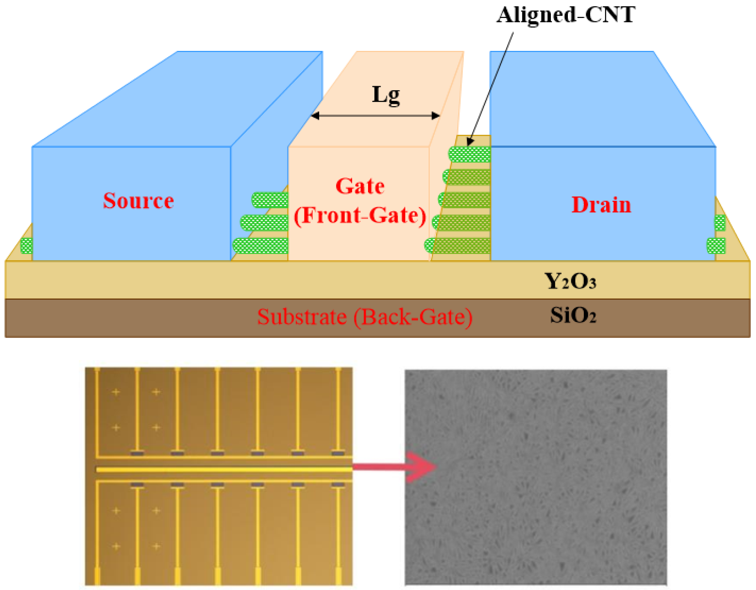
Figure 2.
Current-voltage characteristics of P-CNTFET.
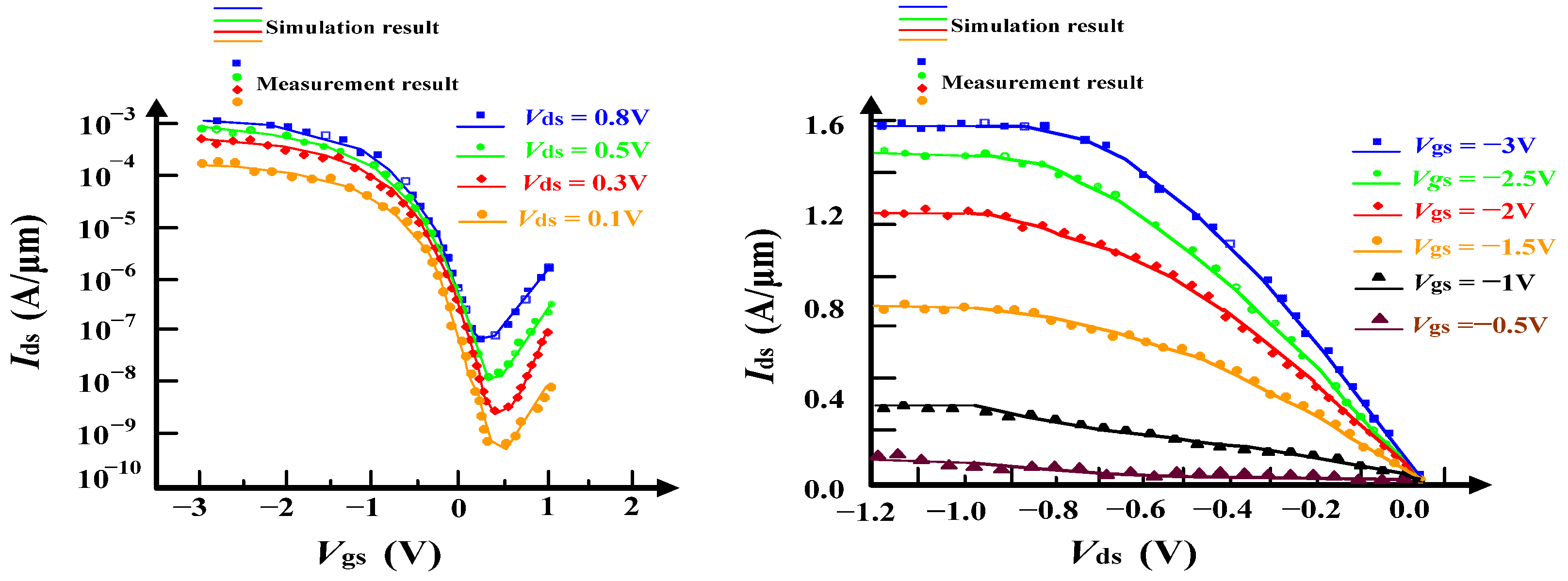
Figure 3.
W/L = 1 μm/500 nm P-CNTFET fitting results: (a) linear coordinates; (b) logarithmic coordinates.
Figure 3.
W/L = 1 μm/500 nm P-CNTFET fitting results: (a) linear coordinates; (b) logarithmic coordinates.
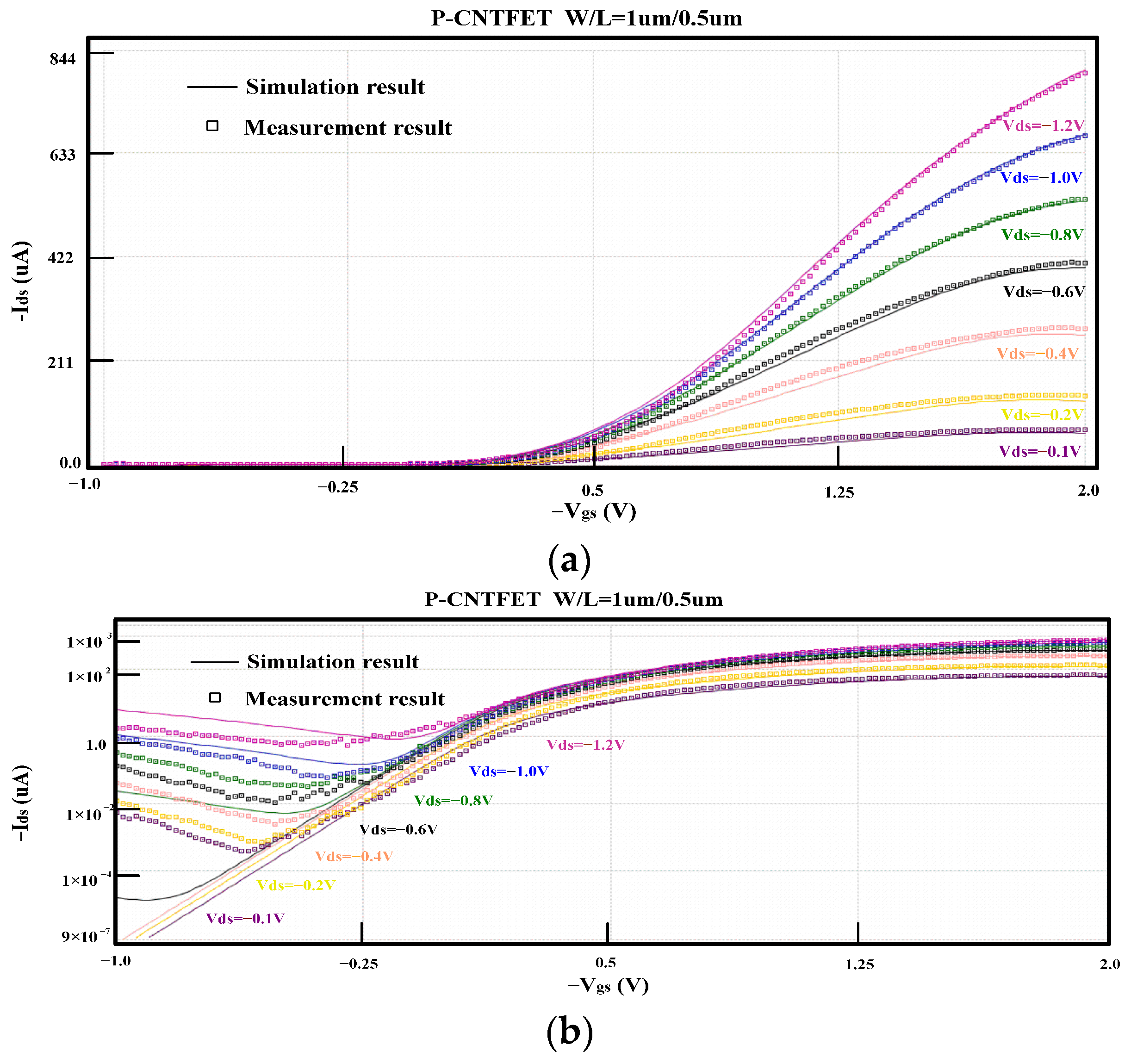
Figure 4.
CNTFET PDK design flow.
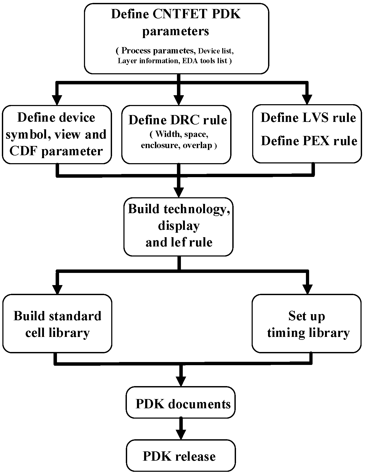
Figure 5.
L/E-type P-CNTFET and layer information: (a) L-type P-CNTFET; (b) E-type P-CNTFET.
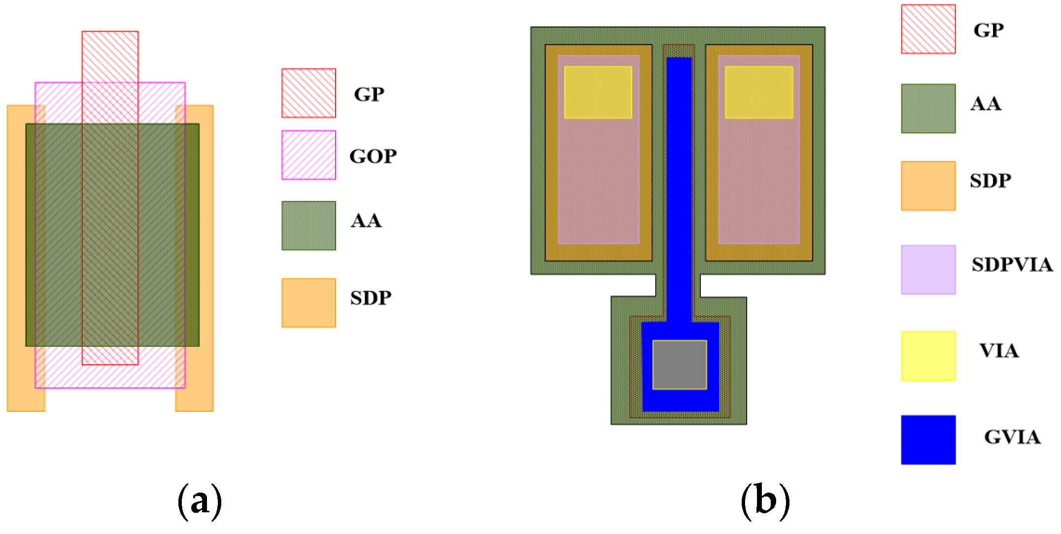
Figure 6.
L-type P-CNTFET DRC rule definition.
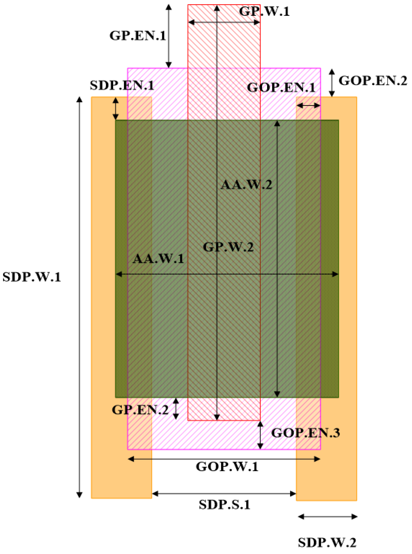
Figure 7.
Layout of DFXD1.
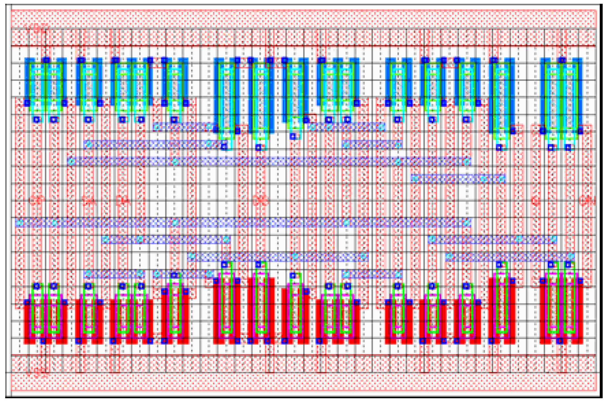
Figure 8.
Layout of full adder FA1D0.

Figure 9.
P-CNTFET (W/L = 1 μm/1 μm): (a) output characteristics; (b) transfer characteristics.
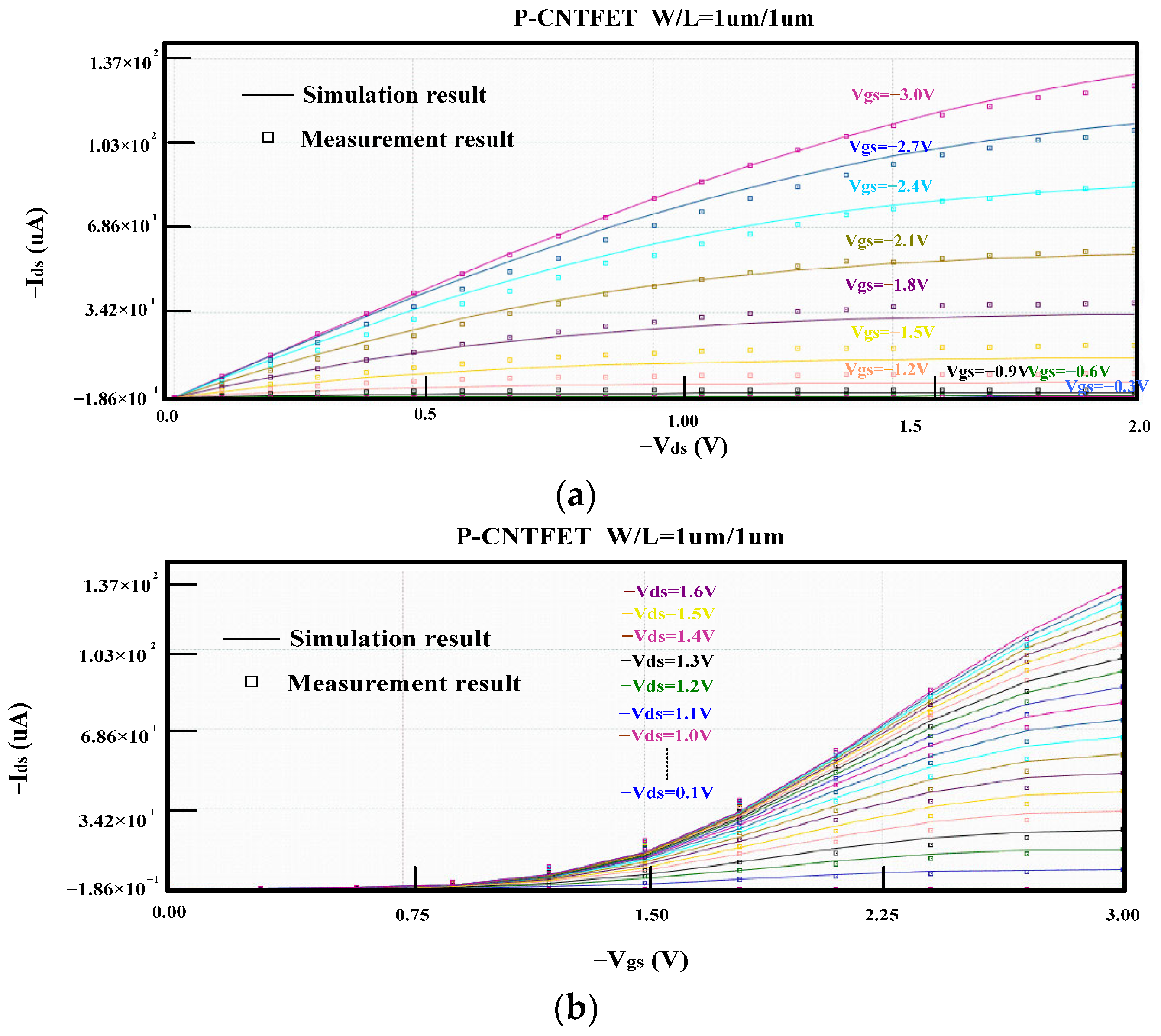
Figure 10.
N-CNTFET (W/L = 1 μm/1 μm): (a) output characteristics; (b) transfer characteristics.
Figure 11.
Schematic and layout of two-stage CNTFET operational amplifier.
Figure 12.
Pre-/post-AC simulation results of operational amplifier.

Figure 13.
6T SRAM cell and layout of 8 × 8 array.

Figure 14.
Read/write function and SNM of SRAM.

Figure 15.
Layout of 8-bit counter.

Table 1.
Model parameter definitions.
| Parameter | Description |
|---|---|
| Lch | Channel length |
| Lgeff | Mean free path in the channel region of intrinsic CNTFET with imperfect elastic scattering |
| Lss | Source-extended region length of CNTFET |
| Ldd | Drain-extended region length of CNTFET |
| Efi | Fermi energy |
| Kgate | Dielectric constant of high-K top-gate dielectric material |
| Tox | Thickness of high-K top-gate dielectric material |
| Csub | Coupling capacitor between channel and back-gate (back-gate effect) |
| Ccsd | Coupling capacitor between channel and source/drain region |
| CoupleRatio | Percentage of Ccsd corresponding to the coupling capacitor between channel and drain |
| Vfbn, Vfbp | Flat band voltage of N-CNTFET and P-CNTFET |
| Pitch | Distance between centers of two adjacent CNTs in the device |
| CNTPos | Position of carbon nanotubes under gate |
| n1, n2 | Chirality of CNTFET |
| tubes | Number of carbon nanotubes in device |
| coeffvg0, coeffvg1, coeffvg2 | Fitting parameters |
Table 2.
Layer definition.
| Layer | Definition |
|---|---|
| GP | P gate |
| GOP | P gate oxygen |
| AA | Active area |
| SDP | P source–drain contact |
| SDPVIA | VIA of drain and source |
| VIA | Standard VIA |
| GVIA | VIA of gate |
Table 3.
L-type P-CNTFET DRC rule description.
| DRC Rule | Description | Dimension (nm) |
|---|---|---|
| GP.W.1 | P gate length | ≥90 |
| GP.W.2 | P gate width | ≥110 |
| GOP.W.1 | P gate oxide width | ≥175 |
| GOP.EN.1 | Horizontal extension of P gate oxide to SDP | 15 |
| GOP.EN.2 | Vertical extension of P gate oxide to SDP | 50 |
| GOP.EN.3 | Extension of P gate oxide to GP | 50 |
| AA.W.1 | Horizontal width of AA | ≥500 |
| AA.W.2 | Vertical width of AA | ≥200 |
| SDP.W.1 | Horizontal width of SDP | ≥700 |
| SDP.W.2 | Vertical width of SDP | ≥80 |
| SDP.S.1 | Space between SDP | ≥95 |
| SDP.EN.1 | Extension of SDP to AA | 50 |
Table 4.
The 90 nm CNTFET standard cell library.
| Category | Description | #Cells |
|---|---|---|
| Combinational | INVDx, BUFFDx, BUFTDx, ND2Dx, NR2Dx, AN2Dx, OR2Dx, XNR2Dx, XOR2Dx | 18 |
| Complex Logic | AO211Dx, OA211Dx, AOI211Dx, IAO21Dx, IOA21Dx, OAI211Dx, MUX2Dx, MUX2NDx | 16 |
| Latch | LHCNDx, LNCNDx | 4 |
| Flip-Flop | DFXDx | 2 |
| Scan Cell | SDFDx, SDFKCNDx | 2 |
| Delay Cell | DELx | 2 |
| Clock Buffer | CKBDx, CKNDx | 2 |
| Adder | FA1Dx, HA1Dx | 2 |
| Tie-High/Tie-Low Cell | TIEH, TIEL | 2 |
| Filler Cell for Core | FILL | 2 |
| Decoupling Cell | DCAPx | 2 |
Table 5.
Performance comparison of CNTFET compact model.
| Parameter | [18] | [22] | [23] | [34] | This Work |
|---|---|---|---|---|---|
| Technology (nm) | 32 | 9 | 15 | 200 | 90 |
| Gate structure | dual gate | single gate | single gate | dual gate | dual gate |
| Simulation tool | HSPICE | HSPICE | HSPICE | HSPICE | HSPICE |
| Method | numerical analysis | semi-analytical | virtual source (VS) | numerical analysis | numerical analysis |
| Convergence | good | good | good | good | good |
| Characteristics | quantum confinement, scattering, screening effect | contact resistance modeling, tunneling | effective mobility, inverse subthreshold slope degradation, quantum capacitance | Schottky barrier, electrostatic modeling, tunneling | back-gate effect, transmission probability, tunneling |
Table 6.
Standard cell used for 8-bit counters.
| Standard Cell | Description | #Cells |
|---|---|---|
| HA1D0 | Full adder | 6 |
| INVD0 | Inverter | 1 |
| XOR2D1 | XOR gate | 1 |
| DFXD1 | Flip-flop | 8 |
Disclaimer/Publisher’s Note: The statements, opinions and data contained in all publications are solely those of the individual author(s) and contributor(s) and not of MDPI and/or the editor(s). MDPI and/or the editor(s) disclaim responsibility for any injury to people or property resulting from any ideas, methods, instructions or products referred to in the content. |
© 2024 by the authors. Licensee MDPI, Basel, Switzerland. This article is an open access article distributed under the terms and conditions of the Creative Commons Attribution (CC BY) license (https://creativecommons.org/licenses/by/4.0/).
Share and Cite
MDPI and ACS Style
Chen, L.; Zhang, Y.; Chen, Z.; Chen, J.; Chen, H.; Jiang, J.; Chen, C. Full-Custom 90 nm CNTFET Process Design Kit: Characterization, Modeling, and Implementation. Electronics 2024, 13, 605. https://doi.org/10.3390/electronics13030605
AMA Style
Chen L, Zhang Y, Chen Z, Chen J, Chen H, Jiang J, Chen C. Full-Custom 90 nm CNTFET Process Design Kit: Characterization, Modeling, and Implementation. Electronics. 2024; 13(3):605. https://doi.org/10.3390/electronics13030605
Chicago/Turabian StyleChen, Liming, Yuyan Zhang, Zhifeng Chen, Jiming Chen, Huangwei Chen, Jianhua Jiang, and Chengying Chen. 2024. "Full-Custom 90 nm CNTFET Process Design Kit: Characterization, Modeling, and Implementation" Electronics 13, no. 3: 605. https://doi.org/10.3390/electronics13030605
Note that from the first issue of 2016, this journal uses article numbers instead of page numbers. See further details here.