Article

Area-Power-Delay-Efficient Multi-Modulus Multiplier Based on Area-Saving Hard Multiple Generator Using Radix-8 Booth-Encoding Scheme on Field Programmable Gate Array

Department of Electrical Engineering, National Quemoy University, Kinmen 89250, Taiwan
*
Author to whom correspondence should be addressed.
Electronics 2024, 13(2), 311; https://doi.org/10.3390/electronics13020311
Submission received: 6 December 2023 / Revised: 5 January 2024 / Accepted: 8 January 2024 / Published: 10 January 2024

Abstract

:
A multi-modulus architecture based on the radix-8 Booth encoding of a modulo (2n − 1) multiplier, a modulo (2n) multiplier, and a modulo (2n + 1) multiplier is proposed in this paper. It uses the original single circuit and shares many common circuit characteristics with a small extra circuit to carry out multi-modulus operations. Compared with a previous radix-4 study, the radix-8 architecture can increase the modulation multiplication encoding selection from three codes to four codes. This reduces the use of partial products from ⌊n/2⌋ to ⌊n/3⌋ + 1, but it increases the operation complexity for multiplication by three circuits. A hard multiple generator (HMG) is used to address this problem. Two judgment signals in the multi-modulus circuit can be used to perform three operations of the modulo (2n − 1) multiplier, modulo (2n) multiplier, and modulo (2n + 1) multiplier at the same time. The weighted representation is used to reduce the number of partial products. Compared with previously reported methods in the literature, the proposed approach can achieve better performance by being more area-efficient, being faster, consuming low power, and having a lower area-delay product (ADP) and power-delay product (PDP). With the multi-modulus HMG, the proposed modified architecture can save 34.48–55.23% of hardware area. Compared with previous studies on the multi-modulus multiplier, the proposed architecture can save 22.78–35.46%, 4.12–11.15%, 12.59–24.73%, 27.88–38.88%, and 20.49–27.85% of hardware area, delay time, dissipation power, ADP, and PDP, respectively. Xilinx field programmable gate array (FPGA) Vivado 2019.2 tools and the Verilog hardware description language are used for synthesis and implementation. The Xilinx Artix-7 XC7A35T-CSG324-1 chipset is adopted to evaluate the performance.

1. Introduction

In recent decades, the residue number system (RNS) [1,2,3,4,5,6] has been increasingly applied in cryptography [2,7], error correction codes [8], and digital signal processing [3], owing to its carry-free nature and parallel computation. A reduced power consumption, shorter latency, and smaller hardware area can be achieved for applications based on RNS modulation addition [9,10,11,12,13] and multiplication [14,15,16,17,18,19,20,21,22,23,24,25]. When using the multi-modulus architecture, multiple modulus operations can be performed at the same time. Many common hardware circuits can share in the multi-modulus architecture of modulo (2n − 1), modulo (2n), and modulo (2n + 1) multipliers, owing to the commonality of the modulus and similarity of hardware circuits in the modulo multiplication, so only different modules of the circuit need to be additionally designed, which significantly reduces the circuit area. Diminished-1 representation [9,11,12] and weighted representation [13,25] are the two main representations in the RNS-based modulo multiplier. A weighted representation is adopted in the current work.
The traditional modified Booth-encoded multiplier is also called a radix-4 Booth-encoded multiplier [20,25,26], which uses a three-code interpretation. A 0 is added after the least significant bit (LSB), and a 0 is also added in front of the most significant bit (MSB) of the multiplier, which then encodes it in groups of three bits, so that only ⌊n/2⌋ are needed for partial products with n bits. This leads to a reduction in the use of full adders and greatly reduces the circuit area and delay time. Compared with the previous radix-4 research, the radix-8 [20,22,23,24] architecture can increase the modulation multiplication encoding selection from a three-code to a four-code interpretation, which reduces the use of partial products from ⌊n/2⌋ to ⌊n/3⌋ + 1. As the three-code interpretation (radix-4 multiplier) increases to a four-code interpretation (radix-8 multiplier), the partial product is reduced from half of the traditional multiplier to one-third, which further improves the circuit area and delay time. The radix-4-based multiplicand in the three-code interpretation is only multiplication by 1 (×1) and multiplication by 2 (×2). Through the carry-free principle in the RNS, the multiplication by 2 (×2) multiplicand only needs to return the original multiplicand once (shift left by one bit). However, for the radix-8 multiplier, there will be an additional multiplication by 3 (×3) and multiplication by 4 (×4) operations to be processed. The multiplication by 4 (×4) operation can use the same carry-free principle in the RNS to return twice (shift left by 2 bits). However, multiplication by 3 (×3), which is processed by the hard multiple generator (HMG), needs to be obtained by adding multiplication by 1 (×1) and multiplication by 2 (×2) of the original multiplicand. This increases the cost of the hardware area, delay, and power consumption. Therefore, simplifying the HMG for a triple operation is very important. An area-saving modified multi-modulus HMG is first presented for this proposed multi-modulus multiplier.
The proposed architecture of the multi-modulus multiplier based on an area-saving HMG using a radix-8 Booth-encoding scheme can achieve significant improvements in hardware cost, delay time, and power consumption. The structure of the area-delay-power-efficient multi-modulus multiplier proposed in this paper can operate the modulo (2n − 1), modulo (2n), and modulo (2n + 1) multipliers at the same time with only two control signals sharing the same hardware structure. The proposed multi-modulus HMG circuit and modular multiplication can also greatly reduce the hardware cost compared to that of Rama’s [20] method. For FPGA implementation, there are many FPGA families and many manufacturers. The propagation time in the LUT (Look-Up Table)/ALM (Adaptive Logic Module) array is different in Xilinx Artix-7, Xilinx Spartan-7, Xilinx Kintex-7, Intel Cyclone-10, and so on. In the proposed work, the Xilinx Artix-7 XC7A35T-CSG324-1 chipset is adopted to evaluate the performance.
The rest of this paper is organized as follows. The methods reported in the literature are described in Section 2. Section 3 presents the proposed multi-modulus HMG and radix-8 Booth-encoding-based multi-modulus multiplier design, which is area-delay-power efficient. The results of the proposed scheme in comparison with those of various other methods are presented in Section 4. Finally, Section 5 concludes the study.

2. Previous Work

2.1. Radix-8 Multi-Modulus Multiplier in {2n − 1, 2n, 2n + 1}

A structure in which a multi-modulus multiplier can be operated under the same hardware architecture has been reported [20]. This design can greatly reduce the area used. There are three types of modulus multiplication, namely, modulo (2n − 1), modulo (2n), and modulo (2n + 1) multipliers, which can be processed using two control signals. Let X be the multiplicand, Y the multiplier and Z the binary product. Weighted representation is used for modulo m, m = 2n − 1, or 2n; diminish-1 representation is used for m = 2n + 1, where m is the modulo parameter. The general expression is as follows [20]:
| Z | m = { | X Y | m                               i f   m = 2 n 1   or   2 n | X Y + X + Y | m                     i f   m = 2 n + 1
where | X Y | m is denoted as the modulo m residue of X Y .
The partial product (PP) can be obtained after taking radix-8 operations of X and Y. The related equation is expressed as [20]:
| Z | m = { | i = 0 n / 3 P P i | m                                                                   i f   m = 2 n 1 | i = 0 n / 3 P P i + i = 0 n / 3 K i | m                                   i f   m = 2 n | i = 0 n / 3 P P i + i = 0 n / 3 K i + X + Y | m       i f   m = 2 n + 1
where Ki is the extra compensation parameter. The complete equation of Ki, where KDi is a dynamic bias and KSi is a static bias, is as follows [20]:
i = 0 n / 3 K i = i = 0 n / 3 2 3 i ( m 2 i + m 4 i ¯ ) + ( m 3 i + m 4 i ¯ ) 2 3 i + 1 + 2 3 i + 1 s i + K D i i = 0 n / 3 ( ( m 2 i + m 4 i ) s i ) 2 3 i + 1 + ( ( m 3 i + m 4 i ) s i ) 2 3 i + 2 K D i + i = 0 n / 3 2 3 i 2 3 i + 1 K D i 2 3 i + 1 K S i
where m2i, m3i, m4i denote the ith partial product row of multiplication by 2 bits, multiplication by 3 bits, and multiplication by 4 bits, respectively.
The value of the carry bit (ci) for an even carry bit (Equation (4)) and an odd bit (Equation (5)) are given by [19]:
c i = { ( g i , p i ) ( g i 2 , p i 2 ) ( g 0 , p 0 ) ( g n 2 , p n 2 ) ( g i + 2 , p i + 2 ) ; i f   m = 2 n 1 ( g i , p i ) ( g i 2 , p i 2 ) ( g 0 , p 0 ) ( 0 , 0 ) ( 0 , 0 ) ; i f   m = 2 n ( g i , p i ) ( g i 2 , p i 2 ) ( g 0 , p 0 ) ( p n 2 ¯ , g n 2 ¯ ) ( p i + 2 ¯ , g i + 2 ¯ ) ; i f   m = 2 n + 1
and:
c i = { ( g i , p i ) ( g i 2 , p i 2 ) ( g 1 , p 1 ) ( g n 1 , p n 1 ) ( g i + 2 , p i + 2 ) ; i f   m = 2 n 1 ( g i , p i ) ( g i 2 , p i 2 ) ( g 1 , p 1 ) ( 0 , 0 ) ( 0 , 0 ) ; i f   m = 2 n ( g i , p i ) ( g i 2 , p i 2 ) ( g 1 , p 1 ) ( p n 1 ¯ , g n 1 ¯ ) ( p i + 2 ¯ , g i + 2 ¯ ) ; i f   m = 2 n + 1
respectively, where (gi*, pi*) is defined as a modified generated–propagated bit pair and (gi*, pi*) (gj*, pj*) = (gi*+ pi* gj*, pi* pj*).
For the final adder of this study, a Sklansky-based parallel prefix adder [13] is used. The study presents multi-modulus modulo (2n − 1), modulo (2n), and modulo (2n + 1) multipliers [20] that can reuse the same hardware resources. Nevertheless, the performance of the hardware area, latency, and power consumption still have room for improvement. The improved method and hardware structure are discussed in the next section.

2.2. Hard Multiple Generators

This subsection discusses the HMG for the modulo (2n − 1) [22], modulo (2n) [23], and modulo (2n + 1) [24] multipliers in the literature. In the Booth encoder (BE), the radix-8 Booth-encoding operation, which can reduce the number of partial products to ⌊n/3⌋ + 1 items by means of a four-bit interpretation of the multiplier; multiplication by 1 ( × 1); multiplication by 2 ( × 2); multiplication by 3 ( × 3); multiplication by 4 ( × 4); and the sign signal is obtained after the operation. Multiplications by 1 ( × 1), 2 ( × 2), and 4 ( × 4) are easy to handle, as multiplications by 2 ( × 2) and 4 ( × 4) only need to shift one bit and two bits to the left, respectively. However, multiplication by 3 ( × 3) is difficult to handle and cannot be obtained directly from the multiplicand, so the HMG unit is used to operate the process.
There are two processing methods; the first is |+X|m + |+2X|m, and the second is |−X|m + |+4X|m, where X is the multiplicand and |X|m is defined as the modulo operation of X. The first type is clearly better than the second type because the first one does not need to process the 1’s compliment operation. The related derivation results of the reported HMG are as follows. The representation of multiplication by 3 ( × 3) is as follows:
| + 3 X | m = | + X | m + | + 2 X | m ; | + X | m = ( x n 1 x n 2 x 0 ) ; | + 2 X | m = { ( x n 2 x n 3 x 0 x n 1 ) ,   i f   m = 2 n 1 ( x n 2 x n 3 x 0 0 ) ,   i f   m = 2 n   ;
The generated bit, propagated bit, half sum bit, and delay half (DH) sum bit are defined as gi, pi, hi, and dhi, respectively [22,23,24]:
g i = x i   x i 1 p i = x i + x i 1 h i = x i x i 1 d h i = x 2 i + 1 x 2 i h 2 i
The equation for the carry bit at the odd position is shown as [22,23,24]:
c 2 i 1 = P 2 i 1 H 2 i 1
where P 2 i 1 is a modified propagated bit, and H 2 i 1 is a modified Ling bit [22,23,24]. The general equation of the modified Ling bit H 2 i 1 is represented as [22,23,24]:
H 2 i 1 = ( G 2 i 1 , P 2 i 3 ) ( G 2 i 5 , P 2 i 7 ) ( G 2 i 9 , P 2 i 11 )
where G 2 i 1 and P 2 i 1 are modified G 2 i 1 and modified P 2 i 1 bits, respectively. H 2 i 1 is used to produce odd carry bits in the HMG and perform HMG prefix operations between G 2 i 1 and H 2 i 1 . G 2 i 1 and P 2 i 1 are used to perform the logic OR operation and logic AND operation for the modified generated bit ( G 2 i 1 ) and modified propagated bit ( P 2 i 1 ), respectively. The modified generated bit ( G 2 i 1 ) and modified propagated bit ( P 2 i 1 ) are calculated from the generated bit and propagated bit, respectively. H 2 i 1 , G 2 i 1 , and P 2 i 1 are the intermediate processing units in the HMG operation and can be used to produce the hard multiple bit. The final equation for the sum of bits at the even and odd positions in the HMG is as follows [22,23,24]:
s 2 i = h i ( P 2 i 1 H 2 i 1 ) s 2 i + 1 = d h i ( h 2 i ( P 2 i 1 H 2 i 1 ) )
From the above derivation of Equations (6)–(10), the block diagram is HMG was presented [22,23,24].
The proposed multi-modulus HMG structure for three types of modulo (2n − 1), modulo (2n), and modulo (2n + 1) multipliers based on radix-8 operation using the same hardware circuit is presented in the next section.

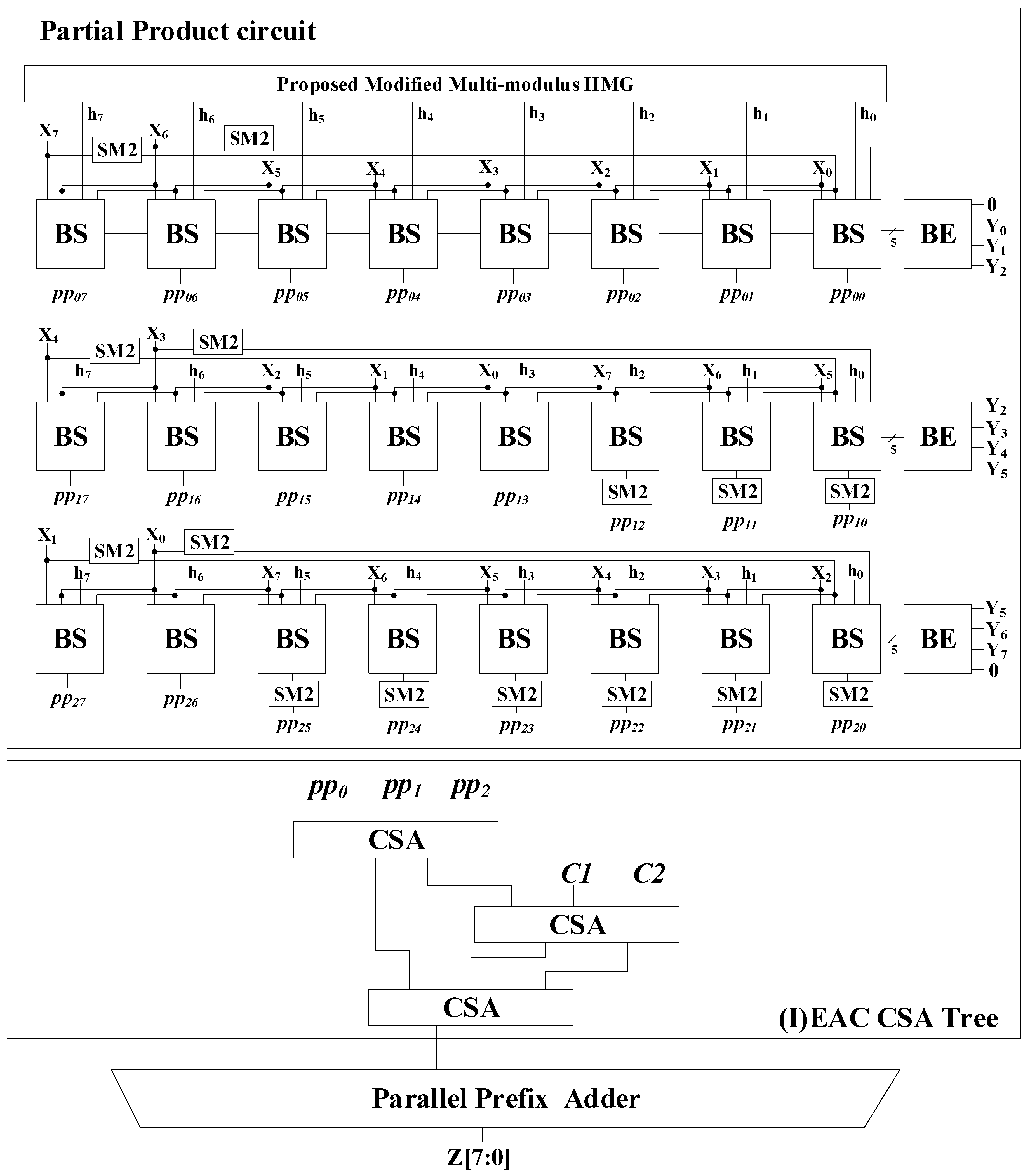
3. Proposed Multi-Modulus Multiplier Based on Radix-8 Booth Encoding

Figure 1 shows a block diagram of the system architecture of the proposed multi-modulus multiplier based on an area-saving HMG using a radix-8 Booth-encoding scheme. Multi-modulus multipliers are defined to support modulo (2n − 1), modulo (2n), and modulo (2n + 1) multiplication functions in the same circuit hardware by the control signal (S1, S0). When (S1, S0) = (0, 0), the modulo (2n − 1) multiplier operation is selected; when (S1, S0) = (0, 1), the modulo (2n) multiplier operation is selected; and when (S1, S0) = (1, 0), the modulo (2n + 1) multiplier operation is selected. In Figure 1, the proposed multi-modulus multiplier includes the Booth encoder (BE) unit, hard multiple generator (HMG) unit, Booth selector (BS) unit, compensation unit, an inverse end-around-carry carry-save adder tree (IEAC CSA tree), and the proposed improved parallel prefix adder unit. The multiplier is Booth-encoded by 4 bits to generate × 1, × 2, × 3, × 4, and s signals. Such an encoding can reduce the number of partial products. The multiplicand, +2X (one left shift), +4X (two left shift), and +3X are generated by the HMG. They then enter the BS unit and are selected by the output of the Booth encoder and obtain the output of the ith-row partial product (pp). Afterwards, the partial product (pp) and compensation value C1 and C2 from the compensation circuit are fed into the IEAC CSA tree and summed to obtain sum (S) and carry (C). Finally, the obtained S and C are summed through the final parallel prefix adder to obtain the product O. The proposed multi-modulus HMG and proposed radix-8 multi-modulus multiplier are discussed in the following subsection.

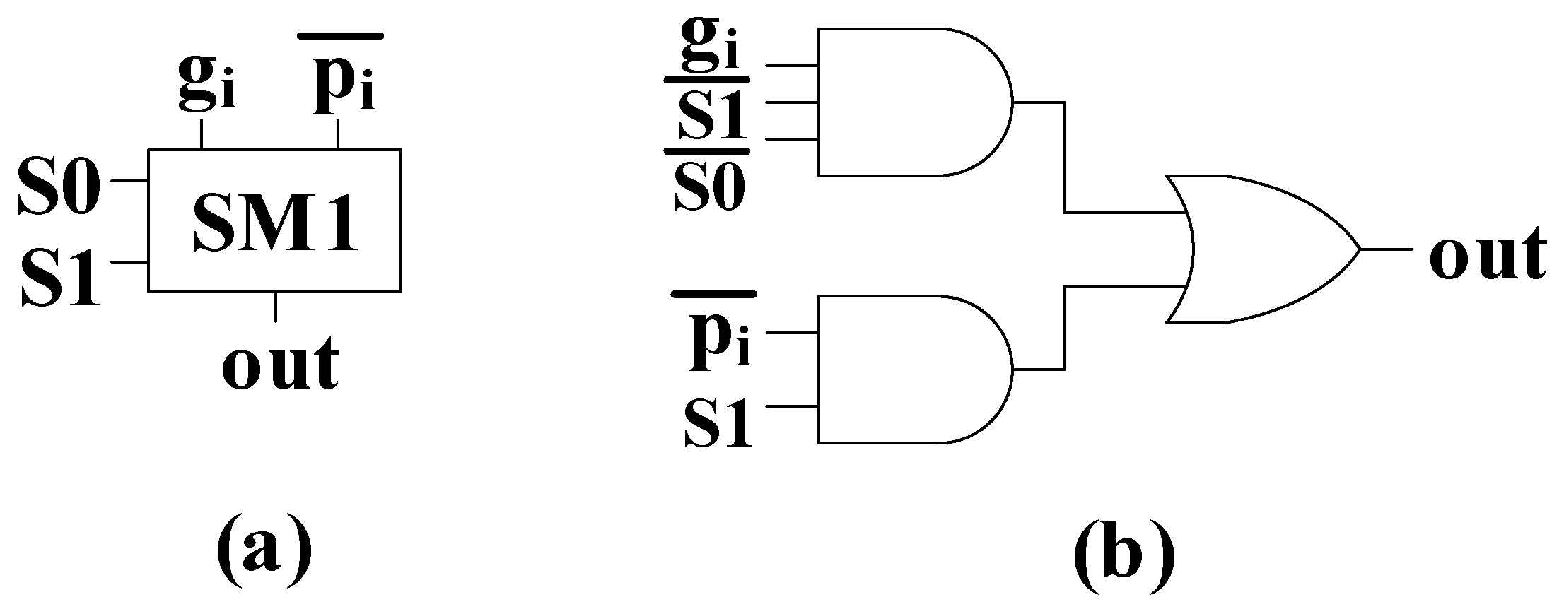
3.1. Proposed Multi-Modulus Hard Multiple Generator

In this subsection, the modified multi-modulus HMG for the modulo (2n − 1), modulo (2n), and modulo (2n + 1) multiplier operations is discussed. The proposed structure of radix-8 multi-modulus HMG (n = 8) is designed as shown in Figure 2. The proposed structure includes a GP**P* block, DH block, SM1, SM2, prefix operator unit (grey circle), and post-processing unit (grey square, white square, grey diamond, and white diamond).
In Figure 3 and Figure 4, SM1 and SM2 refer to the special multiplexer 1 and special multiplexer 2, respectively. These blocks are used to generate different input signals from the multi-modulus by selecting (S1, S0).
In the block diagram of the GP**P* function, Xi is the input of the multiplicand, Gi* and Pi* are, respectively, the modified generated and propagated bits in the HMG, and Gi** and Pi** are, respectively, the modified Gi* and Pi* bits. The related equations of Gi**, Pi**, Gi*, and Pi* are derived from the modulo (2n − 1) multiplier [22], modulo (2n) multiplier [23], and modulo (2n + 1) [24] multiplier:
{ G i = G i + G i 2   , i f   i = 1   ,   f o r   m = 2 n 1 G i = G i + 0   , i f   i = 1   ,   f o r   m = 2 n G i = G i + P i 2 ¯   , i f   i = 1   ,   f o r   m = 2 n + 1
{ P i = P i P i 2   , i f   i = 1   ,   f o r   m = 2 n 1 P i = P i 0   , i f   i = 1   ,   f o r   m = 2 n P i = P i G i 2 ¯   , i f   i = 1   ,   f o r   m = 2 n + 1
{ G i = G i + G i 2   , i f   1 < i < n   ,   f o r   m = 2 n 1 G i = G i + G i 2   , i f   1 < i < n   ,   f o r   m = 2 n G i = G i + G i 2   , i f   1 < i < n   ,   f o r   m = 2 n + 1
{ P i = P i P i 2   , i f   1 < i < n   ,   f o r   m = 2 n 1 P i = P i P i 2   , i f   1 < i < n   ,   f o r   m = 2 n P i = P i P i 2   , i f   1 < i < n   ,   f o r   m = 2 n + 1
From Equation (11) to Equation (14), when i = 1, Gi* and Pi* can be rewritten as:
{ G 1 = x 0 ( x 1 + x 1 )   ,   f o r   m = 2 n 1 G 1 = x 0 ( x 1 + 0 )   ,   f o r   m = 2 n G 1 = x 0 ( x 1 +   x 1 ¯   )   ,   f o r   m = 2 n + 1
{ P 1 = x 0 + ( x 1   x 1 )   ,   f o r   m = 2 n 1 P 1 = x 0 + ( x 1 0 )   ,   f o r   m = 2 n P 1 = x 0 + ( x 1   x 1 ¯ )   ,   f o r   m = 2 n + 1
From the above definitions of Gi*, Pi*, Gi**, and Pi** for the modulo (2n − 1), modulo (2n), and modulo (2n + 1) multipliers, the block diagram of the proposed GP**P* function is shown in Figure 5. The Pp7* signal is used to select the P 7 , 0, or P 7 ¯ signals for the modulo (2n − 1), modulo (2n), or modulo (2n + 1) multipliers, respectively.
For the DH block, multiplication by 2 ( × 2) for the modulo (2n − 1), modulo (2n), and modulo (2n + 1) multipliers is expressed as:
| + 2 X | m = { ( x n 2 x n 3 x 0 x n 1 )                 i f   m = 2 n 1 ( x n 2 x n 3 x 0 0 )                 i f   m = 2 n ( x n 2 x n 3 x 0 x n 1 ¯ )                 i f   m = 2 n + 1 .
Based on Equations (6) and (7) and Equation (17), the DH component is as shown in Figure 6. In Figure 6a, i = 0 is shown for the end-around-carry bit in the multi-modulus. Figure 6b is the general circuit implementation for i > 0.
In the prefix operator block, H 2 i 1 (i = 1, 2, 3,…) is the modified Ling bit and is expressed at odd positions, which is defined as H 2 i 1 = ( G 2 i 1 ,   P 2 i 3 ) ( G 2 i 5 ,   P 2 i 7 ) , where H 1 = H n 1 , G i = G n i , and P i = P n i [22,23,24]. Taking n = 8 as an example, H 2 i 1 can be shown as Equation (18). The index of H 2 i 1 at position 1 and position 5 is different from the index of H 2 i 1 at position 3 and position 7. Therefore, H 2 i 1 is separated into two groups: H 4 k + 1 and H 4 k + 3 [24], where k = 0, 1, 2, 3, …. That is to say, H 2 i 1 = ( H 1 , H 3 , H 5 , H 7 , H 9 , H 11 …) is divided into two groups: H 4 k + 1 = ( H 1 , H 5 , H 9 …) and H 4 k + 3 = ( H 3 , H 7 , H 11 …). The general expressions of H 2 i 1 for modulo (2n − 1), modulo (2n), and modulo (2n + 1) are derived from the modulo (2n − 1) multiplier [22], modulo (2n) multiplier [23], and modulo (2n + 1) multiplier [24], respectively:
H 1 = ( G 1 ,   G ¯ 7 ) ( P ¯ 5 ,   G ¯ 3 ) H 3 = ( G 3 ,   P 1 ) ( P ¯ 7 ,   G ¯ 5 ) H 5 = ( G 5 ,   P 3 ) ( G 1 ,   G ¯ 7 ) H 7 = ( G 7 ,   P 5 ) ( G 3 ,   P 1 )
{ H 4 k + 1 = ( G 4 k + 1 , P 4 k 1 ) ( G 1 , P 1 ) ( G 4 k 3 , P 4 k 5 ) n 4 H 4 k + 3 = ( G 4 k + 3 , P 4 k + 1 ) ( G 3 , P 1 ) ( G 4 k 1 , P 4 k 3 ) n 4 , f o r   modulo   ( 2 n 1 )
{ H 4 k + 1 = ( G 4 k + 1 , P 4 k 1 ) ( G 1 , 0 ) ( 0 , 0 ) n 4 H 4 k + 3 = ( G 4 k + 1 , P 4 k 1 ) ( G 3 , P 1 ) ( 0 , 0 ) n 4 , f o r   modulo   2 n
{ H 4 k + 1 = ( G 4 k + 1 , P 4 k 1 ) ( G 1 , G 1 ¯ ) ( P 4 k 3 ¯ , G 4 k 5 ¯ ) n 4 H 4 k + 3 = ( G 4 k + 3 , P 4 k + 1 ) ( G 3 , P 1 ) ( P 4 k 1 ¯ , G 4 k 3 ¯ ) n 4 , f o r   modulo ( 2 n + 1 )
From Equation (9) and the description of H 2 i 1 above, the relative logic circuit is obtained as shown in Figure 7.
For the post-processing unit, the block diagrams of the grey square, white square, grey diamond, and white diamond are shown in Figure 8 and Figure 9. For i = 0, the circuit implementation of the even-position sum bit and odd-position sum bit is designed as shown in Figure 8a,b, respectively. For i > 0, the circuit implementation of the even-position sum bit and odd-position sum bit is designed as shown in Figure 9a,b, respectively.
The final results of the HMG for the sum bit are expressed as follows. The equations for the even-position sum bit and odd-position sum bit for i = 0 are expressed as Equations (22) and (24), respectively, and the equations for the even-position sum bit and odd-position sum bit for i > 0 are expressed as Equations (23) and (25), respectively:
{ s 2 i = h 2 i ( P 2 i 1 H 2 i 1 ) , i f   i = 0   ,   f o r   m = 2 n 1 s 2 i = h 2 i 0 , i f   i = 0   ,   f o r   m = 2 n s 2 i = h 2 i ( P 2 i 1 ¯ + H 2 i 1 ¯ )   , i f   i = 0   ,   f o r   m = 2 n + 1
{ s 2 i = h 2 i ( P 2 i 1 H 2 i 1 ) , i f   0 < i < n / 2   ,   f o r   m = 2 n 1 s 2 i = h 2 i ( P 2 i 1 H 2 i 1 ) , i f   0 < i < n / 2   ,   f o r   m = 2 n s 2 i = h 2 i ( P 2 i 1 H 2 i 1 ) , i f   0 < i < n / 2   ,   f o r   m = 2 n + 1
{ s 2 i + 1 = d h i ( P 2 i 1 H 2 i 1 ) h 2 i , i f   i = 0   ,   f o r   m = 2 n 1 s 2 i + 1 = d h i 0 h 2 i , i f   i = 0   ,   f o r   m = 2 n s 2 i + 1 = d h i ( P 2 i 1 ¯ + H 2 i 1 ¯ ) h 2 i , i f   i = 0   ,   f o r   m = 2 n + 1
{ s 2 i + 1 = d h i ( P 2 i 1 H 2 i 1 ) h 2 i , i f   0 < i < n / 2   ,   f o r   m = 2 n 1 s 2 i + 1 = d h i ( P 2 i 1 H 2 i 1 ) h 2 i , i f   0 < i < n / 2   ,   f o r   m = 2 n s 2 i + 1 = d h i ( P 2 i 1 H 2 i 1 ) h 2 i , i f   0 < i < n / 2   ,   f o r   m = 2 n + 1
From the above design of the sub-circuit in the HMG, the proposed structure of the radix-8 multi-modulus HMG (n = 8) can be designed as shown in Figure 2. It should be noted that Equation (11) to Equation (16), Equation (18) to Equation (21), and Equation (22) to Equation (25) are integrated and modified equations from the modulo (2n − 1) [22], modulo (2n) [23], and modulo (2n + 1) multipliers [24].

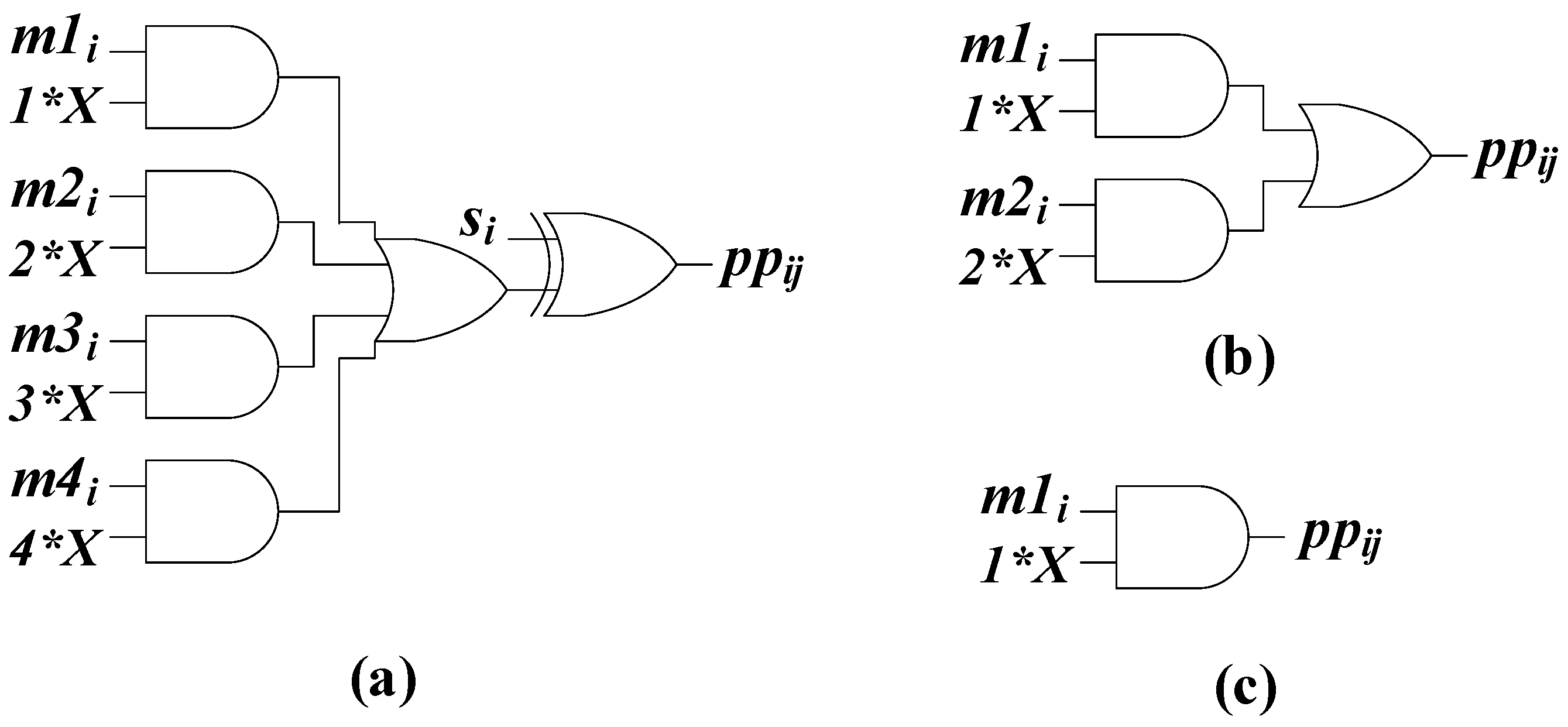
3.2. Proposed Radix-8 Multi-Modulus Multiplier

In this subsection, the proposed radix-8 multi-modulus multiplier is discussed. Let X be the multiplicand and Y the multiplier. The modulo m of X × Y is expressed as | X × Y | m . Using the representation of radix-8, Y can be expressed as Y = 23i(y3i −1 + y3i + 2y3i +1 − 4y3i +2), and the modulo m of X × Y can be expressed as:
| X × Y | m = | X × 2 3 i ( y 3 i 1 + y 3 i + 2 y 3 i + 1 4 y 3 i + 2 | m
The truth table of the four-codes interpretation based on radix-8 is presented in Table 1 [20]. The multiplication by 1 ( × 1), multiplication by 2 ( × 2), multiplication by 3 ( × 3), multiplication by 4 ( × 4), and sign signal are obtained from the BE circuit, which is shown in Figure 10 [20]. The BS is designed as shown in Figure 11a based on the corresponding signals from the BE. In order to reduce the gate count of the BS in the ( n / 3 + 1)th row, when n = 6k + 4 and n = 6k, where k is a positive integer, the BE of the { n / 3 + 1}th row is [Y3i −1 Y3i −2 0 0] and [Y3i −1 0 0 0], the BS can be redesigned as shown in Figure 11b,c, respectively. The hardware area can be effectively reduced as shown in Figure 11b,c. In the BS block, the input signal is multiplication by 1 ( × 1), multiplication by 2 ( × 2), multiplication by 3 ( × 3), multiplication by 4 ( × 4), and the sign bit (s). Multiplication by 2 ( × 2) and multiplication by 4 ( × 4) shift one bit and two bits of the original signal to the left, respectively. Multiplication by 3 ( × 3) is produced from the proposed multi-modulus HMG structure. The sign bit is used to produce the positive or negative multiple. The output of the BS block is the partial product (pp). The end-around-carry is operated based on modulo { 2 n 1 ,   2 n ,   2 n + 1 } = { x 1 ,   0 ,   x 1 ¯ } regulation. SM2 (S1, S0), as depicted in Figure 4, is used to select the modulo multiplier, which is (S1, S0) = {00, 01, 10} = modulo { 2 n 1 ,   2 n ,   2 n + 1 } = { p p ,   0 ,   p p ¯ } . A weighted representation of the system structure is adopted for the proposed modulo (2n − 1), modulo (2n), and modulo (2n + 1) multipliers.
For the modulo (2n + 1) multiplier, the compensation value is used to compensate for the general output of the partial product. The compensation circuit that produces the compensation value of C1 and C2 in the proposed approach is discussed below. From Equation (3), the compensation for circuit Ki can be rewritten as follows and divided into two parts, denoted as C 1 (the first two rows of the equation) and C 2 :
  i = 0 n / 3 K i = { i = 0 n / 3 2 3 i ( m 2 i + m 4 i ¯ ) + ( m 3 i + m 4 i ¯ ) 2 3 i + 1 C 1 + i = 0 n / 3 s i ( m 2 i + m 4 i ) 2 3 i + 1 + s i ( m 3 i + m 4 i ) 2 3 i + 2 ( C 1 ) } + { i = 0 n / 3 2 3 i + 1 s i + i = 0 n / 3 2 3 i 2 3 i + 1 2 3 i + 1 C 2 }
From Equation (27), C 2 can be rewritten as:
C 2 = i = 1 n / 3 2 3 i 1 + i = 0 n / 3 2 3 i + 1 s i ¯ + i = 0 n / 3 1 2 3 i + 2 s i
For C 1 in Equation (27), the 23i +1 terms can be summed as:
i = 0 n / 3 [ ( m 3 i + m 4 i ¯ ) K 1 i 2 3 i + 1 + s i ( m 2 i + m 4 i ) K 2 i 2 3 i + 1 ]
where K1i and K2i are defined as ( m 3 i + m 4 i ¯ ) and s i ( m 2 i + m 4 i ) , respectively.
K1i + K2i can be written as:
K 1 i + K 2 i = ( K 1 i K 2 i ) 2 0 + ( K 1 i K 2 i ) 2 1
where “ ” represents the logic Exclusive OR gate, and “ ” represents the logic AND gate.
The (23i+1)th term of K1i + K2i is 0 when (K1i, K2i) = (0, 0) or carry out when (K1i, K2i) = (1, 1). Therefore, the (23i +1)th term can be rewritten as:
i = 0 n / 3 ( m 3 i + m 4 i ¯ ) K 1 i 2 3 i + 1 s i ( m 2 i + m 4 i ) K 2 i 2 3 i + 1
And by merging the (23i +2)th term in Equation (27), it can be rewritten as:
i = 0 n / 3 1 2 3 i + 2 [ ( ( m 3 i + m 4 i ) s i ) ( K 1 i K 2 i ) ]
The exclusive OR logic symbol is used in Equation (32) because (m3i + m4i) and K1i do not appear simultaneously.
In Equation (32), when n = 3k + 2 bits for k = 1, 2, 3, …, the sum of K1i and K2i at the highest bit position in 23i +1 carry out to 23i +2 when (K1i, K2i) = (1, 1). It cannot also be represented for n bits. Therefore, for i = n / 3 , it should appear at the upper bound of i = n / 3 . Taking n = 8 as an example, the upper bound of n / 3 is 2. For the (27)th bit, the sum of K1i and K2i probably carries out to 28. Therefore, merging the (23i +1)th term of C 2 in Equation (28) for C 1 at i = n / 3 yields:
i = n / 3 n / 3 2 3 i + 1 [ ( m 3 i + m 4 i ¯ ) + ( ( m 2 i + m 4 i ) s i ) ]
and for C 2 at i = n / 3 , it yields:
i = n / 3 n / 3 2 3 i + 1 [ s i ¯ ( K 1 i K 2 i ) ]
Here, the weighted representation is adopted to replace the original diminish-1 representation. Therefore, the extra circuit for adding 2 should be processed in the compensation circuit for the modulo (2n + 1) multiplier. Merging the circuit for adding 2 and C 2 in Equation (28), which makes i = 0, the modified value is obtained as follows:
i = 0 0 ( 2 3 i + 1 s i ¯ ) + 2 + i = 0 0 2 3 i + 2 s i = i = 0 0 2 3 i + 1 ( 1 + s i ¯ ) + i = 0 0 2 3 i + 2 s i = i = 0 0 2 3 i + 1 ( s i ¯ 1 ) + i = 0 0 2 3 i + 2 ( s i + 1 )
For the modulo (2n) multiplier, the compensation value is described as follows [20]:
C 1 = i = 0 n / 3 2 3 i s i
According to the derivation in this subsection, for the modulo (2n + 1) multiplier, the final compensation of C1 (replacing C 1 ) can be obtained as follows:
C 1 = i = 0 n / 3 1 2 3 i + 2 [ ( ( m 3 i + m 4 i ) s i ) ( K 1 i K 2 i ) ] + i = 0 n / 3 2 3 i ( m 2 i + m 4 i ¯ ) + { i = 0 n 3 2 3 i + 1 [ ( m 3 i + m 4 i ¯ ) K 1 i ( ( m 2 i + m 4 i ) s i ) K 2 i ] , w h e n   n ( 3 k + 2 )   b i t , k = 1 , 2 , 3 , i = 0 n 3 1 2 3 i + 1 [ ( m 3 i + m 4 i ¯ ) K 1 i ( ( m 2 i + m 4 i ) s i ) K 2 i ] + i = n 3 n 3 2 3 i + 1 [ ( m 3 i + m 4 i ¯ ) + ( ( m 2 i + m 4 i ) s i ) ] , w h e n   n = ( 3 k + 2 )   b i t , k = 1 , 2 , 3 ,
For modulo 2n + 1, the final compensation of C2 (replacing C 2 ) is obtained as follows:
C 2 = i = 1 n / 3 2 3 i 1 + i = 0 0 2 3 i + 1 ( s i ¯ 1 ) + i = 0 0 2 3 i + 2 ( s i + 1 ) + i = 1 n / 3 1 2 3 i + 2 s i + { i = 1 n / 3 2 3 i + 1 s i   ¯ ,   w h e n n ( 3 k + 2 )   b i t , k = 1 , 2 , 3 , i = 1 n / 3 1 2 3 i + 1 s i ¯ + i = n / 3 n / 3 2 3 i + 1 [ s i ¯ ( K 1 i K 2 i ) ] , w h e n n = ( 3 k + 2 )   b i t , k = 1 , 2 , 3 , .
The final result of | Z | m can be represented as:
| Z | m = { | i = 0 n / 3 P P i + C 1 + C 2 | m
The compensation value C2 is only needed to compensate for the modulo (2n + 1) multiplier. Therefore, two input AND gates are used with the selected signal S1 (Mod S1). The compensation value C1 is needed to compensate for the modulo (2n) and modulo (2n + 1) multipliers. The compensation circuit for n = 8 is shown in Figure 12. It should be noted that the modulo (2n − 1) multiplier need not be compensated for by the extra compensation circuit. The final proposed structure of the radix-8 multi-modulus multiplier for 8 bits (n = 8) is shown in Figure 13, which includes a partial product unit, IEAC unit, and parallel prefix adder. The Lander–Fisher [12] structure is used for the improved parallel prefix adder circuit, which is shown in Figure 14 (n = 8).
Taking n = 8 as an example for the proposed multi-modulus multiplier based on radix-8 Booth encoding, Figure 15 shows the operational processes of the proposed modulo (2n − 1), modulo (2n), and modulo (2n + 1) multipliers. For n = 8, for the modulo (2n − 1) multiplication operation with (S1, S0) = (0, 0), A = 141, and B = 221, the final result is 51; for the modulo (2n) multiplication operation with (S1, S0) = (0, 1), A = 141, and B = 221, the final result is 185; and for the modulo (2n +1) multiplication operation with (S1, S0) = (1, 0), A = 141, and B = 221, the final result is 64.
To summarize, this section presents the design for the multi-modulus HMG and proposed a radix-8 Booth-encoding-based multi-modulus multiplier. The experimental results and comparisons of the hardware area, delay time, dynamic power, area-delay product (ADP), and power-delay product (PDP) with other methods reported in the literature are presented in the next section.

4. Experimental Results and Comparison

The proposed structure of the multi-modulus HMG and multi-modulus multipliers based on radix-8 Booth encoding, which is covered in Section 3, is discussed in this section, along with the experimental results and comparison. The proposed multi-modulus HMG structure integrates and improves the HMG used by the modulo (2n − 1) multiplier [22], modulo (2n) multiplier [23], and modulo (2n + 1) multiplier [24] proposed in the reported studies. The area-saving multifunction based on these three moduli is proposed, and it shares the same hardware architecture. The proposed modified multi-modulus HMG can save 34.48–55.23% of hardware area compared with the reported work [20], as shown in Table 2.
The proposed multi-modulus modulo (2n − 1), modulo (2n), and modulo (2n + 1) multiplexers can support the aforementioned modular multiplication functions in the same circuit hardware. By integrating the individual functions of the modulo (2n − 1), modulo (2n), and modulo (2n + 1) multiplexers into a single multi-modulus multiplier, the proposed approach can save 22.78–35.46% of hardware area compared with previous work [20], as tabulated in Table 3. In addition, the proposed approach can reduce delay time by 4.12–11.15% compared with previous work [20], as tabulated in Table 4. The dynamic power consumption can be reduced by 12.59–24.73% of dissipation power compared with previous work [20], as tabulated in Table 5. Moreover, it can save 27.88–38.88% of ADP compared with previous work [20], as shown in Table 6. Finally, it can save 20.49–27.85% of PDP compared with previous work [20], as tabulated in Table 7.
In Table 2 to Table 7, it is clear that the proposed multi-modulus multiplier based on radix-8 Booth encoding achieves better performance with a lower power, faster operation, greater area-efficiency, and lower ADP and PDP compared with a similar method reported in the literature [20]. The system structure of the proposed approach is compared with that of Muralidharan and Chang [20] in Table 8, showing the weighted system structures adopted for all the modulo multipliers. There are several methods of implementing a multiplier in FPFAs. It can be performed by using LUT, built-in multipliers, internal memory block, and DSP blocks. The LUT method is used in the proposed work. Xilinx field programmable gate array (FPGA) Vivado 2019.2 tools and Verilog hardware description language were used for synthesis and implementation. The Xilinx Artix-7 XC7A35T-CSG324-1 chipset was adopted to evaluate the performance.

5. Conclusions

A radix-8 weighted Booth-encoded multi-modulus multiplier based on an area-saving hard multiple generator (HMG) is proposed in this paper. Compared with the methods previously reported in the literature, the proposed work can achieve better performance with a circuit design that has a lower power, a faster operation, area-saving, and a lower area-delay product (ADP) and power-delay product (PDP). With the multi-modulus HMG, the proposed architecture can save up to 55.23% (n = 40) of hardware area. With the multi-modulus multiplier, the proposed architecture can save up to 35.46% (n = 24) of hardware area, up to 11.15% (n = 16) of delay time, up to 24.73% (n = 24) of dissipation power, up to 38.88% (n = 8) of ADP, and up to 27.85% (n = 24) of PDP compared with previously reported approaches. The Xilinx field programmable gate array Artix-7 XC7A35T-CSG324-1 chipset was used for synthesis and implementation. The proposed approach can be applied in cryptography, error correction codes, digital signal processors, and other fields.

Author Contributions

Conceptualization, C.-T.K. and Y.-C.W.; Methodology, C.-T.K. and Y.-C.W.; Software, Y.-C.W.; Validation, C.-T.K.; Formal analysis, C.-T.K.; Investigation, C.-T.K. and Y.-C.W.; Writing—original draft, C.-T.K.; Writing—review & editing, C.-T.K. All authors have read and agreed to the published version of the manuscript.

Funding

This research received no external funding.

Data Availability Statement

Data are contained within the article.

Conflicts of Interest

The authors declare no conflict of interest.

References

  1. Ma, S.; Hu, S.; Yang, Z.; Wang, X.; Liu, M.; Hu, J. High Precision Multiplier for RNS {2n − 1, 2n, 2n + 1}. Electronics 2021, 10, 1113. [Google Scholar] [CrossRef]
  2. Schoinianakis, D. Residue arithmetic systems in cryptography: A survey on modern security applications. J. Cryptogr. Eng. 2020, 10, 249–267. [Google Scholar] [CrossRef]
  3. Ramirez, J.; Garcia, A.; Lopez-Buedo, S.; Lloris, A. RNS-enabled Digital Signal Processor Design. Electron. Lett. 2002, 38, 266–268. [Google Scholar] [CrossRef]
  4. Kalmykov, I.A.; Pashintsev, V.P.; Tyncherov, K.T.; Olenev, A.A.; Chistousov, N.K. Error-Correction Coding Using Polynomial Residue Number System. Appl. Sci. 2022, 12, 3365. [Google Scholar] [CrossRef]
  5. Juang, T.-B.; Huang, J.-H. Multifunction RNS modulo (2n ± 1) Multipliers Based on Modified Booth Encoding. In Proceedings of the 2012 IEEE Asia Pacific Conference on Circuits and Systems, Kaohsiung, Taiwan, 2–5 December 2012; pp. 515–518. [Google Scholar]
  6. Prediger, V.; Bairros, F.; Seman, L.O.; Bezerra, E.A.; Pettenghi, H. RNS processor using moduli sets of the form 2n ± 1. Int. J. Circuit Theory Appl. 2023, 51, 3432–3442. [Google Scholar] [CrossRef]
  7. Palutla, K.; Gundabathina, P. Implementation of High Speed Modulo (2n + 1) Multiplier for IDEA Cipher. Procedia Comput. Sci. 2020, 171, 2016–2022. [Google Scholar] [CrossRef]
  8. Babenko, M.; Nazarov, A.; Deryabin, M.; Kucherov, N.; Tchernykh, A.; Hung, N.V.; Avetisyan, A.; Toporkov, V. Multiple Error Correction in Redundant Residue Number Systems: A Modified Modular Projection Method with Maximum Likelihood Decoding. Appl. Sci. 2022, 12, 463. [Google Scholar] [CrossRef]
  9. Singhal, S.K.; Mohanty, B.K.; Patel, S.K.; Saxena, G. Efficient Diminished-1 Modulo (2n + 1) Adder Using Parallel Prefix Adder. J. Circuits Syst. Comput. 2020, 29, 2050186. [Google Scholar] [CrossRef]
  10. Efstathiou, C.; Kouretas, I.; Kitsos, P. On the modulo 2n + 1 addition and subtraction for weighted operands. Microprocess. Microsyst. 2023, 11, 2138–2164. [Google Scholar]
  11. Patel, B.K.; Kanungo, J. Diminished-1 multiplier using modulo 2n + 1 adder. Int. J. Eng. Technol. 2018, 7, 31–35. [Google Scholar] [CrossRef]
  12. Vergos, H.T.; Bakalis, D. Area-time efficient multi-modulus adders and their applications. Microprocess. Microsyst. 2012, 42, 409–419. [Google Scholar] [CrossRef]
  13. Zimmermann, Z. Efficient VLSI Implementation of Modulo (2n ± 1) Addition and Multiplication. In Proceedings of the 14th IEEE Symposium on Computer Arithmetic, Adelaide, Australia, 14–16 April 1999; pp. 158–167. [Google Scholar]
  14. Efstathou, C.; Moshopoulos, N.; Axelos, N.; Pekmestzi, K. Efficient modulo 2n + 1 multiply and multiply-add units based on modified Booth encoding. Integration 2014, 47, 140–147. [Google Scholar] [CrossRef]
  15. Vergos, H.T.; Efstathiou, C. Design of efficient modulo 2n + 1 multipliers. IET Comput. Digit. Tech. 2007, 1, 49–57. [Google Scholar] [CrossRef]
  16. Chen, J.W.; Yao, R.H.; Wu, W.J. Efficient modulo 2n + 1 multipliers. IEEE Trans. Very Large Scale Integr. (VLSI) Syst. 2011, 19, 2149–2157. [Google Scholar] [CrossRef]
  17. Sousa, L.; Chaves, R. A universal architecture for designing efficient modulo 2n + 1 multipliers. IEEE Trans. Circuits Syst. I 2005, 52, 1166–1178. [Google Scholar] [CrossRef]
  18. Juang, T.-B.; Kuo, C.-T.; Wu, G.-L.; Huang, J.-H. Multifuction RNS Modulo 2n ± 1 Multipliers. J. Circuits Syst. Comput. 2012, 21, 1250027. [Google Scholar] [CrossRef]
  19. Muralidharan, R.; Chang, C.-H. Area-Power Efficient Modulo 2n − 1 and Modulo 2n + 1 Multipliers for {2n − 1, 2n, 2n + 1} Based RNS. IEEE Trans. Circuits Syst. I Regul. Pap. 2012, 59, 2263–2274. [Google Scholar] [CrossRef]
  20. Muralidharan, R.; Chang, C.-H. Radix-4 and Radix-8 Booth Encoded Multi-Modulus Multipliers. IEEE Trans. Circuits Syst. I Regul. Pap. 2013, 60, 2940–2952. [Google Scholar] [CrossRef]
  21. Kumar, R.; Jaiswal, R.K.; Mishra, R.A. Perspective and Opportunities of Modulo 2n − 1 Multipliers in Residue Number System: A Review. J. Circuits Syst. Comput. 2020, 29, 2030008. [Google Scholar] [CrossRef]
  22. Kabra, N.K.; Patel, Z.M. Area and power efficient hard multiple generator for radix-8 modulo 2n − 1. Integr. VLSI J. 2020, 75, 102–113. [Google Scholar] [CrossRef]
  23. Kabra, N.K.; Patel, Z.M. A radix-8 modulo 2n multiplier using area and power-optimized. IET Comput. Digit. Tech. 2021, 15, 36–55. [Google Scholar] [CrossRef]
  24. Mirhosseini, S.M.; Molahosseini, A.S. A Reduced-Bias Approach with a Lightweight Hard-Multiple Generator to Design Radix-8 Modulo 2n + 1 Multiplier. IEEE Trans. Circuits Syst. II Express Briefs 2017, 64, 817–821. [Google Scholar]
  25. Kuo, C.-T.; Wu, Y.-C. FPGA Implementation of a Novel Multifunction Modulo (2n ± 1) Multiplier Using Radix-4 Booth Encoding Scheme. Appl. Sci. 2023, 13, 10407. [Google Scholar] [CrossRef]
  26. Fu, C.; Zhu, X.; Huang, K.; Gu, Z. An 8-bit Radix-4 non-volitile parallel multiplier. Electronics 2021, 10, 2358. [Google Scholar] [CrossRef]
Figure 1. Block diagram of the proposed multi-modulus multiplier.
Electronics 13 00311 g001
Figure 2. Proposed structure of the radix-8 multi-modulus hard multiple generator (8-bit).
Electronics 13 00311 g002
Figure 3. (a) Block diagram of the proposed SM1. (b) Inner circuit of SM1.
Electronics 13 00311 g003
Figure 4. (a) Block diagram of the proposed SM2. (b) Inner circuit of SM2.
Electronics 13 00311 g004
Figure 5. Proposed block diagram of the GP**P* function for n = 8.
Electronics 13 00311 g005
Figure 6. (a) DH − i for i = 0, and (b) DH − i for 0 < i < n, where i is even.
Electronics 13 00311 g006
Figure 7. (a) Prefix operator (HP) and (b) prefix operator (H) [24].
Electronics 13 00311 g007
Figure 8. For i = 0, the (a) even-position sum bit and (b) odd-position sum bit.
Electronics 13 00311 g008
Figure 9. For i > 0, the (a) even-position sum bit and (b) odd-position sum bit.
Electronics 13 00311 g009
Figure 10. The Booth encoder of the radix-8 Booth-encoding-based architecture [20].
Electronics 13 00311 g010
Figure 11. (a) The Booth selector of the radix-8 Booth-encoding-based architecture [20]. (b) The Booth selector for n = 6k + 4. (c) The Booth selector for n = 6k.
Electronics 13 00311 g011
Figure 12. The compensation circuit of the proposed radix-8 multi-modulus multiplier for 8 bits.
Electronics 13 00311 g012
Figure 13. Proposed structure of the radix-8 multi-modulus multiplier for 8 bits (n = 8).
Electronics 13 00311 g013
Figure 14. Proposed improved parallel prefix adder of the radix-8 multi-modulus multiplier for 8 bits (n = 8).
Electronics 13 00311 g014
Figure 15. Example of the operational process of the proposed multi-modulus multiplier for 8 bits (n = 8).
Electronics 13 00311 g015
Table 1. Truth table for the proposed radix-8 Booth encoder [20].
Y3i +2 Y3i +1 Y3i Y3i −1Operation
000011110
00010010×(+1)
00110100×(+2)
01010110×(+3)
0111×(+4)
1000×(−4)
10011010×(−3)
10111100×(−2)
11011110×(−1)
Table 2. Comparison of area of the proposed modified HMG with Muralidharan and Chang [20].
Muralidharan and Chang [20]Proposed Modified HMG
nArea (LUT)Area (LUT)Area Saving
8291934.48%
161014654.46%
241749644.83%
3226713649.06%
4037316755.23%
4848423052.48%
Table 3. Comparison of area of the proposed multiplier with Muralidharan and Chang [20].
Muralidharan and Chang [20]This Work
nArea (LUT)Area (LUT)Area Saving
819713332.5%
1659746122.78%
24146194335.46%
322190149131.92%
403481262124.71%
484970356028.37%
Table 4. Comparison of delay of the proposed multiplier with Muralidharan and Chang [20].
Muralidharan
and Chang [20]
This Work
nDelay (ns)Delay (ns)Delay Saving
819.48817.3710.87%
1625.04722.25411.15%
2431.02429.744.14%
3233.58332.1664.22%
4039.27137.6144.22%
4839.72338.0864.12%
Table 5. Comparison of dynamic power of the proposed multiplier with Muralidharan and Chang [20].
Muralidharan
and Chang [20]
This Work
nPower (W)Power (W)Power Saving
80.0540.04713%
160.1350.11812.59%
240.2790.2124.73%
320.4060.31821.67%
400.5650.46917%
480.7350.58420.54%
Table 6. Comparison of area-delay product of this work with Muralidharan and Chang [20].
Muralidharan and Chang [20]This WorkADP
Saving
nDelay (ns)Area (LUT)ADPDelay (ns)Area (LUT)ADP
819.4881973780.0417.371332310.2138.88%
1625.04759714,953.0622.25446110,259.0931.39%
2431.024146145,326.0629.7494328,044.8238.13%
3233.583219073,546.7732.166149147,959.5134.80%
4039.2713481136,702.3537.614262198,586.2927.88%
4839.7234970197,423.3138.0863560135,586.1631.32%
Table 7. Comparison of power-delay product of this work with Muralidharan and Chang [20].
Muralidharan and Chang [20]This WorkPDP
Saving
nDelay (ns)Power (W)PDPDelay (ns)Power (W)PDP
819.4880.0541.052417.370.0470.816422.42%
1625.0470.1353.381322.2540.1182.626022.34%
2431.0240.2798.655729.740.216.245427.85%
3233.5830.40613.634732.1660.31810.228824.98%
4039.2710.56522.188137.6140.46917.641020.49%
4839.7230.73529.196438.0860.58422.242223.82%
Table 8. Comparison of system structure of the proposed multiplier with the work of Muralidharan and Chang [20].
ItemSystem Structure
Muralidharan and Chang
[20]
Modulo 2n − 1Weighted
Modulo 2nWeighted
Modulo 2n + 1Diminished-1
This
work
Modulo 2n − 1Weighted
Modulo 2nWeighted
Modulo 2n + 1Weighted
Disclaimer/Publisher’s Note: The statements, opinions and data contained in all publications are solely those of the individual author(s) and contributor(s) and not of MDPI and/or the editor(s). MDPI and/or the editor(s) disclaim responsibility for any injury to people or property resulting from any ideas, methods, instructions or products referred to in the content.

