1. Introduction
Electromagnetic metamaterials are extensively employed across diverse domains. Within the optics field, the implementation of superlenses exhibiting negative refractive indices is facilitated extensively, thereby enabling super-resolution imaging capabilities [
1,
2]. Furthermore, these artificial metamaterials find practical applications in optical microscopes and imaging systems [
3,
4].
In the domain of RF and microwave technology, electromagnetic metamaterials play a crucial role in the design of antennas [
5,
6,
7,
8,
9,
10] and filters [
11,
12,
13,
14,
15,
16]. By leveraging the novel characteristics of these materials, antennas can achieve size reduction and gain and directivity enhancement. Similarly, electromagnetic metamaterials facilitate the stringent properties of signal transmission and reflection within specific frequency ranges, rendering them highly suitable for filter design.
Moreover, the negative refractive characteristics of electromagnetic metamaterials can be effectively utilized in RF invisibility technology [
17,
18,
19,
20], enabling the transparency of objects from visible light to radio frequency. This capability creates opportunities for concealing or mitigating interference arising from RF signals.
This paper focuses on the RF circuit design application of electromagnetic metamaterials to create a compact 90 nm CMOS wideband rat-race coupler while maintaining optimal performance.
When designing a rat-race coupler, several crucial factors are considered, including impedance matching, phase imbalance, and loss imbalance across the operating bandwidth. The conventional rat-race coupler consists of three −90° quarter-wavelength transmission lines and one −270° three-quarter-wavelength transmission line, as depicted in
Figure 1a.
However, this configuration brings undesirable properties. First, the loss is imbalanced in the differential outputs, which is because one path passes through a −90° transmission line, while the other path passes through a −270° transmission line. Second, the variation in phase difference between the differential outputs is remarkable with different frequencies, following a linear equation of . Consequently, the bandwidth is restricted to a narrow range especially when a phase error requirement is stringent, for example, a 5° phase difference. Third, the size of the rat-race coupler is determined by the transmission line lengths.
Hence, the conventional quarter-wavelength transmission line is usually quite large with respect to the allowable area, making it difficult to accommodate it within the available semiconductor chip fabrication. To address these challenges, alternative architectures have been proposed.
Figure 1b shows circuits presented in [
21,
22,
23,
24], where meander lines and multi-layer microstrip lines are employed to significantly reduce the length of the quarter-wavelength transmission lines. Moreover, the phase inverter is adopted to achieve the required −270° transmission lines. Although this approach achieves a compact circuit size, it may introduce substantial loss imbalance.
Figure 1c represents the architecture introduced in [
25,
26], which uses folded inductors to simulate the necessary transmission structure for the rat-race coupler through inductor coupling. However, variations in the manufacturing process of the inductors can lead to significant differences between the simulated and measured results. In [
27], bridged T-coils are used to replace the transmission line section in conventional passive circuit designs, thereby reducing the circuit size substantially without reducing the operating bandwidth. However, the architecture of this circuit employs a traditional rat-race coupler comprising bridged T-coil structures of varying lengths. As a result, it still encounters issues such as limited bandwidth and imbalanced losses.
In the proposed design, a compact rat-race coupler is introduced, employing both a composite right/left-handed transmission line (CRLH) and a right-handed slow-wave transmission line, with a center frequency set at 39 GHz, as depicted in
Figure 1d. The CRLH structure enables the achievement of distinct electromagnetic metamaterial properties via the integration of forward propagation (right hand, RH) and backward propagation (left hand, LH) characteristics. This integration allows for the generation of advanced phases and negative group velocities within a specified frequency range. The slow-wave transmission lines have right-handed characteristics and are designed to keep the electromagnetic wave group velocity below the speed of light in a substrate to achieve signal delay and thereby reduce the size of the transmission line.
The proposed design possesses several advantages. Firstly, it results in low loss imbalance as the signals from P1 to P2 and P4 pass through quarter-wavelength transmission lines, ensuring similar losses in both paths. Additionally, the phase difference between the CRLH and right-handed slow-wave transmission lines forms a curve with a minimum value, thereby achieving the minimum phase imbalance. By designing this curve to have zero slope near the desired center frequency, the overall phase bandwidth can be enhanced.
Furthermore, the use of the +90° phase angle CRLH, created by series capacitors and parallel inductors, along with their inherent parasitic inductance and capacitance, significantly reduces the length of the transmission line. This is achieved by reducing the number of stages. The right-handed slow-wave transmission line contributes to the design by forming the −90° phase transmission line, enabling further size reduction.
An additional benefit of this design is its low sensitivity to process variations. By using CRLH to eliminate the need for an inductor coupling mechanism, the design minimizes the impact of process variations and packaging effects.
Overall, this approach not only overcomes size limitations but also offers improved performance in rat-race coupler designs. It provides a compact solution that addresses challenges related to size constraints, loss and phase imbalances, and process variations.
The structure of this article is as follows:
Section 2 carries out a theoretical analysis and simulation design and is divided into three parts for explanation. The first part of
Section 2 is the design of left-handed transmission lines, which includes the theoretical analysis, formula derivation, and simulation results of left-handed transmission lines. The second part of
Section 2 is the design of right-handed transmission lines, which includes the theoretical analysis, formula derivation, and simulation results of right-handed slow-wave transmission lines. The third part of the second section integrates the results of the first two parts to form a left-handed and right-handed rat-race coupler and presents the simulation results.
Section 3 presents the actual measurement results, comparisons with simulation results, and finally comparisons with similar research results.
Section 4 provides some conclusions.
2. Theoretical Analysis and Simulation Results
2.1. Left-Handed Transmission Line Design
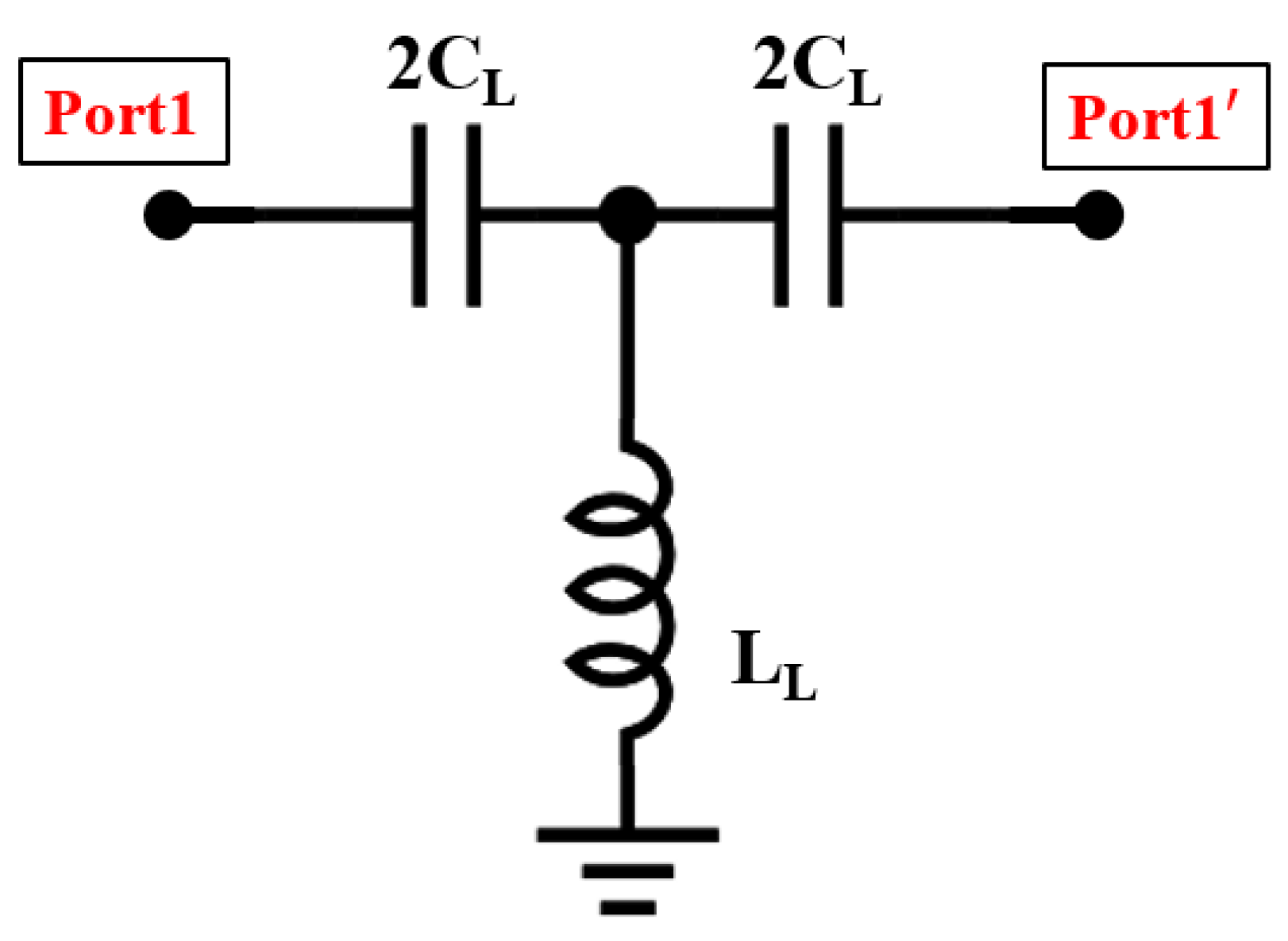
The left-handed (LH) characteristic of this structure dominates the phase and amplitude responses. The left-handed transmission line is first considered. Considering that the area required to implement inductors in 90 nm CMOS technology provided by TSMC is much larger than that for capacitors, we decided to use a T-model symmetric structure in the implementation of the unit cell for the left-handed transmission line, where the series capacitors are cascaded with parallel inductors and then cascaded with series capacitors, shown in
Figure 2.
The characteristic impedance and S
21 of this structure can be calculated using the ABCD Matrix from the T-model.
In order to create a 1/4-wavelength transmission line with an impedance of
= 70.7 Ω that can be used in the frequency band, it is necessary to calculate the required capacitance and inductance values to obtain the required minimum order. The phase of the left-hand transmission line can be derived using the ABCD Matrix from the T-model and transformation to an S-parameter and can be written as [
28]
Here, represents the phase of the transmission line, N denotes the order of the T-model, indicates the shunt inductance, and represents the series capacitance. From Equation (3), it can be observed that to minimize the area, only one unit cell (N = 1) is needed to achieve a +90° phase shift at the center frequency . In this case, the value inside the arctan function should approach infinity, which means .
Then
and the cutoff frequency of the unit cell in
Figure 2 is written as
The cutoff frequency is calculated to be 27.6 GHz for a center frequency of 39 GHz in this design. Additionally, as the number of stages increases, for instance, when N = 2 as described in Equation (3), the cutoff frequency decreases to 15 GHz, which indicates a broader operating bandwidth. However, this also results in an increased number of components, leading to a larger area. Therefore, N = 1 offers a satisfactory bandwidth, making it suitable for the design and enabling the construction of a compact structure.
The values of inductance and capacitance required for a pure left-handed transmission line composed of only one T-model can be calculated by solving the simultaneous equations in Equations (1) and (3). For a desired phase requirement of +90° at a center frequency of 39 GHz and a characteristic impedance of 70.7 Ω, the following values can be obtained.
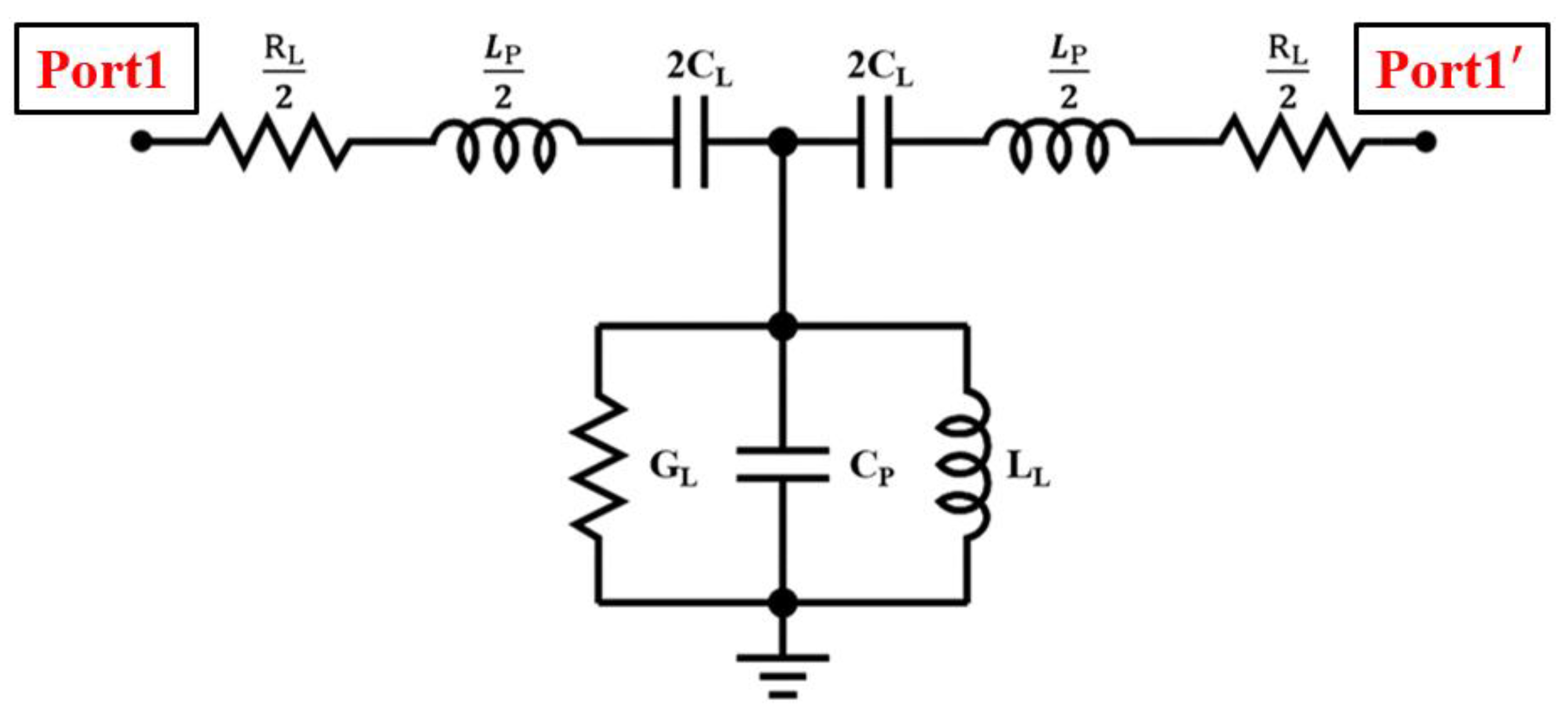
The created left-handed transmission line possesses the parasitic characteristics of the right-handed transmission line, causing a reduction in phase lead. Therefore, a composite left-handed and right-handed transmission line is proposed in the actual design.
It is crucial to consider the parasitic elements in a 1/4-wavelength CRLH transmission line,
and
. Thus, the actual equivalent circuit model can be represented as shown in
Figure 3. The values of
and
are highly dependent on the layout of the circuit.
arises from the inductance caused by the interconnecting lines between passive components, while
is due to the capacitance between all components and the ground plane,
is metal loss, and
is substrate loss.
The parasitic inductance and capacitance are generally very small, so the resulting phase can be simplified as
[
28]. And the actual phase of the left-handed transmission line is
In Equation (7), and represent the parasitic inductance capacitance, respectively. The parasitic right-handed circuits would cause a reduction in the leading phase magnitude formed by the left-handed line. The values of inductance and capacitance of the left-handed transmission line need to be reduced to maintain the desired +90° phase at the center frequency. Utilizing these parasitic right-hand circuits appears to reduce the capacitance and inductance values required for the left-hand transmission line. According to Equation (5), if the capacitance and inductance required for the left-hand transmission line are reduced, the cutoff frequency of the circuit is increased, and the increase in the cutoff frequency leads to a reduction in bandwidth. Although the circuit area is decreased, an increase in cutoff frequency results in a reduction in bandwidth.
The final fine-tuned values obtained from this process are
= 260 pH,
= 0.025 pF,
= 88 pH,
= 5.5 fF,
= 7.6 Ω, and
= 700 Ω. The full-wave simulation model is shown in
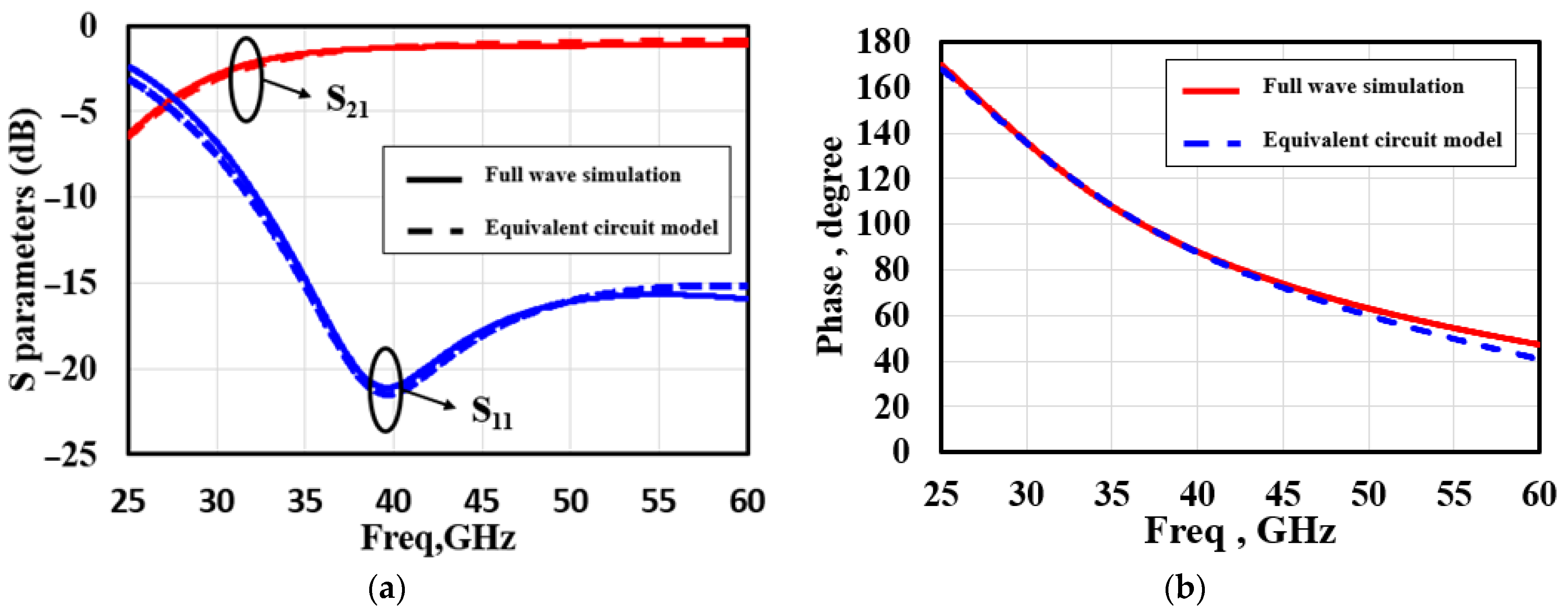
Figure 4, while the extracted values agree well with the results of the 3D full-wave simulation, as shown in
Figure 5a,b. Moreover, the phase is close to +90° at the center frequency of 39 GHz. The equivalent μ and ϵ of the left-handed quarter-wavelength transmission line can be calculated through the formula [
29].
As shown in
Figure 6, it can be seen that
and
are −40 and −15 at 39 GHz, respectively. The negative values confirm that the structure under consideration is a left-handed transmission line. Furthermore, these values are considerably higher than the
(≅3.8) of the CMOS process, resulting in a substantial reduction in the effective wavelength
[
30]. Additionally,
and
are both close to zero, indicating a low-loss structure. Compared to a traditional transmission line, the length of the CRLH transmission line is significantly shortened to 80 μm, which is about 8% of the length of a conventional transmission line.
2.2. Right-Handed Transmission Line Design
When designing the transmission line for the right-handed (RH) component, the parasitic circuit of each stage follows the same form as the inherent right-handed transmission line, consisting of series inductors and parallel capacitors. Therefore, there is no need to restrict the design to a single stage. Multi-stage transmission lines have very small capacitance and inductance values. Therefore, the calculated cutoff frequency will be much higher than the center frequency. Thus, the phase calculation formula can be simplified as [
28]
represents the phase of the transmission line, N2 represents the order of the right-handed transmission line model, represents the series inductance, and represents the shunt capacitance.
The right-handed slow-wave transmission line is achieved through a series of multi-order inductors and parallel capacitors, as shown in
Figure 7a. In order to consider a circuit with a compact size and symmetry, this periodic structure is connected by a transmission line (
), allowing it to be folded and thus reducing the overall space required. This structure can be simplified as two right-handed structures (RH1 and RH2) connected together; each structure is formed by 11 series of serial inductors and parallel capacitors, as shown in
Figure 7b. The values of the extracted inductance and capacitance are
= 21.5 pH and
= 4.45 fF, respectively. The resistance
is 0.2 Ω, and the conductance
is 6000 Ω.
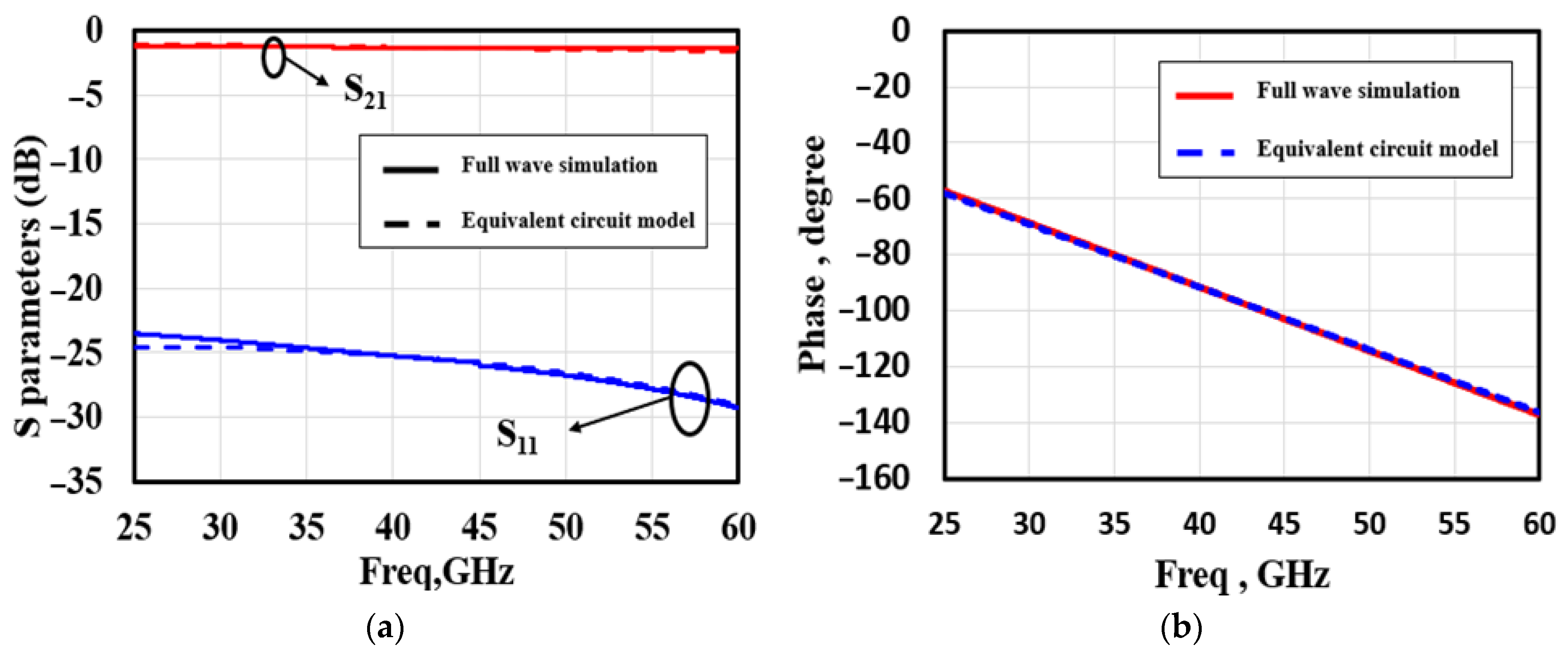
The comparison between the S-parameters and the phase of the extracted equivalent circuit and the full-wave simulation is shown in
Figure 8a,b. A good agreement is obtained, and the phase is close to −90° at the center frequency of 39 GHz.
Similarly, the equivalent μ and ε of the right-handed slow-wave transmission line can be calculated by Equations (8) and (9), as shown in
Figure 9.
and
are approximately 18 and 8, respectively. The positive values indicate that this transmission line possesses the right-handed characteristic, and the values are much larger than the substrate permittivity
= 12.9, ensuring that the group velocity of this structure is significantly less than the speed of light in free space and thus demonstrating a good slow-wave effect. Additionally,
and
are 1.5 and 0.5, respectively, indicating a low-loss structure. Furthermore, the length of this transmission line is only about 30% of the traditional transmission line.
2.3. Left-Handed and Right-Handed Rat-Race Coupler
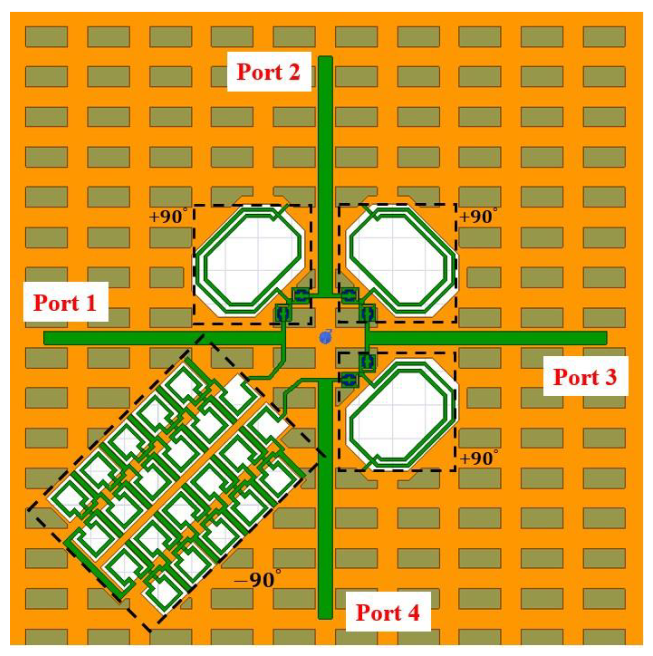
By combining the three designed CRLHs (+90°) and one right-handed slow-wave transmission line (−90°) shown in
Figure 10, the left-handed and right-handed rat-race coupler is proposed. The ground is constructed using two bottom metal layers in an alternating slot pattern to comply with the metal density rule of TSMC CMOS 90 nm technology.
For traditional rat-race couplers, the frequency-dependent phase difference between the differential outputs can be expressed as
. In the design of the left-handed and right-handed rat-race coupler, the phase difference is given by
It can be observed that
in the proposed CRLH coupler exhibits a parabolical frequency response compared to the traditional structure with linear response shown in
Figure 11, indicating that the operating bandwidth of the presented structure is significantly extended.
3. Implementation and Measurement Results
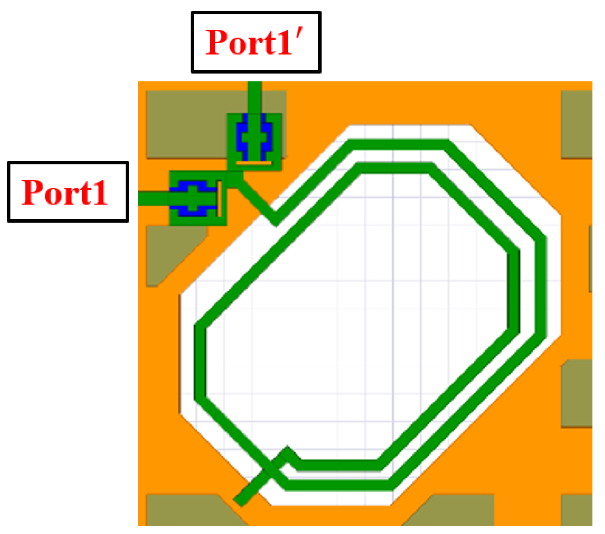
To validate the usefulness of the CRLH structure design, the miniaturized rat-race coupler is implemented by using a 90 nm CMOS process at a center frequency of 39 GHz to achieve good matching, phase balance, and low-loss imbalance over a wide bandwidth. The CRLH transmission line is created as a one-stage T-model structure with a Metal–Insulator–Metal (MIM) capacitor and a coiled inductor without underlying metal ground.
For the right-handed slow-wave transmission line design, a multi-stage slow-wave structure is created by combining the square-shaped inductors with short stub structures that provide sufficient capacitance. This arrangement enables a compact arrangement of periodic patterns, thereby reducing the overall layout area of the transmission line. In order to reduce the overall area more effectively, it is designed as a bent slow-wave transmission line. The chip photo of the four-port rat-race coupler is depicted in
Figure 12, featuring a core circuit area of 200 μm × 300 μm.
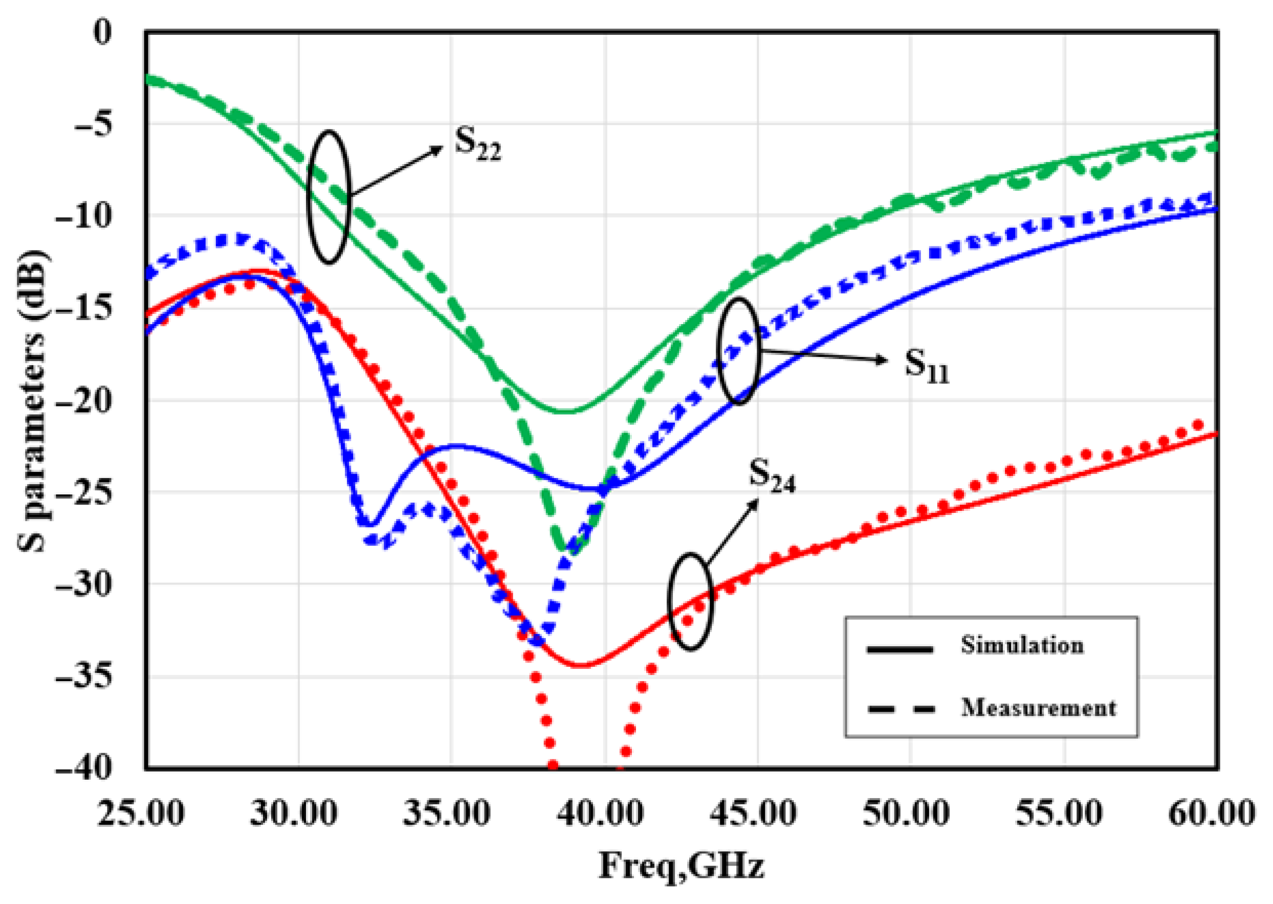
Figure 13 shows the measurement results of return loss and isolation. Since the proposed rat-race coupler is symmetrical in design, the return losses for port 1 and port 4 are the same, and the return losses for port 2 and port 3 are the same, so only the return losses of port 1 and port 2 are shown in
Figure 13. By analyzing the return loss measurement results, it can be seen that
and
are both less than −15 dB in the frequency range from 35 GHz to 43 GHz.
represents the isolation of the proposed rat-race coupler; it can be seen from
Figure 13 that the isolation is greater than 25 dB in the frequency range from 35 GHz to 43 GHz.
The proposed rat-race coupler can be used in two modes: differential mode and common mode, so
Figure 14 shows the insertion loss of the two modes. Port 1 is the differential mode input, and port 2 and port 4 are the differential mode output, so
and
represent the insertion loss of the differential mode. Port 3 is the common mode input, and port 2 and port 4 are the common mode output, so
and
represent the common mode insertion loss. Since the proposed rat-race coupler is symmetrical in design,
and
are the same, so
Figure 14 only shows three curves
,
, and
. In
Figure 14, the insertion loss of the three curves
,
, and
at 39 GHz is about 4.4 dB, and the loss variation is within 1 dB in the frequency range of 36 GHz to 48 GHz.
Figure 15 shows the phase difference for the differential port and common port, with targets of 180° and 0°, respectively. In the frequency range of 32 GHz to 60 GHz, the differential port phase error is maintained within the range of plus or minus 5° of 180°. In the frequency range of 34 GHz to 60 GHz, the common port phase error is maintained within the range of plus or minus 5° of 0°.
Table 1 shows the performance comparison of the proposed CRLH rat-race coupler with other millimeter-wave rat-race coupler designs. The data in the table are differential mode measurement results.
To make a consistent comparison of different designs, the calculation of fractional bandwidth follows some conditions under phase error < 5 degrees, return loss > 15 dB, and amplitude error < 1 dB. In addition to the comparison of electrical characteristics, the usage area is also a very important indicator. Moreover, to make the area comparison fair, the chip area is divided by the wavelength of the central operating frequency. Therefore, by analyzing these two parameters, it can be concluded that the proposed CRLH rat-race coupler possesses the optimal performance.
Since the amplitude error in [
21,
23] is greater than 1dB, and the return loss in [
25] is <15 dB, these three designs do not have fractional bandwidth. By comparing the fractional bandwidths, the proposed CRLH rat-race coupler has the widest bandwidth. In addition to the comparison of electrical characteristics, the size of the core circuit is also a very important indicator. To make the size comparison fair, the size of the core circuit is divided by the wavelength of the central frequency. It can be seen from
Table 1 that the proposed CRLH rat-race coupler has the second smallest area, second only to [
23], but the amplitude error of [
23] is also the largest in the comparison table. Therefore, considering the two factors of fractional bandwidth and chip area, the proposed CRLH rat-race coupler has the best performance.


