
Research on Two Improved High–Voltage–Transfer–Ratio Space–Vector Pulse–Width–Modulation Strategies Applied to Five–Phase Inverter
School of Electrical Engineering, Naval University of Engineering, Wuhan 430033, China
*
Author to whom correspondence should be addressed.
Electronics 2024, 13(8), 1546; https://doi.org/10.3390/electronics13081546
Submission received: 27 March 2024
/
Revised: 7 April 2024
/
Accepted: 10 April 2024
/
Published: 18 April 2024
Abstract
:Considering that the defects of traditional nearest–two–vector SVPWM (NTV–SVPWM) have a low voltage transfer ratio (VTR) and those of nearest–four–vector SVPWM (NFV–SVPWM) have a high output current harmonic, two improved space–voltage pulse–width–modulation (SVPWM) strategies are proposed in this paper, based on analyzing the harmonic characteristics of traditional NTV–SVPWM and NFV–SVPWM. The first strategy is to synthesize the referenced voltage vector according to the different weight factors by NTV–SVPWM and NFV–SVPWM. The second strategy is to synthesize the referenced voltage vector according to the different weight factors of NFV–SVPWM and the large vector. Compared to NTV–SVPWM, the simulation results show that the two proposed SVPWM strategies have lower output voltage errors and THDs. Compared to NFV–SVPWM, the simulation results show that the two proposed SVPWM strategies have higher VTRs and THDs. Compared to the two proposed SVPWM strategies, proposed SVPWM strategy one has a lower output voltage error and THD. The experimental results verify that the proposed modulation strategy is correct and feasible.
1. Introduction
The multiphase motor drive system has a lower torque ripple and fault tolerance performance, which is more suitable for occasions with high accuracy and reliability [1,2,3,4,5]. And its low–voltage and high–power characteristics can avoid voltage and current sharing problems caused by series and parallel power devices in three–phase power circuits [6,7]. Higher phase numbers enable it to have more control degrees of freedom. The fundamental and harmonic components can be decoupled through a space vector converter. The harmonic component can be controlled through the harmonic sub–plane, which can further improve the control characteristics of multiphase motors [8,9,10,11]. In multiphase voltage source inverter drive systems, the traditional NFV–SVPWM strategy has a lower output voltage THD, but its maximum VTR in the linear region is 0.812. The maximum VTR in the linear region based on the NTV–SVPWM strategy is 0.9512, but its output voltage THD is high. Therefore, the NFV–SVPWM strategy is widely used in the five–phase inverters.
In order to improve the load capacity and operational performance of the five–phase variable–frequency speed regulation system, many experts and scholars have conducted research on its modulation strategy, fault tolerant control, etc. [12,13,14,15,16,17,18,19,20,21,22,23,24]. The literature proposes a nearby space–vector fault–tolerant combination strategy for driver open–circuit faults, which achieves smooth operation of the motor [12]. In order to improve the utilization ratio of DC bus voltage, an improved NFV–SVPWM is proposed in [13]. According to different coefficients, the entire modulation range is divided into sinusoidal and non–sinusoidal modulation regions, which improves the voltage transmission ratio. A non–sinusoidal random SVPWM algorithm based on random switching delay and random vector assignment is proposed in [14], which can achieve the goal of harmonic dispersion by reducing the amplitude of higher harmonics without affecting the fundamental and third–harmonic outputs. A continuous SVPWM strategy for a class of five–phase inverters is proposed by rationally using zero vectors in [15], its switching times are 1/5 less than that of continuous space vector modulation, and the output voltage harmonic performance is better than that of the minimum–switching–loss SVPWM strategy. An NFV–SVPWM strategy that can suppress third harmonics is proposed in [16,17,18]. Three–phase–inverter over–modulation strategies are applied to multiphase inverters in [19,20,21,22]. A three–phase–inverter carrier over–modulation strategy is applied to the five–phase inverter over–modulation strategy, which increases the VTR of the five–phase inverter by 17% in the linear region [22,23,24]. In conclusion, to improve the VTR of the five–phase inverters, traditional three–phase inverter over–modulation strategies are mostly used in five–phase inverters. However, few studies directly and simultaneously investigate the SVPWM strategy of five–phase inverters to improve its VTR and optimize its harmonic characteristics.
In this paper, two improved SVPWM strategies applied to the five–phase inverter are proposed. Firstly, the basic structure of the five–phase inverter and the principle of the NTV–SVPWM and NFV–SVPWM strategies are introduced. Secondly, the harmonic characteristics of the output voltage with the NTV–SVPWM and NFV–SVPWM are analyzed. Thirdly, two improved SVPWM strategies based on different vector weighting designs are proposed and their harmonic characteristics are analyzed. Then, simulation and experiments are carried out on semi– and real platforms. Whereas the first two parts are the basis of this paper and are research that is currently more mature at present, this part proposes an improved strategy based on over–modulation, that is, a vector–weighted improvement. This paper is summarized in the final section.
2. Topological Structure and Space Voltage Vector Operating Principle of Five–Phase Inverter
2.1. Main Circuit Topology and Basic Modulation Modulation Strategy
Figure 1 shows the main circuit topology of a five–phase inverter system, consisting of a DC power supply, a five–phase inverter, and a five–phase R–L load.
Among them, this paper focuses on the further study of the space vector modulation strategy for five–phase inverters. Space–Vector Pulse–Width–Modulation (SVPWM) is a modulation technique commonly used in power electronics for controlling AC motor drives, inverters, and other systems. It is an improvement on the conventional PWM technique, providing higher power conversion efficiency and lower harmonic distortion. In SVPWM, a voltage or current signal is converted into a space vector, and then the output waveform is controlled by adjusting the amplitude and phase of the space vector. By choosing the combination of space vectors appropriately, precise control of the output waveform can be achieved, allowing the system to control total harmonic distortion (THD) within reasonable limits and to utilize the power capability of the power converter more efficiently. SVPWM is typically used to control a three–phase inverter, which is used to convert direct–current (DC) power to alternating–current (AC) power to drive an AC motor or to connect DC power to an AC power grid. By precisely regulating the pulse width and phase of the inverter output, SVPWM enables efficient power conversion and can provide stable output voltages and currents under different operating conditions. In conclusion, SVPWM technology has important applications in the field of power electronics in improving system performance and efficiency, and it is widely used in AC motor drives, power converters, and other power electronic devices.
2.2. Operating Principle of Five–Phase SVPWM
Let the switching function of the five–phase inverter be S = [Sa, Sb, Sc, Sd, Se]; then, the upper switch of the bridge arm of phase a of the inverter is on, and the lower switch is off; if Sa = 0, it is the opposite, and the other switching functions are similar. The output voltage of each phase of the inverter can be expressed as Ua = SaUD; Ub = SbUD; Uc = ScUD; Ud = SdUD; and Ue = SeUD, respectively. Therefore, the voltage space vector of the five–phase synchronous motor can be defined as
According to the above definition, a total of 32 voltage vectors can be calculated, and their spatial distribution is shown in Figure 2a. These vectors are divided into 4 groups, of which 10 are large, medium, and small vectors, forming three positive 10–sided shapes with different side lengths, and there are also two zero–vectors. The five–bit binary corresponding to each voltage vector in the figure is the switching function of that vector, indicating the operating state of the inverter at this time; the subscript of the voltage vector indicates the decimal number corresponding to the binary number.
Further study of the switching states corresponding to each vector reveals that the three effective vectors of large, medium, and small amplitudes correspond to the three operating states of the five–phase inverter, i.e., the 2/3 operation mode, the 1/4 operation mode, and the pseudo–2/3 operation mode, respectively. The so–called 2/3 mode of operation means that at a certain instant, the upper bridge arm of the inverter has two phases on and the lower bridge arm has three phases on or vice versa, and the phases that the upper bridge arm (or the lower bridge arm) is on are adjacent to each other, which results in the largest synthesized voltage vector and corresponds to a motor with a larger stator flux. The 1/4 mode of operation is similar to the 2/3 mode of operation, except that the resulting voltage vector is smaller. The difference between the pseudo–2/3 mode and the 2/3 mode is that the three phases of the upper or lower bridge arms that conduct at the same time are not all adjacent to each other, and there is a non–conducting phase inserted in the middle, which will result in an inconsistent direction of voltage vectors or stator fluxes that cancel each other out, and therefore should be avoided [15].
Figure 2 shows a vector block diagram of a five–phase inverter. The five–phase inverter has a total of 32 vectors, including 10 large vectors, 10 medium vectors, 10 small vectors, and 2 zero vectors, as shown in Table 1. The amplitudes of large, medium, and small vectors are as follows:
2.2.1. Nearest–Two–Vector SVPWM (NTV–SVPWM)
The strategy is the same as the traditional three–phase–inverter space voltage vector synthesis principle: first, determine the row sector k, and then synthesize the referenced voltage vector Uref with the two largest adjacent vectors. Assuming that the referenced voltage vector Uref is located in sector k, only the large vectors ULK and ULK+1 on both sides of sector k and the two zero–vectors U0 and U31 are used for vector synthesis, as shown in Figure 3. Assuming that the duration of the action of Uref is one switching cycle Ts, within one Ts, the duration of the action of ULK and ULK+1 is TLK and TLK+1, respectively. According to the volt–second balance principle, Equation (3) can be obtained.
The remaining time T0 = Ts − TLK − TLK+1 is supplemented by averaging the zero vectors U0 and U31.
Equation (4) can be obtained by solving Equation (3) in α–β coordinates as follows.
Equation (5) can be obtained by solving Equation (4):
The modulation ratio M is defined as the ratio of the amplitude of the referenced voltage vector Uref to the amplitude of the large vector UL, which is equal to the VTR.
In the linear modulation region, when TLK + TLK+1 = Ts, that is, the zero–vector action time is 0, the VTR of the NTV–SVPWM strategy can be calculated as 0.9512.
2.2.2. Nearest–Two–Vector SVPWM (NTV–SVPWM)
Assuming that Uref is located in sector k, vector synthesis can be performed using the large vectors ULK and ULK+1 corresponding to both sides of sector k, the middle vectors UMK and UMK+1, and the two zero–vectors U0 and U31, as shown in Figure 4.
The duration of the action of Uref is still one switching cycle Ts of the inverter. Within one Ts, the large vectors ULK and ULK+1 and the middle vectors UMK and UMK+1 are, respectively, TLK, TLK+1, TMK, and TMK+1. The remaining time T0 = Ts − TMK − TMK+1 − TLK − TLK+1 is supplemented by zero vectors U0 and U31.
According to the volt–second balance principle, Equation (7) can be obtained as follows:
Equation (8) can be obtained by solving Equation (7) in α–β coordinates.
From Equation (8), it can be seen that there are fewer equations than unknowns. According to linear algebra theory, there is no unique solution to the equation. Here, a constraint condition is added to make the action times TLK and TLK+1 of the large vector be x times the action times TMK and TMK+1 of the medium vector, which is expressed as Equation (9) and can be substituted to solve a specific basic solution system.
At the same time, in order to simplify the expression of the action time of each vector obtained by the solution, the amplitude ratio of the large vector to the medium vector is defined as . The action time of each vector can be obtained as shown in Equation (10).
In the linear modulation region, the VTR of the NFV–SVPWM strategy can be calculated as 0.812.
3. Harmonic Characteristics of Output Voltage of Traditional Space Voltage Vector Modulation
3.1. NTV–SVPWM
According to the volt–second balance principle, the referenced voltage vector is composed of adjacent voltage vectors, and its phase voltage in a sector can be represented by a duty cycle or action time, which is shown as follows:
In Equation (11), TLK and TLK+1 are the action times of the large vectors k and k + 1 (two vectors are adjacent), respectively. According to the space voltage vector synthesis principle, TLk and TLk+1 can be calculated as follows:
Substituting Equation (12) into Equation (13) yields
Using the same method for the remaining sectors, the expression of the A–phase output voltage within a fundamental cycle can be obtained as Equation (14).
According to Equation (14), the waveform of the A–phase output voltage within a fundamental cycle can be plotted, as shown in Figure 5.
The harmonic characteristics of the NTV–SVPWM strategy can be obtained by Fourier decomposition. The Fourier decomposition expression is shown as follows:
In Equation (15),
Since the A–phase reference wave is even–symmetric, its expression does not contain the bn term, and a0 = 0. The nth harmonic amplitude an is calculated as follows:
In Equation (16),
From above, the corresponding ratio between the amplitude of each harmonic and the amplitude of the fundamental wave can be calculated and plotted, as shown in Figure 6. From Figure 6, it can be seen that the reference wave obtained using the NTV–SVPWM strategy has poor quality and contains a large number of third and fifth harmonics.
3.2. NFV–SVPWM
Similarly, the referenced voltage expression with NFV–SVPWM can be calculated by referring to the two–vector harmonic characteristic analysis as follows:
Defining x as the ratio of a large vector to a medium vector in the same direction,
The nth harmonic amplitude an of the A–phase output voltage can be obtained as follows:
In Equation (19),
The numerical calculation shows that the value of x does not affect the fundamental wave amplitude a0 ≈ 0.470, and the nth harmonic amplitude is mainly determined by x. Harmonic distortion rate THD is defined as follows:
Considering that the THD is very low after the 40th order, the curve of THD varying with x is plotted through numerical simulation calculation, as shown in Figure 7. As can be seen from Figure 7, as x increases, the THD decreases first and then increases. When x = 1.618, which is the ratio of the amplitude of a large vector to a medium vector, the third harmonic is eliminated and the harmonic content is lowest. After that, as x increases, the output voltage THD continues to increase, indicating that the output voltage harmonics will increase with the increase in the ratio of the large vector to the referenced voltage vector.
4. Two Improved SVPWM Strategies Based on Multi–Vector Weighting
4.1. SVPWM Strategy One
4.1.1. Working Principle
The voltage transfer ratio described in this paper is also the ratio of the output voltage of the inverter to the input voltage, because the input voltage is usually certain, and the output voltage is positively correlated with the modulation ratio m. Thus, the enhancement in the voltage transfer ratio described in this paper can also be interpreted as an improvement in the modulation ratio, but in the process of modulation with the improvement in the modulation ratio, it is inevitable that the harmonic content will increase, so in the later experiments, we can see that indeed harmonics have increased. The harmonic content is found to increase, but the fundamental amplitude of the output voltage is improved; in this regard, the voltage transfer ratio is also improved to achieve the purpose of the experiment.
In order to improve the VTR and minimize the impact on output voltage harmonics, an improved SVPWM strategy based on the coordinating optimization and design of two–vectors and four–vectors is proposed, which combines four–vector Us4 and two–vector Us2 to synthesize a referenced voltage vector Uref. The amplitudes of four–vector Us4 and two–vector Us2 are as follows:
The referenced voltage vector Uref is composed of four–vector Us4 and two–vector Us2 and is calculated as follows:
where s and b are the weight factors of four–vector Us4 and two–vector Us2, respectively. From Equations (6), (21), and (22), in order to minimize output voltage errors and ensure that the fundamental amplitude of the output voltage is the desired output value according to M, the following equation exists:
According to the analysis in Sections III.A and III.B, in order to reduce the harmonic content of the output voltage as much as possible, the weight factor s of the four–vector Us4 should be as large as possible, and the weight factors s and b of the four–vector Us4 and the two–vector Us2 can be obtained as follows:
From Equations (22) and (24), when M = 0.812 and s = 1, it is NFV–SVPWM and the referenced voltage vector rotates between the large vector and the medium vector. When M = 0.9512 and s = 0, it is NTV–SVPWM and the referenced voltage vector rotates along the tangent circle of the large vector. Assuming that the referenced voltage vector is located in sector 1, the space voltage four–vector Us4 and two–vector Uh2 are synthesized from their corresponding vectors showing as follows, respectively.
The action time of Us4 and Us2 is calculated and obtained as follows.
The use of four–vectors and two–vectors to synthesize the reference voltage ensures that the space vector is always in the four–vector modulation mode, and to avoid the simultaneous turn–on or turn–off state of the switch tubes. Therefore, the modulation is a pseudo–over–modulation method, its modulation range is [0.812, 0.9512], and the minimum four–vector action time is set to its lower limit value based on the power device’s ON and OFF characteristics, to avoid the over–modulation strategy entering a separate two–vector modulation.
4.1.2. Harmonic Characteristics
According to the above analysis, the referenced voltage vector is composed of four–vectors and two–vectors according to a certain weight factor. According to the volt–second balance principle, reducing the four–vector action time and increasing the two–vector action time are equivalent to reducing the four–vector amplitude and increasing the two–vector amplitude within a switching cycle. The harmonic characteristics of the output voltage can be seen as adjusting the ratio of the large vector action time to the medium vector action time. From Equations (18) and (23), the ratio y of the action time of the large vector to the medium vector in the proposed modulation can be calculated as follows:
Referring to the four–vector harmonic characteristic analysis method, the THD of the output voltage under different s and x values is calculated through numerical simulation, as shown in Figure 8. As can be seen from Figure 8, when x is fixed, the THD decreases first and then increases with s, and it is basically concentrated in the ratio of the large vector to medium vector reaching the minimum value around 1.618. When s is fixed, the THD also decreases first and then increases, and the minimum value is also basically concentrated in the ratio of the large vector to medium vector near 1.618. The reason is that the third harmonic is the main harmonic, and when the third harmonic is suppressed, the THD of the output voltage is significantly reduced. According to Equation (22), in order to improve the VTR, appropriately increasing the ratio of the action time of the large vector to the medium vector can increase the fundamental amplitude of the output voltage, but increasing the action time of the large vector and the medium vector will inevitably increase the THD of the output voltage. Therefore, the proposed modulation strategy improves the fundamental amplitude of the output voltage at the cost of worsening the output voltage.
4.2. SVPWM Strategy Two
4.2.1. Working Principle
According to the analysis in Section IV.A, the use of a modulation strategy weighted by NFV–SVPWM and NTV–SVPWM has a relatively large computational complexity. To reduce the computational complexity, NFV–SVPWM and a single large vector are used to synthesize a referenced voltage vector; the referenced voltage vector Uref is composed of four–vector Us4 and a large vector ULK(ULK+1). The specific calculation is as follows:
s is redefined as shown in Equation (30):
Assuming that the referenced voltage vector Uref is located in sector 1, the space voltage four–vector Us4 and the large vector ULK(ULK+1) are synthesized from their corresponding vectors, respectively.
And then the action time of Us4 and the large vector ULK(ULK+1) are calculated and obtained as follows:
The other sectors can be calculated by referring to the above calculation.
4.2.2. Harmonic Characteristics
According to the principle of vector synthesis, the harmonic characteristics of the output voltage of the modulation method mentioned in this section are the superposition of the harmonic characteristics corresponding to the four–vector Us4 and the large vector ULK(ULK+1). The harmonic characteristics of the four–vector Us4 are analyzed in Section IV.A, and the harmonic characteristics of the output voltage of the large vector ULK(ULK+1) are discussed here. According to Equations (28), (30), and (31), the referenced voltage vector based on large vector synthesis is a square wave, and the harmonic characteristics of the square wave are shown in Equation (35).
It can be seen that compared to the four–vector Us4, the harmonic content of each order is higher when the referenced voltage vector is directly synthesized from a large vector, but the fundamental wave of the output voltage is also higher. Therefore, using this modulation can improve the VTR of the five–phase inverter, but due to the asymmetry of the vector action time, the THD of the output voltage will be higher.
5. Simulation Research and Experimental Verification
5.1. Simulation Results
A five–phase inverter with the R–L load simulation model is built based on Matlab/Simulink software. The simulation parameters are set as shown in Table 2.
Figure 9a,b show the amplitude of the fundamental wave of the output line voltage UAB and the THD of the output phase current iA of the five–phase inverter with M changing under proposed SVPWM strategies one and two, NTV–SVPWM and NFV–SVPWM, respectively.
From Figure 9a, it can be seen that the output voltage increases as M increases under proposed SVPWM strategies one and two, and NTV–SVPWM. Proposed SVPWM strategies one and two, and NTV–SVPWM can all accurately track the desired output voltage, and the error between proposed SVPWM strategy two and the desired voltage is slightly large. However, the output voltage of the NFV–SVPWM strategy remains basically unchanged as M increases, mainly because when M = 0.812, the operation time of the synthesized vectors UMK, UMK+1, ULK, and ULK+1 reaches the maximum effective value, that is to say, the zero–vector operation time is 0. Even if M increases, the operation time of each synthesized vector remains unchanged, making the output phase voltage unchanged as M increases.
As can be seen from Figure 9b, since the action time of the synthesis vector under the NFV–SVPWM strategy remains unchanged, the THD of its output phase current does not change. Although the output voltage of the NTV–SVPWM strategy increases with M, its THD does not change significantly. The main reason is that the action time of the synthesis vector changes proportionally, making the synthesized referenced voltage vector waveform unchanged. However, the two proposed SVPWM strategies change the ratio of the action time of the large vector to the medium vector, and as M increases, the action time of the large vector continues to increase, leading to the increase in the THD of the output current. The simulation results are consistent with the theoretical analysis. The simulation results show that the two proposed SVPWM strategies can effectively improve the fundamental amplitude of the output voltage of the five–phase inverter, and their THD is lower than that of NTV–SVPWM and higher than that of NFV–SVPWM.
Figure 10 shows the output phase voltage, phase current, and FFT spectrum under the four SVPWM strategies when M = 0.89. As shown in Figure 10, compared to NFV–SVPWM, the two proposed SVPWM strategies can effectively increase the fundamental amplitude of the output voltage, but the output current THD will increase quickly. Compared to the NTV–SVPWM, the output voltage continuously increases as M increases, but the output current with proposed SVPWM strategy one has a better sinusoidal waveform and lower THD. It can be seen that using the two proposed SVPWM strategies can effectively improve the fundamental amplitude of the output voltage and have better output performances.
5.2. Experimental Verification
In order to verify how correct the theoretical analysis and the feasibility of the proposed strategies is, both of the semi–physical and real experimental platforms composed of DSP + FPGA are built and shown as Figure 11, and the experimental results are almost the same. The experimental parameters are consistent with the simulation parameters.
Figure 12, Figure 13 and Figure 14 show the output current and harmonic distortion rate of the five–phase inverter under the four SVPWM strategies with M = 0.83, 0.89, and 0.951, respectively. As can be seen from the figure (under the same modulation strategy), with M increasing, the output current of traditional NFV–SVPWM remains unchanged, with the maximum M = 0.812. The output current of traditional NTV–SVPWM continuously increases, but its THD does not change too much, due to the same distribution of its output harmonic characteristics, which is independent of M. Therefore, it can be known that both the output voltage amplitude and output current THD increase with M, but proposed SVPWM one has better output characteristics than that of proposed SVPWM two.
From Figure 12, Figure 13 and Figure 14, compared to NFV–SVPWM, it can be seen that the output voltage of proposed SVPWM strategies one and two continuously increases as M increases; however, the THD of the output current also increases. The voltage output capabilities of traditional NTV–SVPWM and proposed SVPWM strategies one and two are identical, but the THD of the output current with proposed SVPWM strategies one and two is smaller than with traditional NTV–SVPWM. The experimental results are consistent with the theoretical analysis and simulation results, verifying that the theoretical analysis is correct and the proposed SVPWM strategies are feasible.
It is also easy to conclude from the previous validation section that there are also advantages and disadvantages of the two traditional modulation strategies and the two improved modulation strategies, which is expressed in Table 3 below.
6. Conclusions and Prospects
Considering the advantages of the high output voltage of NTV–SVPWM and the low THD of NFV–SVPWM, and attempting to best overcome the disadvantages of the high THD of NTV–SVPWM and the low output voltage of NFV–SVPWM, two improved SVPWM strategies are proposed by redesigning the weighting factors and vectorial combinations of Us4, Us2, and ULK(ULK+1) based on analyzing the output harmonic characteristics of NFV–SVPWM and NTV–SVPWM, where M improves from 0.812 to 0.951. The reference voltage vector Uref is synthesized by Us4 and Us2 with proposed SVPWM strategy one, and the referenced voltage vector Uref is synthesized by Us4 and ULK(ULK+1) with proposed SVPWM strategy two. Compared to NFV–SVPWM, the simulation results show that the two proposed SVPWM strategies have lower output voltage errors, but both of the THDs of the two proposed SVPWM strategies are higher. Compared to NTV–SVPWM, the simulation results show that the two proposed SVPWM strategies have lower output voltage errors and THDs. Compared to the two proposed SVPWM strategies, proposed SVPWM strategy one has a lower output voltage error and THD. Considering various factors comprehensively, proposed SVPWM strategy one is more suitable for five–phase inverters. The experimental results show that the two proposed SVPWM strategies are correct and feasible.
The two improvement methods proposed in this paper can improve the fundamental amplitude of the output voltage on the basis of over–modulation, but it itself carries the disadvantage of high harmonic content, for which relevant scholars can, according to the ideas provided in this paper, follow–up on the improvement in the external circuit based on the study of a new strategy to improve the fundamental amplitude of the output voltage, and they can reduce the harmonic content.
Author Contributions
Conceptualization, M.J.; methodology, Y.X.; software, B.Z.; validation, M.J., Y.X., and B.Z.; formal analysis, M.J.; investigation, B.Z.; resources, Y.X.; data curation, M.J.; writing—original draft preparation, M.J.; writing—review and editing, M.J.; visualization, Y.X.; supervision, B.Z.; project administration, Y.X.; funding acquisition, Y.X. All authors have read and agreed to the published version of the manuscript.
Funding
This research was funded by the National Natural Science Foundation of China (Grant Nos. 51877212).
Data Availability Statement
Data are contained within the article.
Conflicts of Interest
The authors declare no conflict of interest.
References
- Liu, G.; Song, C.; Chen, Q. FCS–MPC– based fault–tolerant control of five–phase IPMSM for MTPA operation. IEEE Trans. Power Electron. 2020, 35, 2882–2894. [Google Scholar] [CrossRef]
- Yu, B.; Song, W.; Guo, Y. A Simplified and Generalized SVPWM Scheme for Two–Level Multiphase Inverters with Common–Mode Voltage Reduction. IEEE Trans. Ind. Electron. 2022, 69, 1378–1388. [Google Scholar] [CrossRef]
- Barrero, F.; Bermudez, M.; Duran, M.J.; Salas, P.; Gonzalez–Prieto, I. Assessment of a Universal Reconfiguration–less Control Approach in Open–Phase Fault Operation for Multiphase Drives. Energies 2019, 12, 4698–4709. [Google Scholar] [CrossRef]
- Liu, G.; Song, C.; Xu, L.; Du, K. SVPWM–based fault–tolerant control strategy under two–phase open–circuit fault of five–phase permanent–magnet synchronous motor. Trans. China Electrotech. Soc. 2019, 34, 23–32. [Google Scholar]
- Tian, B.; Mirzaeva, G.; An, Q.T.; Sun, L.; Semenov, D. Fault–tolerant control of a five–phase permanent magnet synchronous motor for industry applications. IEEE Trans. Ind. Appl. 2018, 54, 3943–3952. [Google Scholar] [CrossRef]
- Liu, Z.; Li, Y.; Zheng, Z. Control and drive techniques for multiphase machines: A review. Trans. China Electrotech. Soc. 2017, 32, 17–29. [Google Scholar]
- Liu, Z.; Zheng, Z.; Li, Y. Enhancing fault–tolerant ability of a nine–phase induction motor drive system using fuzzy logic current controllers. IEEE Trans. Energy Convers. 2017, 32, 759–769. [Google Scholar] [CrossRef]
- Wang, Y.; Wang, Z. A novel spatial vector modulation strategy for multiphase three–level inverters based on vector space decoupling. Proc. CSEE 2018, 38, 3316–3324. [Google Scholar]
- Bermudez, M.; Gonzalez–Prieto, I.; Barrero, F.; Guzman, H.; Kestelyn, X.; Duran, M.J. An experimental assessment of open–phase fault–tolerant virtual–vector–based direct torque control in five–phase induction motor drives. IEEE Trans. Power Electron. 2018, 33, 2774–2784. [Google Scholar] [CrossRef]
- Zhou, C.; Yang, G.; Su, J.; Sun, G. Phase loss fault tolerance control strategy of dual three–phase permanent magnet synchronous motor based on normal decoupling transformation. Trans. China Electrotech. Soc. 2017, 32, 86–96. [Google Scholar]
- Qin, Y.; Zhu, H. Third harmonic injection type five–phase bearingless permanent magnet synchronous motor torque and suspension force performance optimization. Proc. CSEE 2018, 38, 6701–6711. [Google Scholar]
- Chen, C.; Chen, Z.; Zhao, J.; Gao, Z.; Liu, X.; Liao, X. A novel PMSM space vector fault tolerant combination stategy based on five–phase current source inverter. Trans. China Electrotech. Soc. 2020, 35, 404–412. [Google Scholar]
- Gao, H.; Yang, G.; Liu, J. Research of space vector PWM techniques for five–phase voltage source inverter. Proc. CSEE 2014, 6, 2917–2925. [Google Scholar]
- Zhu, L.; Bu, F.; Huang, W.; Pu, T. Non–sinusoidal dual random space vector pulse width modulation strategy for five–phase inverter. Trans. China Electrotech. Soc. 2018, 33, 4824–4833. [Google Scholar]
- Yu, F.; Zhang, X.; Li, H.; Song, Q. Space vector PWM control of five–phase inverter. Proc. CSEE 2005, 25, 40–46. [Google Scholar]
- Yu, F.; Zhang, X.; Li, H.; Xiang, D. Discontinuous space vector PWM control of five–phase inverter. Trans. China Electrotech. Soc. 2006, 21, 26–30. [Google Scholar]
- Bu, F.; Pu, T.; Liu, Q.; Ma, B.; Degano, M.; Gerada, C. Four–Degree–of–Freedom Overmodulation Strategy for Five–Phase Space Vector Pulsewidth Modulation. IEEE J. Emerg. Sel. Top. Power Electron. 2021, 9, 1578–1590. [Google Scholar] [CrossRef]
- Tawfiq, K.B.; Ibrahim, M.N.; Sergeant, P. An Enhanced Fault–Tolerant Control of a Five–Phase Synchronous Reluctance Motor Fed from a Three–to–Five–Phase Matrix Converter. IEEE J. Emerg. Sel. Top. Power Electron. 2022, 10, 4182–4194. [Google Scholar] [CrossRef]
- Wu, L.; Li, J.; Lu, Y.; He, K. Strategy of Synchronized SVPWM for Dual Three–Phase Machines in Full Modulation Range. IEEE Trans. Power Electron. 2022, 37, 3272–3282. [Google Scholar] [CrossRef]
- Zhu, Y.; Gu, W.; Lu, K.; Wu, Z. Vector Control of Asymmetric Dual Three–Phase PMSM in Full Modulation Range. IEEE Access 2020, 8, 104479–104493. [Google Scholar] [CrossRef]
- Priestley, M.; Fletcher, J.E. Space–vector PWM technique for five phase open–end winding PMSM drive operating in the overmodulation region. IEEE Trans. Ind. Electron. 2018, 65, 6816–6827. [Google Scholar] [CrossRef]
- Vancini, L.; Mengoni, M.; Rizzoli, G.; Sala, G.; Zarri, L.; Tani, A. Carrier–Based PWM Overmodulation Strategies for Five–Phase Inverters. IEEE Trans. Power Electron. 2021, 36, 6988–6999. [Google Scholar] [CrossRef]
- Gu, L.; Chen, Q.; Zhao, W.; Liu, G.; Xia, Y. Inter–phase short–circuit fault–tolerant control for five–phase permanent magnet fault–tolerant motors. Trans. China Electrotech. Soc. 2022, 37, 1972–1981. [Google Scholar]
- Chen, Q.; Gu, L.; Lin, Z.; Liu, G. Extension of space–vector–signal–injection based MTPA control into SVPWM fault–tolerant operation for five–phase IPMSM. IEEE Trans. Ind. Electron. 2020, 67, 7321–7333. [Google Scholar] [CrossRef]
Figure 1.
Main circuit of five–phase inverter system.
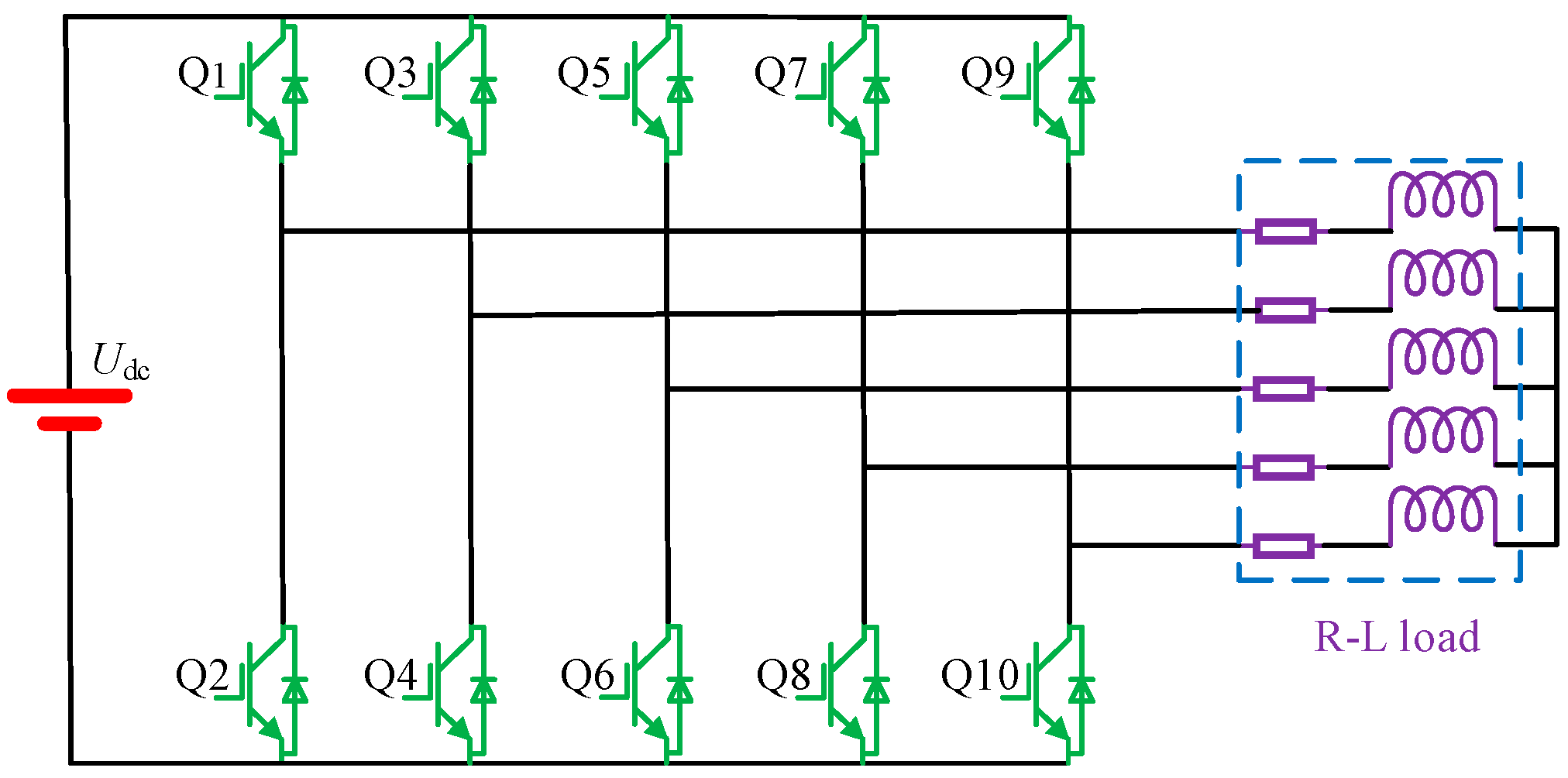
Figure 2.
Schematic diagram of space voltage vector and composite vector.


Figure 3.
Vector synthesis of NTV–SVPWM in sector k.

Figure 4.
Vector synthesis of NFV–SVPWM in sector k.
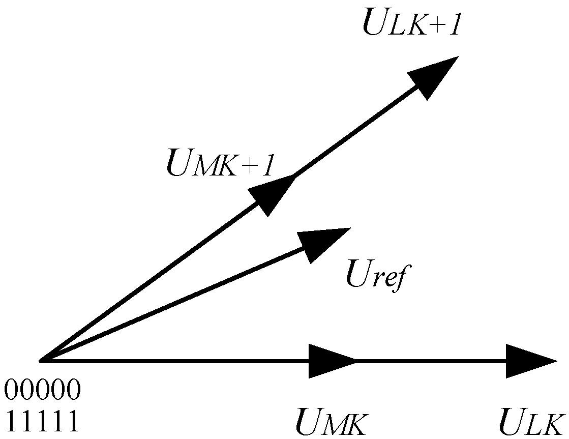
Figure 5.
A–phase referenced wave of NTV–SVPWM.

Figure 6.
Harmonic characteristics with NTV–SVPWM.
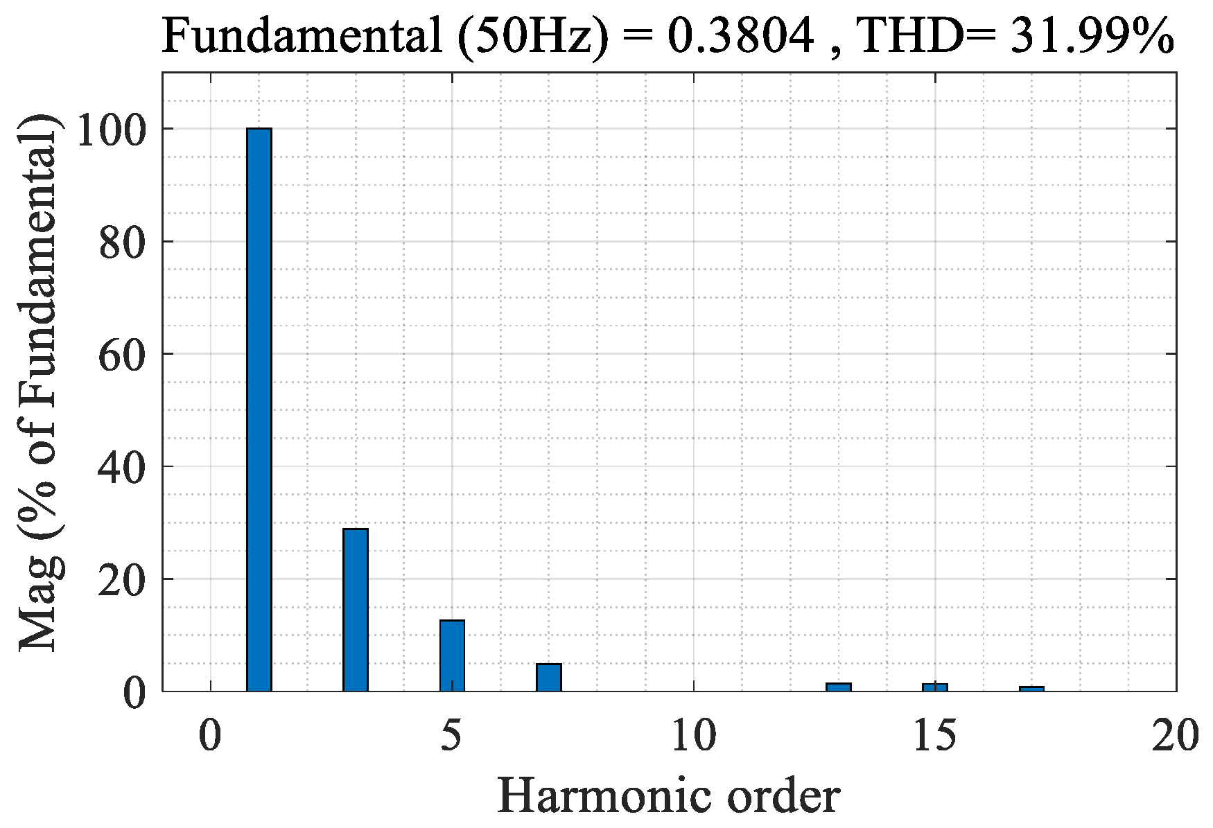
Figure 7.
THD of NFV–SVPWM varies with x.

Figure 8.
Output voltage THD varying with s and x.
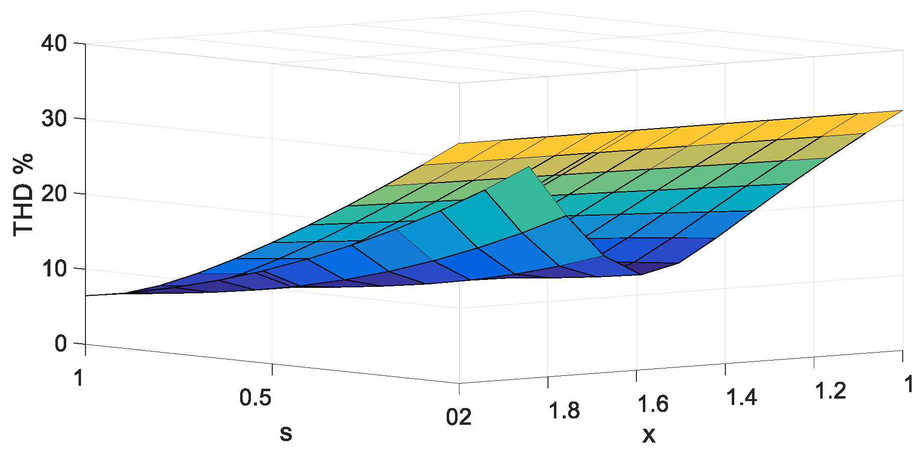
Figure 9.
Simulation results of output–phase–voltage fundamental wave amplitude and phase current THD varying with M under four SVPWM strategies.
Figure 9.
Simulation results of output–phase–voltage fundamental wave amplitude and phase current THD varying with M under four SVPWM strategies.
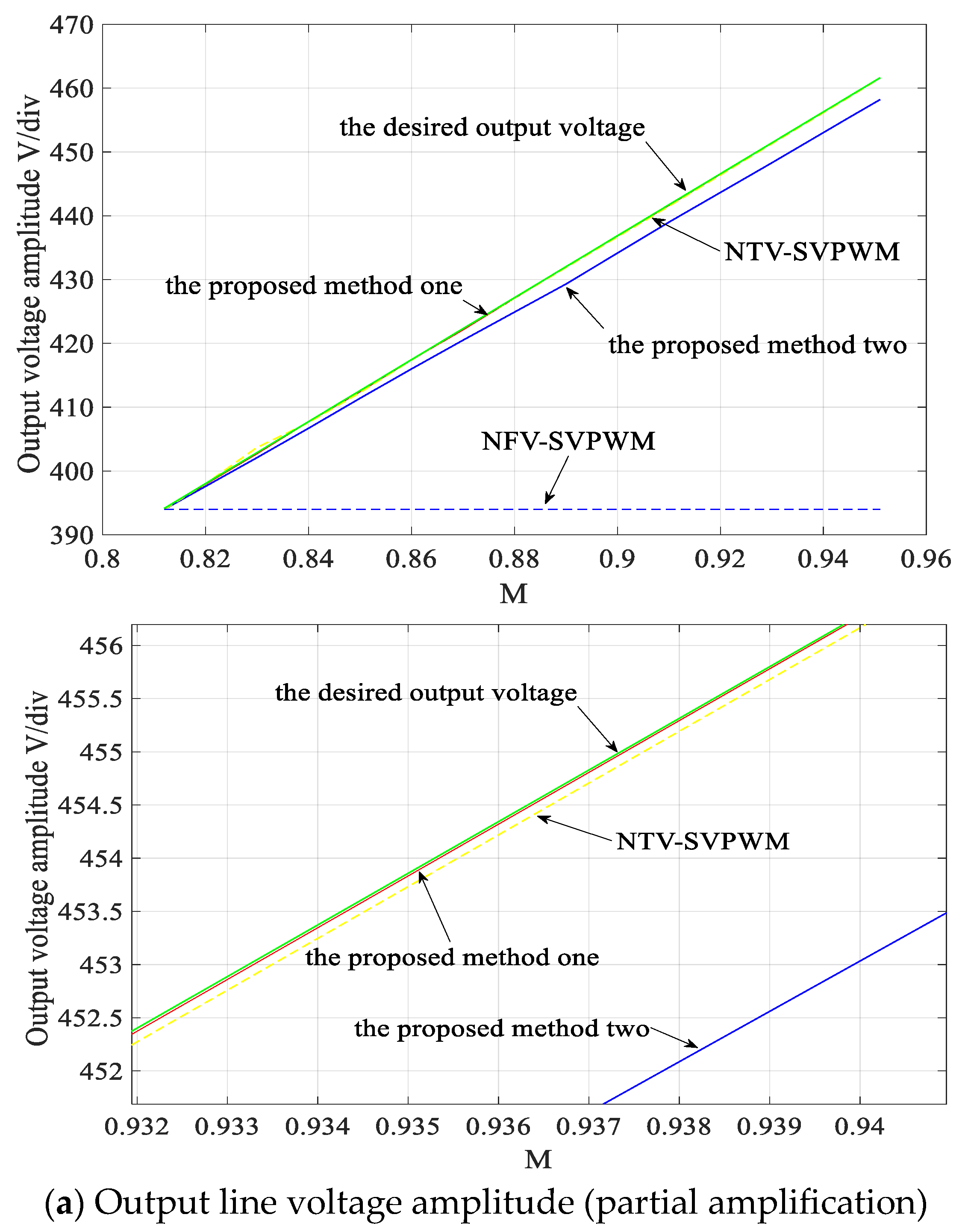
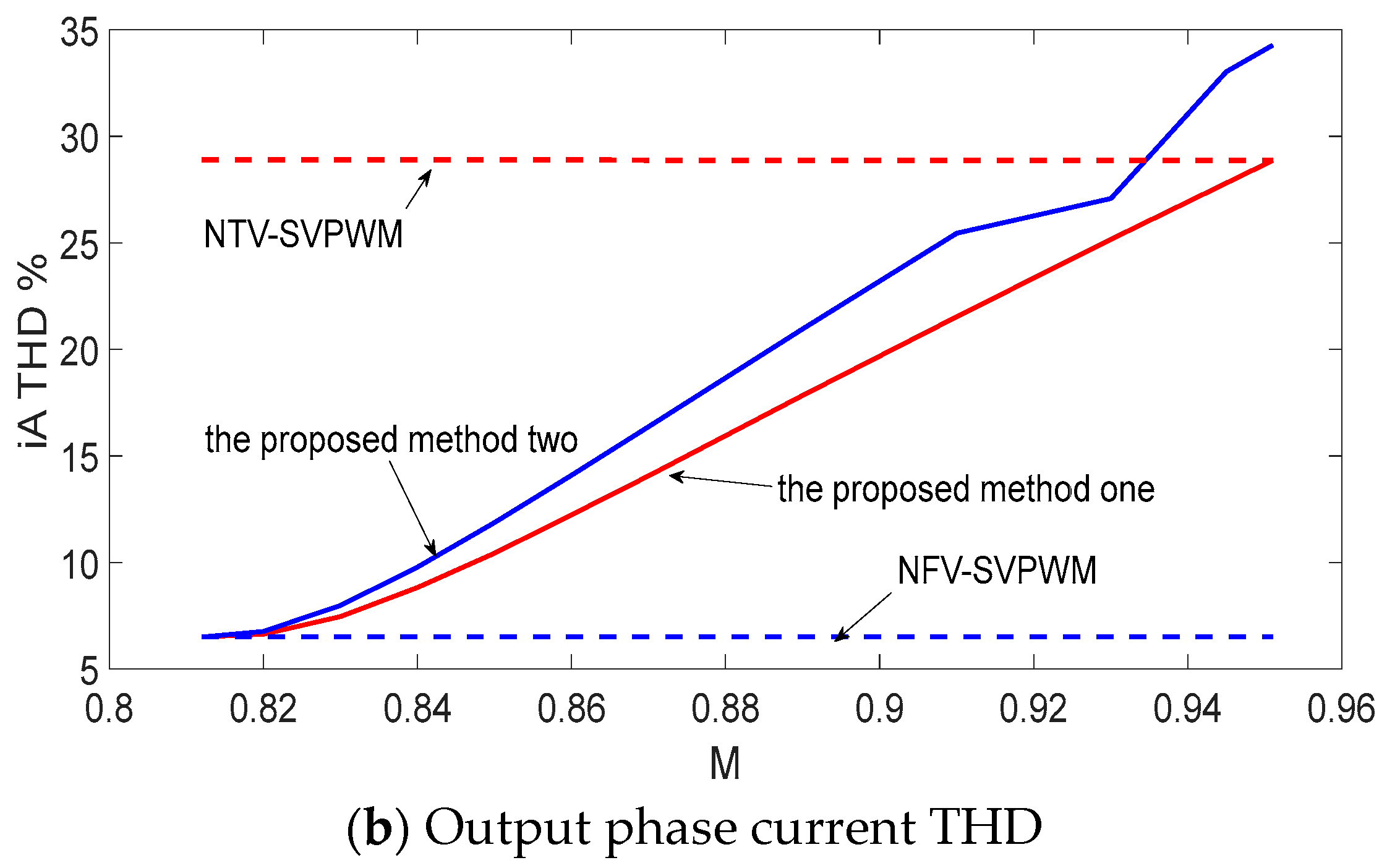
Figure 10.
Output phase voltage, phase current, and FFT spectrum under four SVPWM strategies when the modulation ratio is 0.89.
Figure 10.
Output phase voltage, phase current, and FFT spectrum under four SVPWM strategies when the modulation ratio is 0.89.

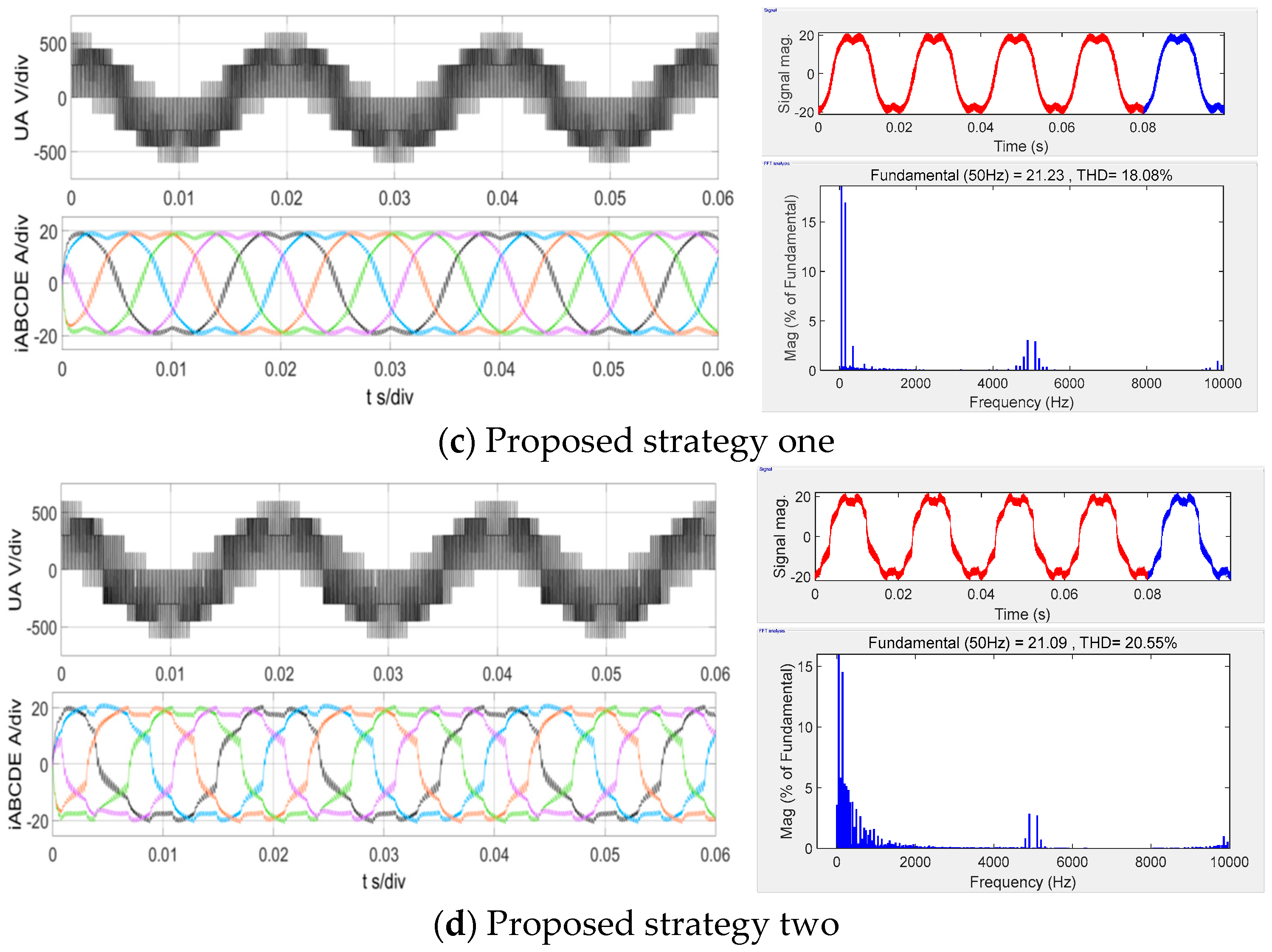
Figure 11.
Semi–and real physical experimental platforms.
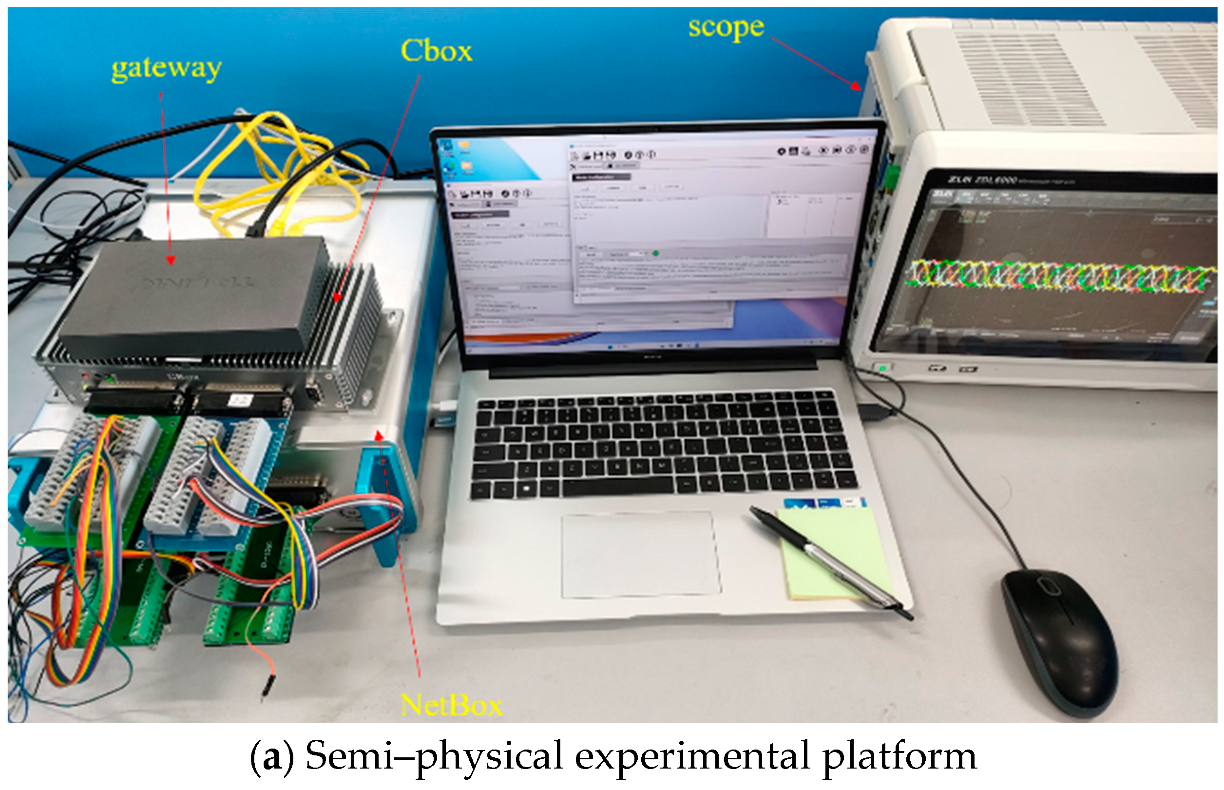

Figure 12.
Experimental results of output current and its THD with M = 0.83. (a) Traditional NFV–SVPWM. (b) Traditional NTV–SVPWM. (c) Proposed strategy one. (d) Proposed strategy two.
Figure 12.
Experimental results of output current and its THD with M = 0.83. (a) Traditional NFV–SVPWM. (b) Traditional NTV–SVPWM. (c) Proposed strategy one. (d) Proposed strategy two.
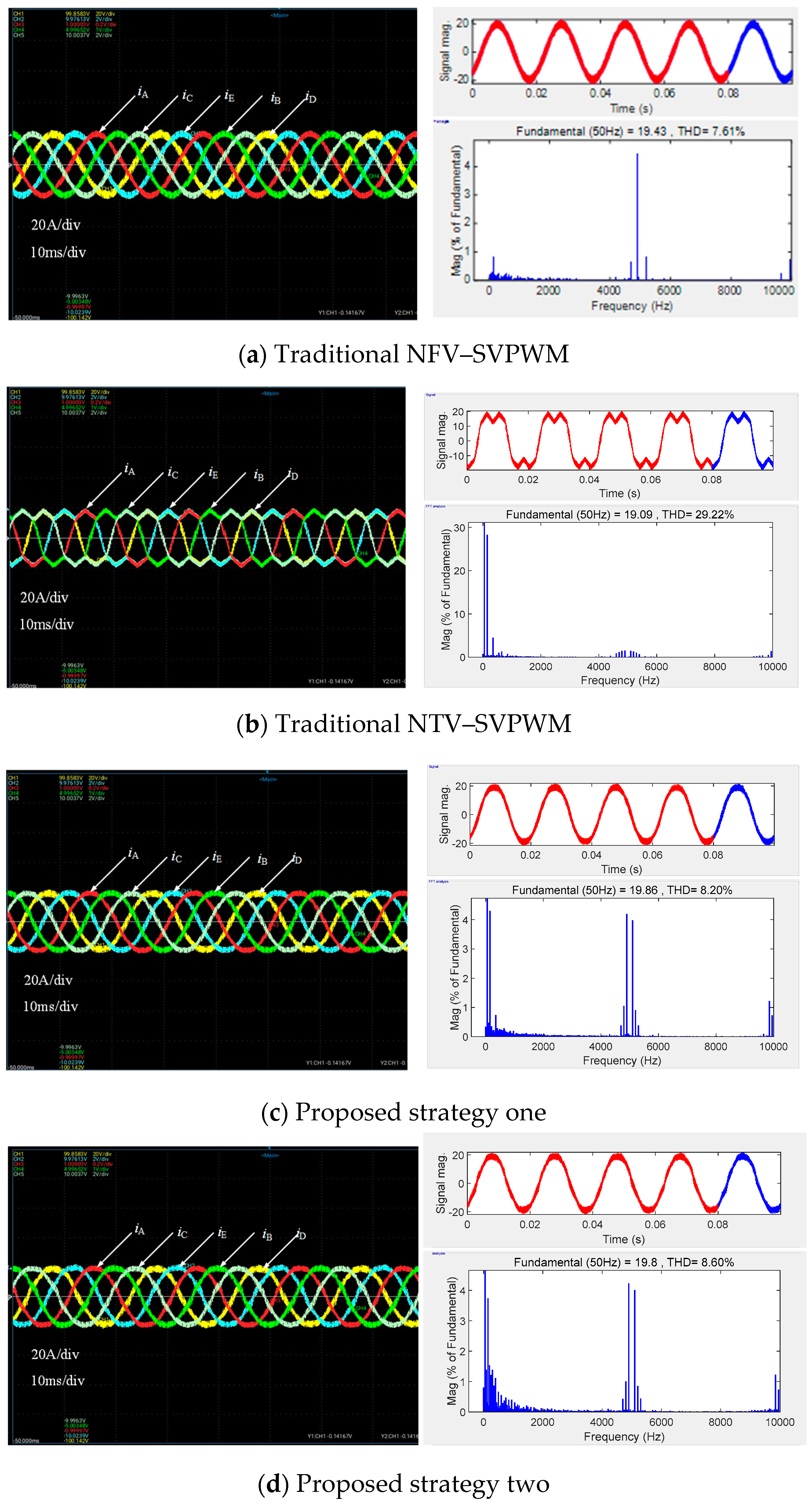
Figure 13.
Experimental results of output current and its THD with M = 0.89. (a) Traditional NFV–SVPWM. (b) Traditional NTV–SVPWM. (c) Proposed strategy one. (d) Proposed strategy two.
Figure 13.
Experimental results of output current and its THD with M = 0.89. (a) Traditional NFV–SVPWM. (b) Traditional NTV–SVPWM. (c) Proposed strategy one. (d) Proposed strategy two.
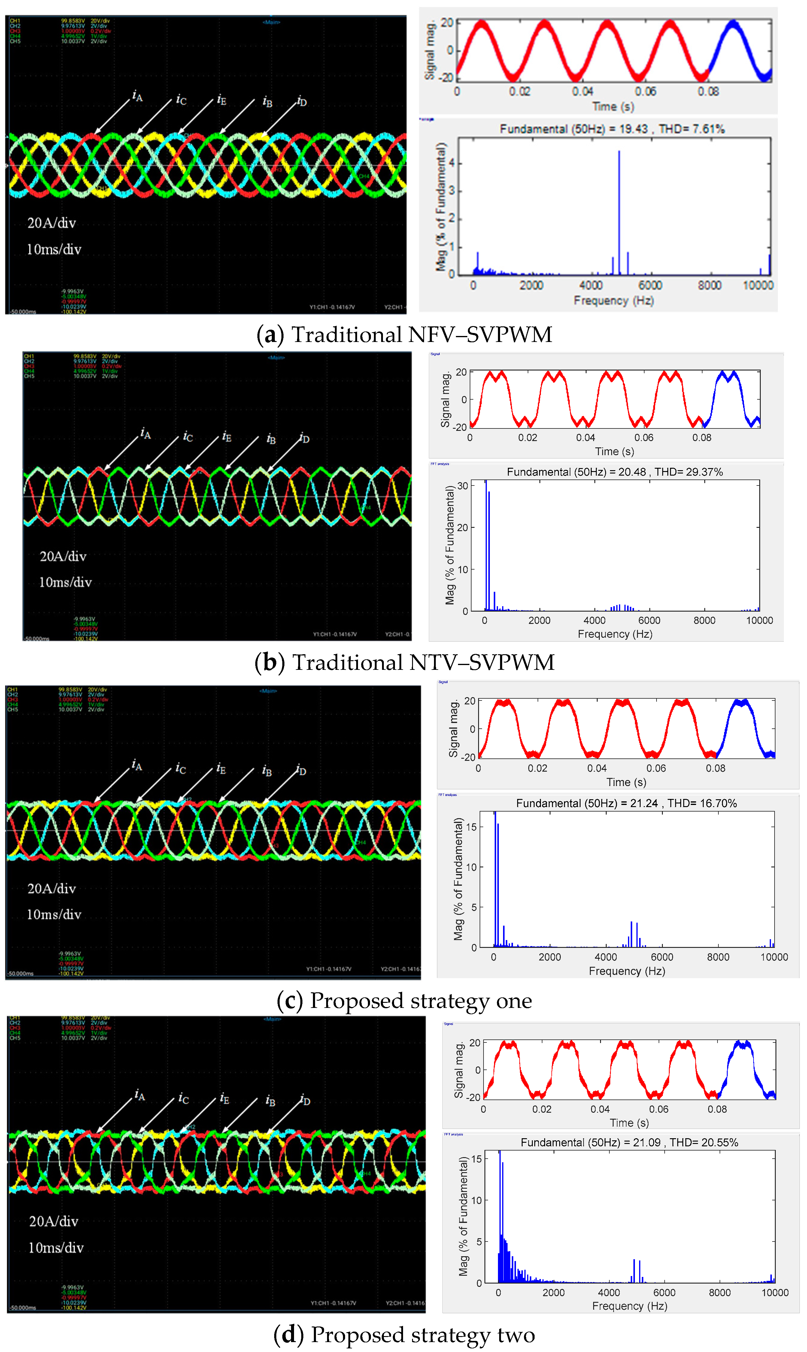
Figure 14.
The output phase voltage, phase current, and FFT spectrum under three modulation strategies with M = 0.95. (a) Traditional NFV–SVPWM. (b) Traditional NTV–SVPWM. (c) Proposed strategy one. (d) Proposed strategy two.
Figure 14.
The output phase voltage, phase current, and FFT spectrum under three modulation strategies with M = 0.95. (a) Traditional NFV–SVPWM. (b) Traditional NTV–SVPWM. (c) Proposed strategy one. (d) Proposed strategy two.


Table 1.
Amplitude of space voltage vector.
| Voltage Vector | Amplitude | |
|---|---|---|
| Large vector | U3, U6, U7, U12, U14, U17, U19, U24, U25, U28 | |
| Medium vector | U1, U2, U4, U8, U15, U16, U23, U27, U29, U30 | |
| Small vector | U5, U9, U10, U11, U13, U18, U20, U21, U22, U26 |
Table 2.
Simulation parameters.
| Parameter | Value |
|---|---|
| DC voltage/DC capacitance | 750 V/4700 uF |
| Output voltage/frequency | 380 V/50 Hz |
| R–L load | R = 20 Ω, L = 5 mH |
| Switching frequency fs | 5 kHz |
Table 3.
Comparison table of four modulation strategies.
| Comparative Indicators | NFV–SVPWM | NTV–SVPWM | Improved SVPWM Strategy I | Improved SVPWM Strategy II |
|---|---|---|---|---|
| Output voltage error | low | low | less | smaller |
| Total harmonic distortion (THD) | low | high | higher | lower |
| Modulation ratio (M) | 0.812 | inapplicable | 0.915 | 0.915 |
| Experimental validation results | practicable | practicable | practicable | practicable |
Disclaimer/Publisher’s Note: The statements, opinions and data contained in all publications are solely those of the individual author(s) and contributor(s) and not of MDPI and/or the editor(s). MDPI and/or the editor(s) disclaim responsibility for any injury to people or property resulting from any ideas, methods, instructions or products referred to in the content. |
© 2024 by the authors. Licensee MDPI, Basel, Switzerland. This article is an open access article distributed under the terms and conditions of the Creative Commons Attribution (CC BY) license (https://creativecommons.org/licenses/by/4.0/).
Share and Cite
MDPI and ACS Style
Jing, M.; Xia, Y.; Zhang, B. Research on Two Improved High–Voltage–Transfer–Ratio Space–Vector Pulse–Width–Modulation Strategies Applied to Five–Phase Inverter. Electronics 2024, 13, 1546. https://doi.org/10.3390/electronics13081546
AMA Style
Jing M, Xia Y, Zhang B. Research on Two Improved High–Voltage–Transfer–Ratio Space–Vector Pulse–Width–Modulation Strategies Applied to Five–Phase Inverter. Electronics. 2024; 13(8):1546. https://doi.org/10.3390/electronics13081546
Chicago/Turabian StyleJing, Mingchen, Yihui Xia, and Bin Zhang. 2024. "Research on Two Improved High–Voltage–Transfer–Ratio Space–Vector Pulse–Width–Modulation Strategies Applied to Five–Phase Inverter" Electronics 13, no. 8: 1546. https://doi.org/10.3390/electronics13081546
Note that from the first issue of 2016, this journal uses article numbers instead of page numbers. See further details here.