
Real-Time Defect Detection in Electronic Components during Assembly through Deep Learning

Technology Department, Cybord.ai, Tel-Aviv 6744332, Israel
*
Author to whom correspondence should be addressed.
Electronics 2024, 13(8), 1551; https://doi.org/10.3390/electronics13081551
Submission received: 29 February 2024
/
Revised: 12 April 2024
/
Accepted: 17 April 2024
/
Published: 19 April 2024
(This article belongs to the Special Issue Fault Detection Technology Based on Deep Learning)
Abstract
:This paper introduces a pioneering method for real-time image processing in electronic component assembly, revolutionizing quality control in manufacturing. By promptly capturing images from pick-and-place machines during the interval between component pick-up and mounting, defects are identified and promptly addressed in line. This proactive approach ensures that defective components are rejected before mounting, effectively preventing issues from ever occurring, thus significantly enhancing efficiency and reliability. Leveraging rapid network protocols such as gRPC and orchestration via Kubernetes, in conjunction with C++ programming and TensorFlow, this approach achieves an impressive average turnaround time of less than 5 milli-seconds. Rigorously tested on 20 operational production machines, it not only ensures adherence to IPC-A-610 and IPC-STD-J-001 standards but also optimizes production efficiency and reliability.
1. Introduction
The motivation for this work lies in the need to elevate the quality and reliability of electronic products while simultaneously reducing waste and extending the lifespan of electronic devices. Despite the importance of component quality, the electronic industry traditionally foregoes incoming inspection processes, relying instead on establishing trust with suppliers throughout the supply chain [1]. This trust-based approach assumes the absence of errors, fraud, counterfeits, damage, or defects in the procured materials, without employing dedicated technology for incoming inspections.
Despite often being subtle and barely perceptible to the naked eye, defects can have profound implications, particularly in applications governed by stringent standards and subjected to high stress levels [2,3]. Even the slightest imperfections, whether in a low-cost capacitor or a high-end processing unit, have the potential to trigger product malfunction [4,5,6,7,8,9,10]. It can be disheartening to witness the failure of a top-tier product due to an unnoticed defect in a seemingly inconspicuous component valued at just one cent.
Defects encompass a wide range of issues, spanning from cracks [11,12,13,14,15], fractures, and the peeling of metallization to deformations, discoloration, mold, corrosion [4,16,17,18,19,20,21,22,23], bent leads, deformed leads, and misshapen BGA balls, among others (see examples in Figure 1 and Figure 2). To provide clarity and establish a baseline for defect identification, leading standards such as IPC-A-610H [3] and IPC-STD-J-001 [24] offer comprehensive definitions of defects on assembled PCBs.
While significant technological advancements have been achieved in the assembly and testing stages of manufacturing [25,26], minimal attention has been given to technology focused on electronic components themselves. There exists a pervasive misconception that production machines such as pick-and-place and AOI (automated optical inspection) machines also monitor the quality of electronic components. However, these machines primarily track the assembly process and do not examine the components themselves for defects; they only detect deviations in how the components are placed. Consequently, only defects of considerable magnitude are typically identified, leading to a high tolerance for faults.
To tackle these challenges, extensive research and development endeavors have been undertaken by the authors. Initially, the focus was on combating counterfeit components, a prevalent issue during periods of electronic component shortages, notably observed in 2021–2023 and 2017–2018. Efforts were concentrated on performing a pre-inspection of reels procured from unauthorized distributors, posing a high risk of fraud. A method was devised to inspect all components within a reel while they remained sealed under the cover tape. The reels were inserted into a reel-to-reel inspection machine that rolled the tape while capturing images of each component in the reel. Utilizing images captured from the top side of the components and via a classification algorithm, manufacturers of components were identified based on their visual features [27]. This method was patented and published.
However, despite its high accuracy, this method necessitates using a reel-to-reel machine for the inspection of individual reels before they are utilized in production, limiting its applicability to only a fraction of the reels in use. The subsequent step aimed to enable the mass inspection of components and advance the concept of big data [28,29].
In order to facilitate the inspection of all electronic components, we leveraged the images captured by pick-and-place machines during their automated mounting process. These machines methodically pick up each component and measure their pick-up location and angle primarily using an automated vision system. Subsequently, the component is mounted on the PCB after compensating for pick-up inaccuracies. This process inherently captures images of all components from their bottom side just before they are mounted on the PCBs.
We seized these images from the machines and utilized them in conjunction with the algorithms developed for reel-to-reel machine models. As a typical production line processes, on average, around one million components a day, this provided the gateway to big data. Over the course of several years, we collected and analyzed approximately 4 billion components by deploying the system across tens of SMT (surface-mount technology) production lines [27,30,31,32,33]. The data were gathered and processed via a cloud platform capable of collecting from sites worldwide and centrally processing the data using cloud resources.
Our method for detecting counterfeits, defects, solderability issues, and corrosion was published in [27,30,31,32,33]. By applying this method to mass materials, we attained a unique position to evaluate the state of components from a statistical perspective. Consequently, we published work on the occurrence of corrosion and solderability issues in passive components [32]. Additionally, we documented several use cases of corrosion detected using this method, subsequently verified by lab analysis [16,34]. Moreover, we devised a method to mitigate the risk of cracks in MLCCs (multilayer ceramic capacitors) by the early detection of the evidence of corrosion in the soldering terminals as we demonstrated that corrosion serves as a precursor for crack development [12].
The accuracy and reliability of these methods are outlined in papers [30,31], relying extensively on big data. However, the presented method was centralized in the cloud and was suitable for the post-mounting detection of defects during production. Nonetheless, the delayed response time for uploading images to the cloud resulted in a reaction time of approximately 10 s, by which time the component was already on the PCB.
To address the imperative need for real-time reactions and to prevent the mounting of defective components, it became crucial to shift the processing to the edge near the mounting machines. The round trip of the image to the cloud would exceed the available time frame between pick-up and placement, which is measured in milliseconds. Therefore, the focus of this work is to present a method for performing real-time processing at the edge in a manner fast enough to react instantaneously and prevent the mounting of defective components within milliseconds.
The scope of this method extends to ensuring scalability to support multiple machines in production sites in an economical and reliable manner. This represents the pinnacle of this technology, enabling the electronic industry to exclusively utilize tested and qualified components. The impact it will have on industry efficiency, reliability, and quality is profound. This is because in today’s electronic landscape, most failures originate from the components themselves rather than from the manufacturing process.
The aim of this paper is to present the process of transitioning cloud-based algorithms to edge algorithms and to present the methodology and performance of this method. While the intricacies of the method have been elaborated in [32], we will provide an overview and underscore the differences between edge and cloud processing, emphasizing their significance for creating an efficient and nimble methodology.
In this work, we showcase how the processing of data at the edge, near the mounting machines, offers real-time insights and immediate actionability, contrasting with the delayed response time inherent in cloud processing. By introducing edge algorithms, we aim to address the critical need for instantaneous defect detection and prevention, particularly given the rapid pace of component mounting in electronic production lines.
Furthermore, we will explain the scalability and reliability of the edge-based method, essential for supporting multiple machines across production sites while maintaining economic feasibility. This shift from cloud to edge processing represents a pivotal advancement in technology, empowering the electronic industry to adopt a proactive approach to quality assurance and component integrity.
2. Compliance with IPC-A-610H and IPC-J-STD-001 Standards
The IPC-A-610H standard [3] serves as a comprehensive guide for assembled PCBs, outlining specific criteria for identifying defects and ensuring the quality of electronic assemblies. Other standards relate to the specific defect details as they appear in the IPC-A-610. In this section, we integrate the key compliance parameters outlined in IPC-A-610 with the presented AI-driven inspection method. In each section, we highlight the standard sections that are relevant to the presented method and that the method can detect automatically on all inspected components. The detection algorithm is only mentioned in this work and is elaborated in [12,16,30,32,34]. In this work, the novelty is in adapting the methods to real-time operation.
2.1. Defects on Component Leads/Terminations
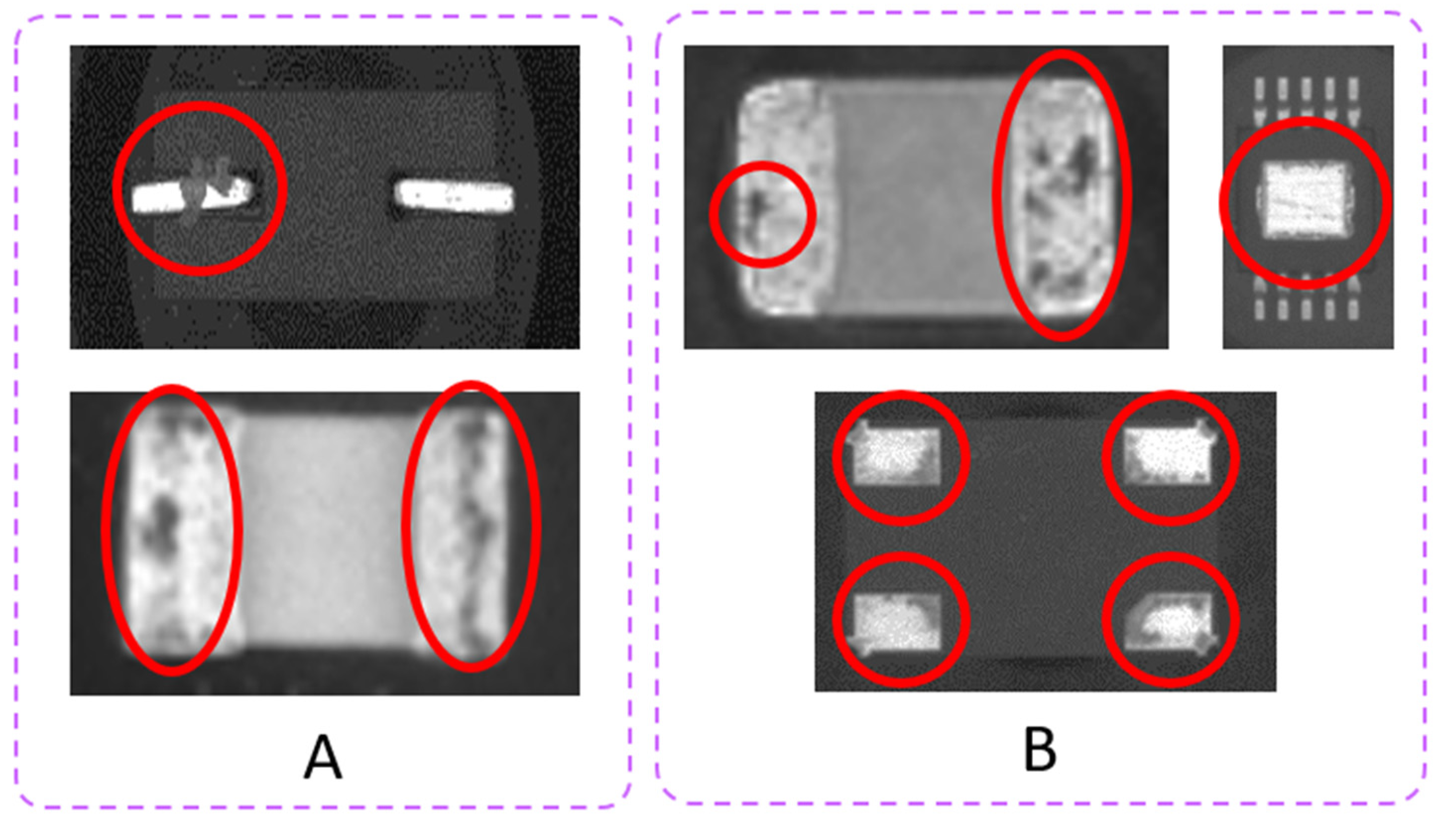
The examination of component leads is integral to our defect detection process, aligning with IPC-A-610’s criteria. Leveraging deep learning algorithms, the presented method scrutinizes each lead for damage or deformation exceeding 10% of the lead’s diameter, width, or thickness, ensuring compliance with IPC-A-610 standards. Examples from images taken by the pick-and-place machines and disqualified by the algorithm are presented in Figure 3. The deviations are circled. The visible defects are scratches, dents, distortions, deformations, peeling, shorts, etc.
2.2. Bent or Warped Leads
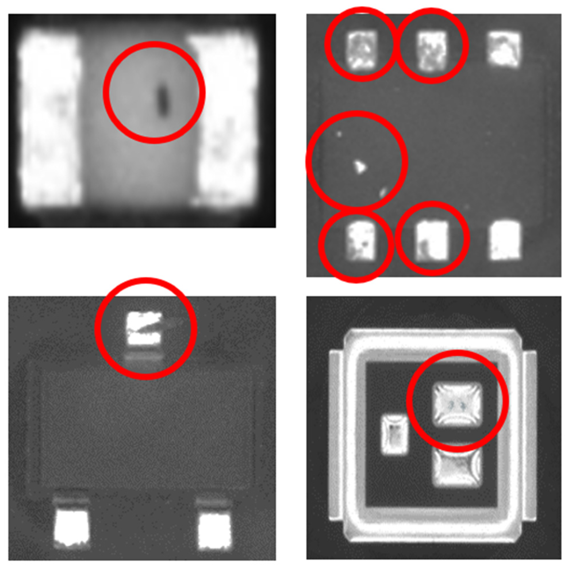
The presented method, powered by advanced deep learning techniques, is adept at identifying bending, indentation, and coplanarity issues in component leads, in accordance with IPC-A-610 Section 8.3.5.8. Through the presented advanced evaluation techniques, we ensure that any deviation beyond the specified threshold is promptly flagged for further assessment. Figure 4 presents examples of bent leads and coplanarity issues automatically detected by the algorithm that exceed 10% of the lead’s width.
2.3. Corrosion and Cleanliness
The presented method is equipped to detect corrosion and residues on metallic surfaces with precision. By promptly recognizing any indication of discoloration or evidence of corrosion, it ensures compliance with IPC-A-610 cleanliness and surface appearance parameters. Figure 5 presents examples of components with corrosion and contamination automatically detected by the AI algorithm that exceed 10% of the lead’s width.
2.4. Cleanliness—Foreign Object Debris (FOD)
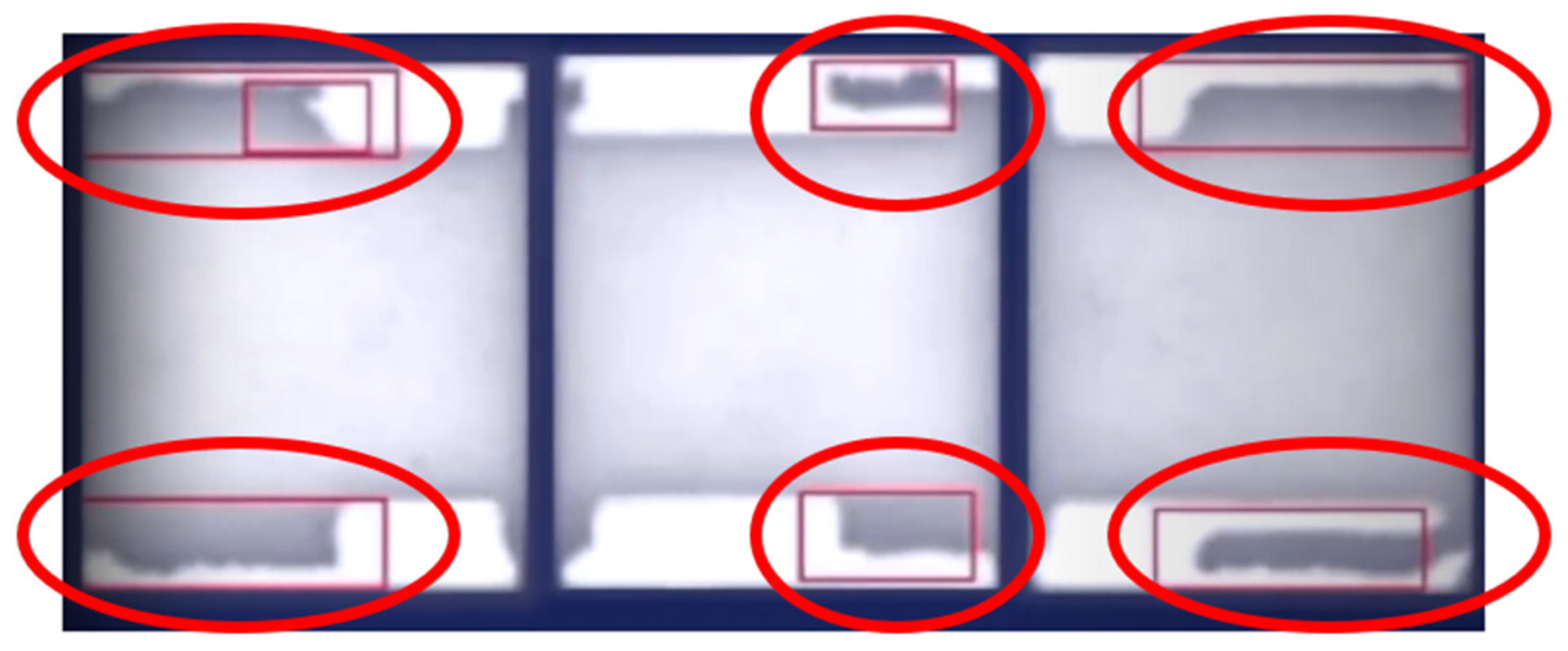
IPC-A-610 emphasizes the importance of cleanliness in electronic assemblies, particularly concerning foreign object debris (FOD). The presented method evaluates components for contamination, flagging any debris or residues beyond the specified threshold for further evaluation, in line with IPC-A-610 Section 10.6.2 and 10.6.3 standards. Figure 6 presents examples of components with corrosion and contamination automatically detected by the AI algorithm.
2.5. Loss of Metallization
Metallization loss defects are critical vulnerabilities highlighted by IPC-A-610 standards. The presented method identifies irregularities in metallization coverage, ensuring the optimal functionality and reliability of electronic components as per IPC-A-610 Section 9.1 and 9.3 standards. Figure 7 presents examples of components with metallization delamination automatically detected by the AI algorithm.
2.6. Mounting Upside Down
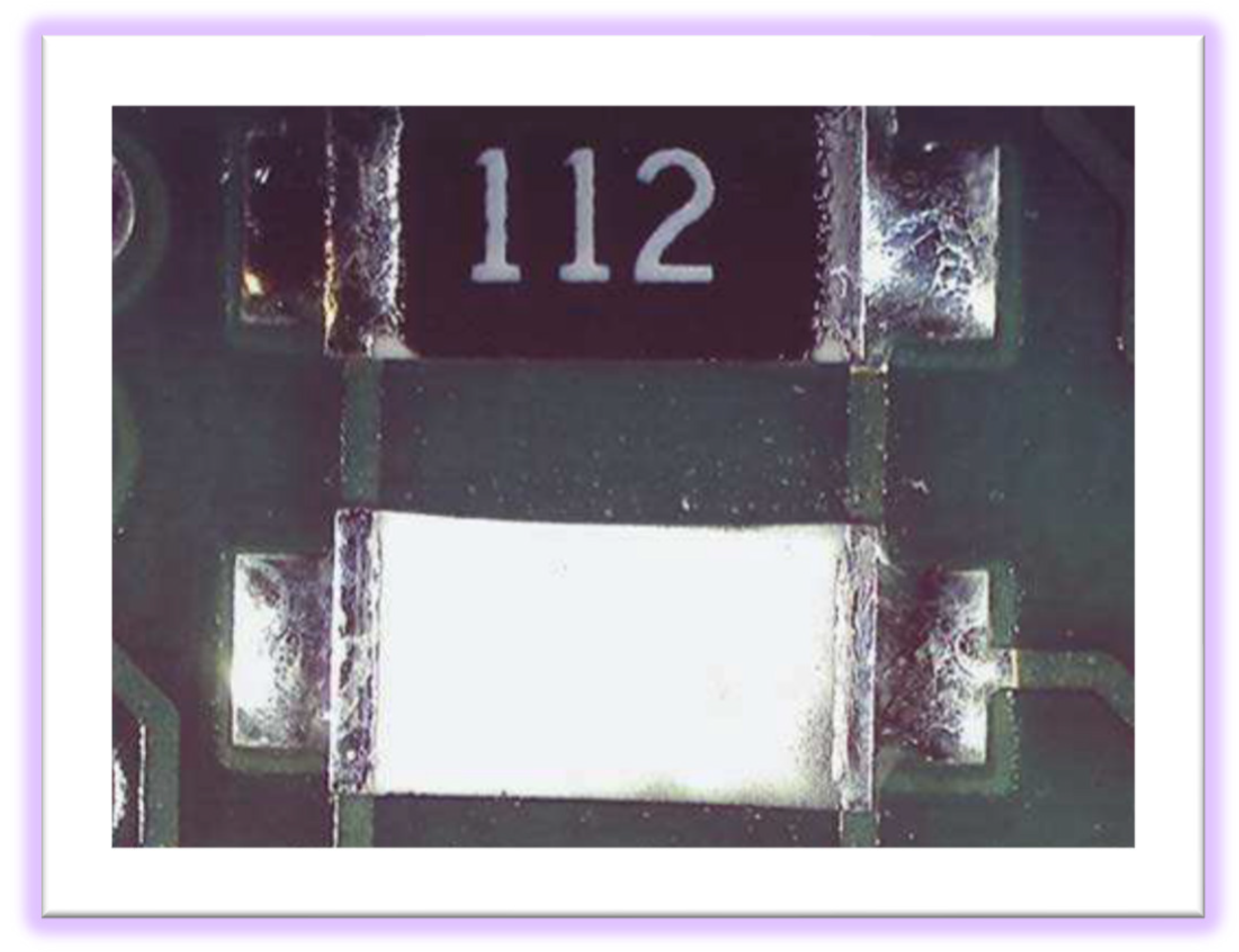
Lastly, the presented method is designed to detect components mounted upside down, as specified in IPC-A-610 Section 8.3.2.9.2. By flagging any non-compliant mounting configurations, our system ensures adherence to IPC-A-610 standards. Figure 8 presents a resistor mounted upside down from the top view.
In summary, the integration of advanced deep learning algorithms enhances the inspection system and seamlessly integrates IPC-A-610 compliance parameters, providing a robust framework for ensuring the quality and reliability of electronic components in accordance with industry standards.
3. Method
In this section, we explore the challenges our method must address to facilitate the real-time analysis of all assembled components. We outline the operational dynamics of pick-and-place machines, pinpointing the critical time window within which the method must react. Additionally, we detail the methodology employed to extract images from these machines, ensuring their availability for subsequent processing. Furthermore, we describe the pre-processing steps necessary for pre-processing the data before analysis.
3.1. Operational Workflow and Critical Points in Pick-and-Place Component Handling
The schematic in Figure 9 describes the operational flow, depicting the sequence from image capture to component placement. This visual aid highlights intervention points and the execution of directives for component rejection. Emphasizing the time window underscores the significance of timely actions in maintaining the quality and reliability of the assembly process. Notably, the response time window varies from 10 to 30 milliseconds, contingent upon the specific machine model.
The component shooters retrieve 20 to 28 components in a single run. They encompass two primary families: the revolver pick-up head, characteristic of ASMPT (Singapore) and Fuji (Japan), proficient in component retrieval via a revolving head, and the cluster-based pick-up head typical to Panasonic (Japan) and Yamaha (Japan), equipped with multiple nozzles, sequentially retrieving components before traversing a pit camera. While quick, shooters are primarily suited for smaller components, resulting in relatively diminutive image sizes and abbreviated processing times. In contrast, pick-and-place heads, designed for larger components, collect a lesser quantity per run, albeit necessitating more time for processing due to the larger component dimensions. These divergent parameters strike a balance, resulting in comparable speed requirements across all pick-up heads.
The pick-and-place machine captures component images to determine their positioning on the pick-up nozzle, enabling precise placements and compensating for minor positional inaccuracies. Furthermore, it identifies incorrect pick-ups, such as empty nozzles or tombstone pick-ups in conjunction with the vacuum sensor in the pick-up nozzle. Traditional machine vision tools process these images between pick-up and placement time. Any deviation from acceptable pick-up thresholds prompts the vision software to flag the component for rejection, subsequently leading to its disposal in a designated bin.
3.2. Data Collection from the Pick-and-Place Machine
Data collection from the pick-and-place machine is performed through a dedicated application programming interface (API), designed to streamline the transfer of images and metadata from the machine to a local server. The data collection process is based on a REST API integrated into the pick-and-place machine, which interfaces with the machine’s image capture system. It orchestrates the acquisition of data in a format conducive to real-time analysis, fetching images of components milliseconds before their placement on the PCB. Additionally, the API collates metadata associated with each image, providing contextual information for subsequent analysis.
The data from the API undergo transmission to a local server using the Google Remote Procedure Call (GRPC) protocol. Employing GRPC is a rapid method to transfer the images and metadata from the pick-and-place machine to the local server. This protocol’s proficiency in real-time applications ensures minimal latency and maximal throughput, critical for prompt defect and corrosion detection. The exchange of data between the pick-and-place machine and the local server occurs within the local network.
3.3. Pre-Processing
The effectiveness of the real-time defect and corrosion detection system relies on a series of procedures, including pre-processing, feature extraction, and the selection of an appropriate model architecture. The following sections present each of these steps in detail.
Beginning with centering and cropping, the pre-processing workflow ensures the accurate alignment and framing of component images. This step aligns the component centrally within the image frame and crops it uniformly to facilitate consistent and accurate analysis. Figure 10 illustrates instances where the algorithm must disregard certain aspects due to the pick-and-place machine’s ability to address them. It also highlights challenges posed by off-center component images, emphasizing precise processing.
Light balance correction rectifies lighting irregularities within images to ensure an accurate analysis. A specialized classifier identifies images with lighting discrepancies, particularly those afflicted by saturation. Upon detection, the system prompts the machine to make necessary adjustments. Rectifying these imbalances is important as saturated images impede analysis and compromise component placement accuracy. Figure 11 exemplifies a component with excessive light balance, underscoring the importance of this correction process.
In addition to light balance concerns, the pre-processing stage involves identifying and rectifying blurry images, which can impede component placement and inspection accuracy. Blurriness often results from incorrect programming or defective lighting and imaging systems, necessitating prompt detection and mitigation. Addressing blurry images early is important to ensure a reliable and accurate analysis. Figure 12 illustrates an example of a blurry image captured during component inspection, emphasizing the importance of early detection and mitigation during pre-processing.
Metadata matching is used for gaining an understanding of the component’s package type. This insight enables the categorization of components based on their visual similarities. For instance, in the case of passive chip components like chip resistors, classification is determined by functionality and footprint. For example, a chip resistor with a size of 0603 is denoted as CRES-0603. It is important to note that the algorithm does not require specific resistor values or part numbers for analysis. Instead, our approach focuses on identifying and categorizing components based on production lines and visual characteristics.
3.4. Model Architecture for Defect and Corrosion Detection
The algorithm is presented in [12,16,30,32,34] in detail. In this work, we present the gap to edge real-time computing. The objective is to categorize images as either “normal” or “defective”, with potential nuances such as minor, moderate, or major defects in some instances. Initial attempts to address this classification challenge leaned towards leveraging popular ImageNet models; however, these endeavors encountered two primary hurdles.
A significant challenge arises from the scarcity of training data available within the realm of electronic components. The prevalence of defective items is notably low, often amounting to less than one defect per ten thousand components [30]. Acquiring an adequate number of defective items to establish a robust training dataset proves arduous. In scenarios where only a few hundred defective items exist among millions of components, conventional image classification models tend to grapple with overfitting. Overfitting leads to situations where training accuracy reaches 100%, but validation accuracy remains notably lower, sometimes failing to surpass that of random guessing.
Another challenge revolves around the resemblance between some defective items and their normal counterparts. Defects and corrosion can manifest subtly, such as small dots within components. Conventional convolutional neural network (CNN) models often falter in identifying these inconspicuous defects and corrosion due to their limited capacity to capture fine-grained details [34].
We introduce a specialized network architecture tailored for defect and corrosion detection, as detailed in [32,33] (see Figure 13). Unlike the serial architecture commonly found in popular image classification models, where multiple layers of small filters, typically 3 × 3 in size, are connected sequentially, our approach adopts a set of filters with varying window sizes operating in parallel. Each filter within this set is designed to detect a specific type of defective region or corrosion within component images. These filters generate features indicating the likelihood of such defects and corrosion being present. The overall feature vector is formed by concatenating all the individual features produced by these parallel filters. Subsequently, this feature vector undergoes processing through a dense layer, culminating in the final defect and corrosion score (see Figure 13).
Moreover, we employ data augmentation techniques during training to enhance network performance. These techniques involve artificially expanding the training dataset by applying transformations like rotation, flipping, and scaling to existing images. By generating variations of the original data, augmentation mitigates overfitting and enhances the model’s ability to generalize to unseen data, enabling learning from a more diverse range of examples.
The adoption of this parallel architecture not only enhances defect and corrosion detection accuracy but also improves algorithm efficiency. It facilitates high-speed processing, capable of analyzing up to 3000 images per second on a Tesla T4 GPU. This GPU acceleration yields a substantial reduction in processing time, rendering the system suitable for real-time inspection during the component assembly process. By optimizing the architecture for GPU support, the algorithm capitalizes on the parallel processing capabilities of the GPU, swiftly performing image analysis. The combined benefits of this architecture and GPU acceleration ensure efficient and timely defect and corrosion detection, further elevating the overall quality of electronic products.
3.5. Comparative Analysis: Benchmarking against Other Defect Detection Methods
To gauge the effectiveness of the proposed defect detection approach, we conducted a comparative analysis against robust principal component analysis (RPCA) [35,36,37,38], a widely used method for anomaly detection. Both approaches were evaluated on diverse datasets comprising various component types to ascertain their accuracy and recall rates, reflective of their defect detection capabilities. The methods were tested using a small batch of previously labeled components, with defects verified through visual and lab inspection. It is important to highlight that the dataset used in our study encompasses various levels of defects, with the primary focus being on identifying defects that may lead to a decrease in reliability.
We initially tested RPCA on datasets containing three component types: capacitor, resistor, and SOT-23-3. Table 1 summarizes the results. Using the same datasets, we evaluated our model, and the results are presented in Table 2.
The presented model consistently outperforms RPCA in terms of both accuracy and recall across all component types. While RPCA yields acceptable results for some components, particularly SOT-23-3, it demonstrates poor performance for passive components like the capacitor and resistor. In contrast, our model delivers consistently high accuracy and recall rates across various component types, highlighting its effectiveness in defect detection.
4. Advancements to Real-Time Processing
In the traditional approach, data collection involved capturing component images and associated metadata, which were subsequently transmitted to cloud servers for processing [30]. However, this cloud-based analysis faced a significant drawback: processing times averaging around 10 s per component. Earlier iterations also encountered delays in defect and corrosion detection due to batch processing of similar components, primarily caused by the time required for data transfer to and from the cloud.
The method presented in this study prioritizes real-time defect and corrosion detection by relocating the processing center. Instead of relying on cloud-based analysis, this approach emphasizes edge computing, ensuring that processing occurs directly at the point of data acquisition. To meet the speed required for real-time defect and corrosion detection, the method utilizes graphics processing units (GPUs) and refines algorithms and software capable of operating within stringent timeframes.
Achieving real-time processing for deep neural network (DNN) classification models on edge devices, such as MobileNet, necessitates exploring techniques and tools to enhance processing speed. Quantization involves reducing the precision of model weights and activations, typically transitioning from 32-bit floating-point numbers to 8-bit fixed-point numbers. This reduction reduces memory usage and computational demands, facilitating swifter inference, particularly beneficial for resource-constrained edge devices. However, it may lead to a reduction in model accuracy due to diminished precision.
Model pruning involves eliminating non-essential weights or neurons from the neural network, resulting in a more streamlined and expedited model. Pruning reduces the model’s size, leading to quicker inference times and a smaller memory footprint. However, it requires careful handling to prevent accuracy loss and may introduce some model instability. Depthwise separable convolutions (DSCs) split the convolution process into two stages, reducing computational cost, and they are commonly used in architectures like MobileNet for efficient inference on mobile and edge devices. Additionally, model parallelism divides the model into smaller segments, each processed in parallel on distinct GPUs, potentially achieving linear speedup with additional GPUs, particularly valuable for intricate models with high computational demands.
Operator fusion amalgamates multiple mathematical operations into a single operation, mitigating overheads associated with memory transfers and kernel launches on GPUs, thereby augmenting inference speed. The ONNX Runtime serves as an inference engine optimized for executing ONNX models, furnishing high-performance inferencing across diverse hardware platforms, including GPUs.
These methods reduce model size and enhance inference speed while maintaining an acceptable level of accuracy. TensorFlow, with its comprehensive support for quantization and model optimization, emerges as a practical platform for implementing these optimizations. Additionally, ONNX Runtime can be leveraged for efficient inference on edge devices, enabling real-time inference on the edge for the rapid and precise execution of MobileNet-like models for electronic component inspection.
5. Architectural Framework and Deployment Strategies
This section provides an in-depth exploration of the architectural framework of the solution and the strategies implemented to optimize its performance and reliability. The architecture, illustrated in Figure 14 and elaborated in Table 3, demonstrates its effectiveness in overcoming challenges related to limited training data and the identification of subtle defects and corrosion in electronic components during the assembly process. This approach offers an efficient, data-efficient solution for defect and corrosion detection, ultimately enhancing product quality and reliability.
The solution harnesses Kubernetes to orchestrate services across multiple servers at each customer’s site, enhancing system robustness and scalability. Machine learning models are stored in cloud storage, allowing for on-demand retrieval during software startups. These models are securely encrypted in memory to ensure controlled access. An external process continually monitors changes in remote storage, prompting the system to fetch updates and deploy the most current models.
Operating on Dell servers equipped with Nvidia RTX GPUs, the system adopts a software as a service (SaaS) model. Data transmission occurs through the gRPC protocol, while model execution is facilitated by C++ TensorFlow Serving. The architectural design efficiently processes asynchronous data from all machines at the site, enabling the concurrent execution of two AI models for each component. Commands are issued to deactivate the components only when necessary.
Figure 15 illustrates the Kubernetes cluster, based on Nvidia’s GPU, scaling to accommodate multiple production machines and growing production demands. This visualization underscores the system’s scalability and adaptability to evolving operational requirements.
6. Experimental Setup and Evaluation
This section describes the experimental setup employed to evaluate the solution’s performance and capabilities. The experiments encompassed a range of hardware configurations and software optimizations aimed at evaluating its potential in real-world electronic component assembly scenarios. We utilized the Nvidia RTX 3070 server, featuring 8 GB of DDR6 RAM and 16 cores, as the foundational server for our tests.
To simulate real-world conditions, we first replicated an environment mirroring a production line setup, comprising 20 pick-and-place (P&P) machines continuously dispatching components via the gRPC protocol. Our experimentation extended to exploring Nvidia’s A100 and L4 GPUs to evaluate adaptability to different GPU configurations. C++ served as our primary programming language. We conducted comparative assessments to discern performance differences between different versions. Additionally, we employed TensorRT, a deep learning inference optimizer and runtime library developed by NVIDIA. The integration of TensorRT enabled the analysis of performance and efficiency of machine-learning models on GPUs, contributing to understanding the solution’s capabilities in real-time electronic component inspection.
6.1. Benchmarking and Testing
In order to quantitively assess the performance of the presented solution in real-world production environments, we engineered an environment mirroring the configurations commonly found in our customers’ setups. This environment was designed to incorporate 20 ASMPT pick-and-place (P&P) machines, each mounting components and utilizing the gRPC protocol. This stress testing was important in gauging the solution’s robustness and reliability in handling the demands of large-scale electronic component inspections. Over 1.6 million components were processed within a data frame over 12 h.
In addition to hardware evaluations, the software underwent thorough testing and refinement. Developed from the ground up using C++, our software underwent comparisons between different versions to ensure optimal performance and reliability. To further enhance the understanding of the presented solution’s capabilities, we subjected our machine learning models to testing using TensorRT, an advanced deep learning inference optimizer and runtime library developed by NVIDIA. The evaluation of our models on GPUs, along with detailed performance metrics, is presented in the following section, providing valuable insights into the efficiency and effectiveness of our solution in real-time electronic component inspections.
6.2. Pre-Processing Stage Evaluation
In the pre-processing stage, all images underwent initial processing for light balancing (clipping), aiming to address issues related to images with a high ratio of saturated pixels. These saturated pixels are indicators that the mounting machine can be utilized to enhance the accuracy of component placement. See examples in Figure 11, where the frequency of clipped images during the system’s operation on real-time data is depicted. It is evident that approximately 4.6 components per second are clipped in this scenario. However, as the system continuously conveys this information to the mounting machine, there is a reduction in this rate over time due to the feedback loop. This feedback mechanism contributes to improving the accuracy of placement and reducing the attrition rate in the assembly process.
In addition to addressing issues related to clipped images, the pre-processing stage also mitigates problems associated with blurry images, which can significantly impact mounting accuracy and increase attrition rates. Blurry images often occur due to incorrect programming that fails to allocate a sufficient resolution (binning) to the image, resulting in a lack of sharpness (as observed in Figure 12). Another common cause of blurry images is the incorrect programming of component height, leading to poor focus during image capture. Defective lighting or imaging systems can also contribute to image blurriness.
6.3. Pre-Processing Stage—Component Dimensions Measurement
In high-volume production lines, accurately measuring the dimensions of mounted components is crucial due to the wide variety of component sizes encountered. Figure 16 displays the calculated width and height of mounted components over a 12 h interval during testing. The data reveal that small passive components such as MLCCs and chip resistors are the most prevalent size category. We have observed a positive correlation between the size of the image and the end-to-end processing time, indicating that larger images take longer to process.
Obtaining real-life dimensions of components and calculating the mean and variance of their sizes are vital steps in improving the performance of pick-and-place (P&P) and automated optical inspection (AOI) systems. These measurements provide accurate feedback for programming component dimensions, enhancing the software’s performance by relying on real measurements of specific components rather than generic information from tables or specification sheets.
Furthermore, analyzing the variance in component sizes is essential for assessing the quality of materials used and the consistency of components within each container. Variance measurements help gauge how similar the components are within a batch, providing insights into manufacturing quality and potential issues related to component variation.
6.4. Processing Stage—Component Defects and Corrosion Detection Algorithms
The experiment involved running both the defect and corrosion detection algorithms simultaneously, while 20 machines operated asynchronously in a real-world production environment. The primary focus was to evaluate the processing time of these algorithms under high-volume conditions. During the experiment, the mean processing time for defect and corrosion detection algorithms was approximately 1.5 milliseconds per component and approximately 20 components per second. Figure 17 presents the processing time of the defects detection algorithm and the corrosion detection algorithm, running in parallel on the same images. Note that the presented processing time solely accounts for the time spent on the detection algorithms and excludes pre-processing steps and network delays. These results demonstrate the efficiency and effectiveness of the implemented algorithms in real-time defect and corrosion detection. The size of the components significantly impacts processing performance.
7. Conclusions
We introduce a groundbreaking method for the real-time processing of images during SMT assembly, representing a significant advancement in quality control within manufacturing environments. Our approach enables a 100% inspection of all components, virtually eliminating visible defective components from the final products through an inline process. Moreover, the method ensures compliance with industry-leading standards such as IPC-A-610 and IPC-STD-J-001.
By leveraging the time window between component pick-up and mounting, our method ensures real-time image processing with an average turnaround time of less than 5 milliseconds. This efficiency is facilitated by utilizing the gRPC network protocol and Kubernetes orchestration for coordination across production environments. The implementation of C++ programming, real-time TensorFlow, and cost-effective GPU further enhances the method’s speed and reliability.
In addition to the advancements highlighted, the presented method incorporates a system for image acquisition and analysis, supported by AI and big data technologies. Images of the components during SMT assembly are captured using cameras already installed within the production line, ensuring a detailed visual inspection of each component. These images are then processed in real-time through our AI-driven algorithms, leveraging the power of deep learning and big data analytics to detect defects and anomalies with exceptional accuracy.
The transition from traditional cloud-based processing to real-time edge processing is facilitated by a specialized architecture and software design. By deploying Kubernetes orchestration, we have streamlined the coordination of processing tasks across distributed edge devices, optimizing resource utilization and minimizing latency. The adoption of C++ programming, coupled with real-time TensorFlow inference and cost-effective GPU acceleration, further enhances the speed and reliability of our solution, enabling its seamless integration into existing manufacturing workflows.
Through rigorous testing on 20 live production machines, we have validated the scalability and effectiveness of our approach in real-world manufacturing settings. By achieving 100% inspection coverage and virtually eliminating defective components from the final products, our method sets a new standard for quality control in SMT assembly.
Author Contributions
Conceptualization, E.W.; Software, S.C. and M.S.; Investigation, E.W. and K.H.; Writing—original draft, E.W.; Writing—review & editing, E.W., S.C. and K.H. All authors have read and agreed to the published version of the manuscript.
Funding
This research was partially funded by the Israel Innovation Authority grant number 81349.
Data Availability Statement
Data is available at cybord.ai/resources/#Scholarly%20Articles.
Conflicts of Interest
All authors were employed by the company Cybord.ai. They declare that the research was conducted in the absence of any commercial or financial relationships that could be construed as a potential conflict of interest.
References
- Goel, A.; Graves, R.J. Electronic system reliability: Collating prediction models. IEEE Trans. Device Mater. Reliab. 2006, 6, 258–265. [Google Scholar] [CrossRef]
- Băjenescu, T.I.; Băjenescu, T.-M.I.; Bâzu, M.I. Component Reliability for Electronic Systems; Artech House: London, UK, 2010. [Google Scholar]
- IPC-A-610 Acceptability of Electronic Assemblies. Revision J. 2024. Available online: www.ipc.org (accessed on 1 April 2024).
- Yadav, A.; Gupta, K.K.; Ambat, R.; Christensen, M.L. Statistical analysis of corrosion failures in hearing aid devices from tropical regions. Eng. Fail Anal. 2021, 130, 105758. [Google Scholar] [CrossRef]
- Joshy, S.; Verdingovas, V.; Jellesen, M.S.; Ambat, R. Circuit analysis to predict humidity related failures in electronics—Methodology and recommendations. Microelectron. Reliab. 2019, 93, 81–88. [Google Scholar] [CrossRef]
- Piotrowska, K.; Verdingovas, V.; Ambat, R. Humidity-related failures in electronics: Effect of binary mixtures of weak organic acid activators. J. Mater. Sci. Mater. Electron. 2018, 29, 17834–17852. [Google Scholar] [CrossRef]
- Burton, L.C. Intrinsic Mechanisms of Multi-Layer Ceramic Capacitor Failure; Department of Electrical Engineering and Materials Engineering: Richmond, VA, USA, 1984. [Google Scholar]
- Zhang, H.; Liu, Y.; Wang, J.; Sun, F. Failure study of solder joints subjected to random vibration loading at different temperatures. J. Mater. Sci. Mater. Electron. 2015, 26, 2374–2379. [Google Scholar] [CrossRef]
- Kishore, K. On the crucial role of the on-site and visual observations in failure analysis and prevention. J. Fail. Anal. Prev. 2021, 21, 1126–1132. [Google Scholar] [CrossRef]
- Ohring, M.; Kasprzak, L. Chapter 9-degradation of contacts and package interconnections. In Reliability and Failure of Electronic Materials and Devices; Ohring, M., Ed.; Academic Press: Hoboken, NJ, USA, 1998; pp. 475–537. [Google Scholar]
- Jiang, B.; Bai, Y.; Cao, J.L.; Su, Y.; Shi, S.Q.; Chu, W.; Qiao, L. Delayed crack propagation in barium titanate single crystals in humid air. J. Appl. Phys. 2008, 103, 116102. [Google Scholar] [CrossRef]
- Weiss, E. Detecting Corrosion to Prevent Cracks in MLCCs with AI. J. Fail. Anal. Prev. 2023, 24, 50–57. [Google Scholar] [CrossRef]
- Johnson, W.L.; Kim, S.A.; White, G.S.; Herzberger, J. Nonlinear resonant acoustic detection of cracks in multilayer ceramic capacitors. In IEEE International Ultrasonics Symposium, IUS; IEEE Computer Society: Washington, DC, USA, 2014; pp. 244–247. [Google Scholar] [CrossRef]
- Teverovsky, A.; Gov, A.A.T. NASA Electronic Parts and Packaging (NEPP) Program NEPP Task: Guidelines for Selection of Ceramic Capacitors for Space Applications Cracking Problems in Low-Voltage Chip Ceramic Capacitors Cracking Problems in Low-Voltage Chip Ceramic Capacitors. Available online: https://ntrs.nasa.gov/api/citations/20190001592/downloads/20190001592.pdf (accessed on 1 April 2024).
- Andersson, C.; Ingman, J.; Varescon, E.; Kiviniemi, M. Detection of cracks in multilayer ceramic capacitors by X-ray imaging. Microelectron. Reliab. 2016, 64, 352–356. [Google Scholar] [CrossRef]
- Weiss, E. Preventing Corrosion-related Failures in Electronic Assembly: A Multi-case Study Analysis. IEEE Trans. Compon. Packag. Manuf. Technol. 2023, 13, 743–749. [Google Scholar] [CrossRef]
- Ambat, R.; Conseil-Gudla, H.; Verdingovas, V. Corrosion in electronics. In Encyclopedia of Interfacial Chemistry: Surface Science and Electrochemistry; Elsevier: Amsterdam, The Netherlands, 2018; pp. 134–144. [Google Scholar] [CrossRef]
- Comizzoli, R.B.; Frankenthal, R.P.; Milner, P.C.; Sinclair, J.D. Corrosion of electronic materials and devices. Science 1986, 234, 340–345. [Google Scholar] [CrossRef] [PubMed]
- Hienonen, R.; Lahtinen, R. Corrosion and Climatic Effects in Electronics; VTT Technical Research Centre of Finland: Espoo, Finland, 2000. [Google Scholar]
- See, C.W.; Yahaya, M.Z.; Haliman, H.; Mohamad, A.A. Corrosion Behavior of Corroded Sn–3.0Ag–0.5Cu Solder Alloy. Procedia Chem. 2016, 19, 847–854. [Google Scholar] [CrossRef]
- Sinclair, J.D. Corrosion of Electronics the Role of Ionic Substances. J. Electrochem. Soc. 1988, 135, 89C. [Google Scholar] [CrossRef]
- Sonawane, P.D.; Raja, V.K.B. An overview of corrosion analysis of solder joints. In AIP Conference Proceedings; American Institute of Physics Inc.: College Park, MD, USA, 2020. [Google Scholar] [CrossRef]
- Li, S.; Wang, X.; Liu, Z.; Jiu, Y.; Zhang, S.; Geng, J.; Chen, X.; Wu, S.; He, P.; Long, W. Corrosion behavior of Sn-based lead-free solder alloys: A review. J. Mater. Sci. Mater. Electron. 2020, 31, 9076–9090. [Google Scholar] [CrossRef]
- IPC-STD-J-001. Requirements for Soldered Electrical and Electronic Assemblies. Revision J. 2024. Available online: www.ipc.org (accessed on 1 April 2024).
- Pongboonchai-Empl, T.; Antony, J.; Garza-Reyes, J.A.; Komkowski, T.; Tortorella, G.L. Integration of Industry 4.0 technologies into Lean Six Sigma DMAIC: A systematic review. Prod. Plan. Control. 2023, 1–26. [Google Scholar] [CrossRef]
- Zheng, T.; Ardolino, M.; Bacchetti, A.; Perona, M. The applications of Industry 4.0 technologies in manufacturing context: A systematic literature review. Int. J. Prod. Res. 2021, 59, 1922–1954. [Google Scholar] [CrossRef]
- Weiss, E. System and Method for Detection of Counterfeit and Cyber Electronic Components. 2019. Available online: https://patents.google.com/patent/WO2020202154A1/en (accessed on 1 April 2024).
- Wang, J.; Xu, C.; Zhang, J.; Zhong, R. Big data analytics for intelligent manufacturing systems: A review. J. Manuf. Syst. 2022, 62, 738–752. [Google Scholar] [CrossRef]
- Zhao, W.; Gurudu, S.R.; Taheri, S.; Ghosh, S.; Sathiaseelan, M.A.M.; Asadizanjani, N. PCB Component Detection Using Computer Vision for Hardware Assurance. Big Data Cogn. Comput. 2022, 6, 39. [Google Scholar] [CrossRef]
- Weiss, E. AI Detection of Body Defects and Corrosion on Leads in Electronic Components, and a study of their Occurrence. In Proceedings of the 2022 IEEE International Symposium on the Physical and Failure Analysis of Integrated Circuits (IPFA), Singapore, 18–21 July 2022; pp. 1–6. [Google Scholar]
- Weiss, E. Counterfeit Mitigation by In-Line Deep Visula Inspection. SMTA. Available online: http://iconnect007.uberflip.com/i/1440051-smt007-jan2022/87? (accessed on 1 April 2024).
- Weiss, E. Electronic Component Solderability Assessment algorithm by Deep External Visual Inspection. In Proceedings of the 2020 IEEE Physical Assurance and Inspection of Electronics (PAINE), Washington, DC, USA, 15–16 December 2020; pp. 1–6. [Google Scholar]
- Weiss, E.; Efrat, Z. System and Method for Nondestructive Assessing of Solderability of Electronic Components. US20230129202A1, 8 April 2021. [Google Scholar]
- Weiss, E. Revealing Hidden Defects in Electronic Components with an AI-Based Inspection Method: A Corrosion Case Study. IEEE Trans. Compon. Packag. Manuf. Technol. 2023, 13, 1078–1080. [Google Scholar] [CrossRef]
- Cao, J.; He, H.; Zhang, Y.; Zhao, W.; Yan, Z.; Zhu, H. Crack detection in ultrahigh-performance concrete using robust principal component analysis and characteristic evaluation in the frequency domain. Struct. Health Monit. 2024, 23, 1013–1024. [Google Scholar] [CrossRef]
- Schreiber, J.B. Issues and recommendations for exploratory factor analysis and principal component analysis. Res. Soc. Adm. Pharm. 2021, 17, 1004–1011. [Google Scholar] [CrossRef]
- Pesaresi, S.; Mancini, A.; Quattrini, G.; Casavecchia, S. Mapping mediterranean forest plant associations and habitats with functional principal component analysis using Landsat 8 NDVI time series. Remote Sens. 2020, 12, 1132. [Google Scholar] [CrossRef]
- Machidon, A.L.; Del Frate, F.; Picchiani, M.; Machidon, O.M.; Ogrutan, P.L. Geometrical approximated principal component analysis for hyperspectral image analysis. Remote Sens. 2020, 12, 1698. [Google Scholar] [CrossRef]
Figure 1.
Examples on passive components (left to right): conductive FOD (foreign object debris), corrosion leading to cracks, lead peeling, non-conductive FOD.
Figure 1.
Examples on passive components (left to right): conductive FOD (foreign object debris), corrosion leading to cracks, lead peeling, non-conductive FOD.

Figure 2.
Examples on leaded components (left to right): FOD, termination peeling, bent leads, distorted leads.
Figure 2.
Examples on leaded components (left to right): FOD, termination peeling, bent leads, distorted leads.

Figure 3.
Examples from images taken by the pick-and-place machines and disqualified by the algorithm. Detected defects are highlighted in red circles.
Figure 3.
Examples from images taken by the pick-and-place machines and disqualified by the algorithm. Detected defects are highlighted in red circles.

Figure 4.
Examples of bent leads and coplanarity issues automatically detected by the algorithm that exceed 10% of the lead’s width. Detected defects are highlighted in red circles. (A) Bent leads, (B) deformed leads, (C) damaged leads.
Figure 4.
Examples of bent leads and coplanarity issues automatically detected by the algorithm that exceed 10% of the lead’s width. Detected defects are highlighted in red circles. (A) Bent leads, (B) deformed leads, (C) damaged leads.

Figure 5.
Examples of components with corrosion and contamination automatically detected by the AI algorithm that exceed 10% of the lead’s width. Detected defects are highlighted in red circles. (A) Contamination of leads, (B) corrosion of leads.
Figure 5.
Examples of components with corrosion and contamination automatically detected by the AI algorithm that exceed 10% of the lead’s width. Detected defects are highlighted in red circles. (A) Contamination of leads, (B) corrosion of leads.

Figure 6.
Examples of components with corrosion and contamination automatically detected by the AI algorithm. Detected defects are highlighted in red circles. Note that debris may be due to a component defect or point out a root cause in the supply chain, such as contaminated components in a container or poorly handled material.

Figure 7.
Examples of components with metallization delamination automatically detected by the AI algorithm. Detected defects are highlighted in red circles.
Figure 7.
Examples of components with metallization delamination automatically detected by the AI algorithm. Detected defects are highlighted in red circles.

Figure 8.
A resistor mounted upside down from the top view.

Figure 9.
Process flow of the pick-and-place machine illustrating the timeline from image capture to component placement, emphasizing the available process window for intervention and commanding component rejection.
Figure 9.
Process flow of the pick-and-place machine illustrating the timeline from image capture to component placement, emphasizing the available process window for intervention and commanding component rejection.

Figure 10.
Sample cases of pick-up quality and component alignment. (a) Sample cases demonstrating pick-up instances that the algorithm should ignore as the pick-and-place machine’s vision system is capable of detecting and addressing these issues. (b) Example of a component image where the component is not centered, illustrating the challenges in processing such images accurately.

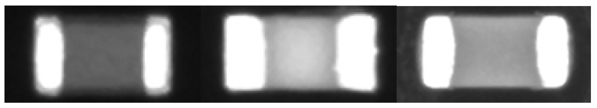
Figure 11.
Example of a component with excessive light balance, illustrating the importance of light balance detection in pre-processing.
Figure 11.
Example of a component with excessive light balance, illustrating the importance of light balance detection in pre-processing.

Figure 12.
Example of a blurry image captured during component inspection, emphasizing the need for effective detection and correction of blurry images in the pre-processing stage.
Figure 12.
Example of a blurry image captured during component inspection, emphasizing the need for effective detection and correction of blurry images in the pre-processing stage.


Figure 14.
SMT over edge high-level architecture diagram.

Figure 15.
The graphs show the Kubernetes cluster, based on Nvidia’s GPU, scaling to accommodate multiple production machines and growing production demands.
Figure 15.
The graphs show the Kubernetes cluster, based on Nvidia’s GPU, scaling to accommodate multiple production machines and growing production demands.

Figure 16.
The calculated dimensions of the components exemplifying the various components processed in the production line. Different colors in the chart represent different pick and place machines.
Figure 16.
The calculated dimensions of the components exemplifying the various components processed in the production line. Different colors in the chart represent different pick and place machines.

Figure 17.
(Top) processing time of the defects detection algorithm, (bottom) processing time of the corrosion detection algorithm, both running in parallel on the same images.
Figure 17.
(Top) processing time of the defects detection algorithm, (bottom) processing time of the corrosion detection algorithm, both running in parallel on the same images.


Table 1.
RPCA testing results.
| Component Type | Non-Defect Items Tested | Defect Items Tested | True Positive | True Negative | False Positive | False Negative | Accuracy | Recall |
|---|---|---|---|---|---|---|---|---|
| Capacitor | 610 | 51 | 19 | 527 | 83 | 32 | 0.826 | 0.373 |
| Resistor | 651 | 64 | 25 | 543 | 108 | 39 | 0.794 | 0.391 |
| SOT-23-3 | 1054 | 102 | 65 | 983 | 71 | 37 | 0.907 | 0.637 |
Table 2.
Evaluation of the presented model.
| Component Type | Non-Defect Items Tested | Defect Items Tested | True Positive | True Negative | False Positive | False Negative | Accuracy | Recall |
|---|---|---|---|---|---|---|---|---|
| Capacitor | 610 | 51 | 32 | 577 | 33 | 19 | 0.921 | 0.627 |
| Resistor | 651 | 64 | 40 | 628 | 23 | 24 | 0.934 | 0.625 |
| SOT-23-3 | 1054 | 102 | 72 | 1026 | 28 | 30 | 0.95 | 0.706 |
Table 3.
Algorithm and system performance of old architecture with new.
| Software Version | CPU | RAM (MB) | Throughput (c/s) |
|---|---|---|---|
| Edge (C++) | 0.1 | 25 | 460 |
| Edge (Py) | 0.14 | 123 | 4.6 |
Disclaimer/Publisher’s Note: The statements, opinions and data contained in all publications are solely those of the individual author(s) and contributor(s) and not of MDPI and/or the editor(s). MDPI and/or the editor(s) disclaim responsibility for any injury to people or property resulting from any ideas, methods, instructions or products referred to in the content. |
© 2024 by the authors. Licensee MDPI, Basel, Switzerland. This article is an open access article distributed under the terms and conditions of the Creative Commons Attribution (CC BY) license (https://creativecommons.org/licenses/by/4.0/).
Share and Cite
MDPI and ACS Style
Weiss, E.; Caplan, S.; Horn, K.; Sharabi, M. Real-Time Defect Detection in Electronic Components during Assembly through Deep Learning. Electronics 2024, 13, 1551. https://doi.org/10.3390/electronics13081551
AMA Style
Weiss E, Caplan S, Horn K, Sharabi M. Real-Time Defect Detection in Electronic Components during Assembly through Deep Learning. Electronics. 2024; 13(8):1551. https://doi.org/10.3390/electronics13081551
Chicago/Turabian StyleWeiss, Eyal, Shir Caplan, Kobi Horn, and Moshe Sharabi. 2024. "Real-Time Defect Detection in Electronic Components during Assembly through Deep Learning" Electronics 13, no. 8: 1551. https://doi.org/10.3390/electronics13081551
Note that from the first issue of 2016, this journal uses article numbers instead of page numbers. See further details here.