Article

A Power-Efficient High-Drive Current Mirror Combining a Regulated Cascode Topology with a Non-Linear CCII-Based Feedback

Microelectronics Department, Laboratory of Informatics, Robotics, and Microelectronics of Montpellier (LIRMM), UMR 5506, National Centre for Scientific Research (CNRS), University of Montpellier, 161 Rue Ada, CEDEX 5, 34095 Montpellier, France
*
Author to whom correspondence should be addressed.
Electronics 2024, 13(8), 1556; https://doi.org/10.3390/electronics13081556
Submission received: 5 February 2024 / Revised: 15 April 2024 / Accepted: 16 April 2024 / Published: 19 April 2024

Abstract

:
This brief presents a continuously regulated current mirror topology capable of providing a wide range of currents with high-precision and speed control features. The circuit combines a non-linear current-mode feedback solution for fast and energy-efficient operation with an input-referred regulated-cascode configuration for precise current mirroring. The proposed implementation has an output current ranging from 100 μ A to 2 mA , exhibits a fast response time of ≈100 ns for the full range steps, while ensuring a high power efficiency (>90%) and low current copy errors (<0.5%).

1. Introduction

Processing, amplifying or conveying current signals typically requires both static and dynamic current mirrors. Several performances are shared by both types, but it is clear that dynamic operation brings many more difficulties. Optimizing static and dynamic performances at once leads to conflicting decisions.
Several studies have demonstrated that the relation between static and dynamic performances is bounded by technological constants [1,2]. This specificity is referred to as the speed–power–accuracy trade-off. To quantify the role played by the technology in the design of a dynamic current mirror, the authors in [3] propose a figure-of-merits (1). It combines the bandwidth, the power consumption, and the relative accuracy of the current mirror.
Power Bandwidth × Accuracy 2 C OX A VTH 2 V DD g m I IN
where C OX is the gate oxide capacitance, A VTH is the process-dependent matching parameter related to the MOS threshold voltage V TH , g m is the transconductance factor of mirroring devices, and I IN is the input current. The above relation is an illustration of the fact that the global speed–power–accuracy performance does not depend on the size and bias of its devices. In other words, maximizing one of these three performances necessarily implies a cutback to the other. For a certain range of application, for instance whenever high-drive, high-speed or high-accuracy capabilities are required, the limit set by the technology makes it impossible to achieve the target performances.
More advanced current-mirror structures have a large variety, and the literature proposes numerous effective alternative topologies to improve the performances of classical current mirrors [4]. An observation would be that a limited number of published topologies precisely address the issues related to the speed–power–accuracy trade-off, despite the fact that this trade-off has been frequently studied and is unavoidably encountered in dynamic CMOS current-mirror design.
Using an analysis similar to [3], it can be proven that active-input current-mirror topologies (i.e., feedback between input node and gate voltage in Figure 1a) can improve the speed–power ratio with minimal impact on the overall accuracy. Published in [5] in an early version and lately deployed in various applications [6,7], such structures can overcome under certain conditions the technological limit as long as the power consumption of the feedback circuit can be kept moderately low compared to the current-mirror bias itself.
In a previous study [8], we have proven that the replacement of the voltage-mode feedback that exists in a standard active-input current mirror by a current-mode circuit (Figure 1b) significantly enlarges the stability domain and increases the maximum speed reachable while offering a supplementary degree of freedom to tune the system response. Unlike transconductance or voltage amplifiers, current-mode circuits are components with low-input impedance capable of absorbing current with minimal variation in their input voltage. It improves the current-mirror input compliance and pushes the input pole towards higher frequencies for a wider stability domain. In Figure 1b, the terms C I N and R I N denote the equivalent input capacitance and resistance, respectively; while these parameters are influenced by transistor characteristics, they are also influenced by the feedback circuit itself and any parasitic elements present at these nodes. The designation “i=0” signifies that due to the extremely low input impedance of the current-mode feedback circuit, there is minimal change in the input voltage V I N (i.e., “cste”). Consequently, no voltage variation across the equivalent input impedance ( C I N // R I N ) results in a negligible current flow through it.
It has been demonstrated in [8] that by forcing the current-mode feedback to have a non-linear behavior, static specifications can be unbidden from dynamic behavior for a much more power-efficient operation. For instance, thanks to the use of the proposed non-linear current-mode feedback, the speed of a standard diode-connected current mirror has been multiplied by 12.5 , while the static power consumed has only increased by a factor 1.4 , all with almost no impact on the initial current-copy accuracy or the system stability.
To go further, in this paper, we propose a continuously regulated topology which offers, by means of a second control loop, larger output impedance and better accuracy over wider current ranges, while it still preserves all the benefits of the original non-linear current-mode feedback. Simulation results and a state-of-the art comparison support the use of this topology as a competitive elementary current source for the design of high-performances circuits, capable of providing a wide range of currents (from several dozen μ A to several mA) with high-precision along with a high speed/power ratio.

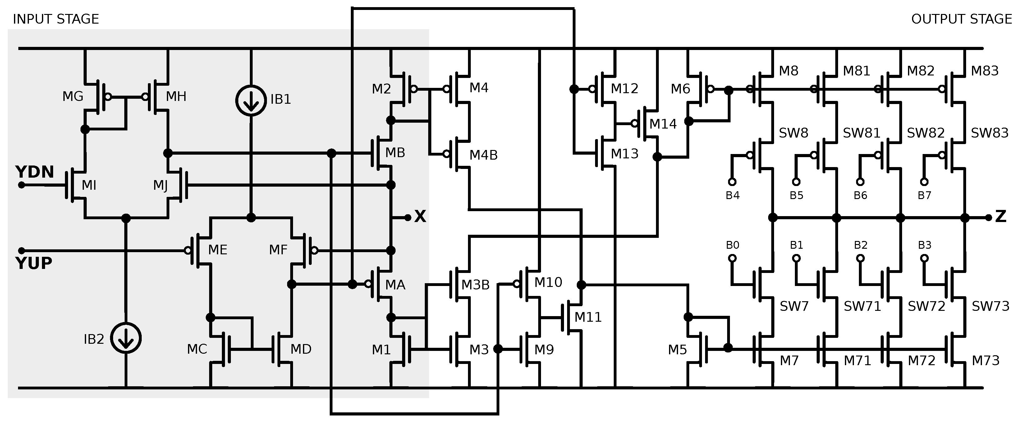
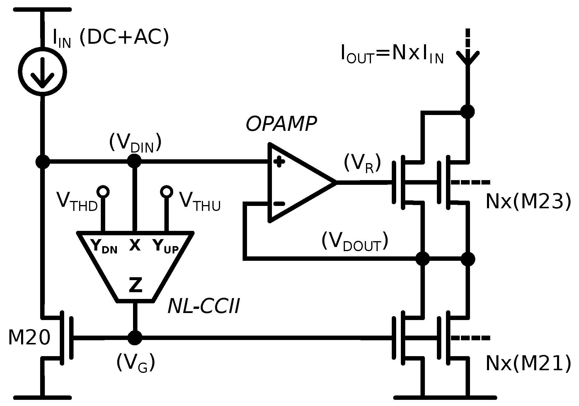
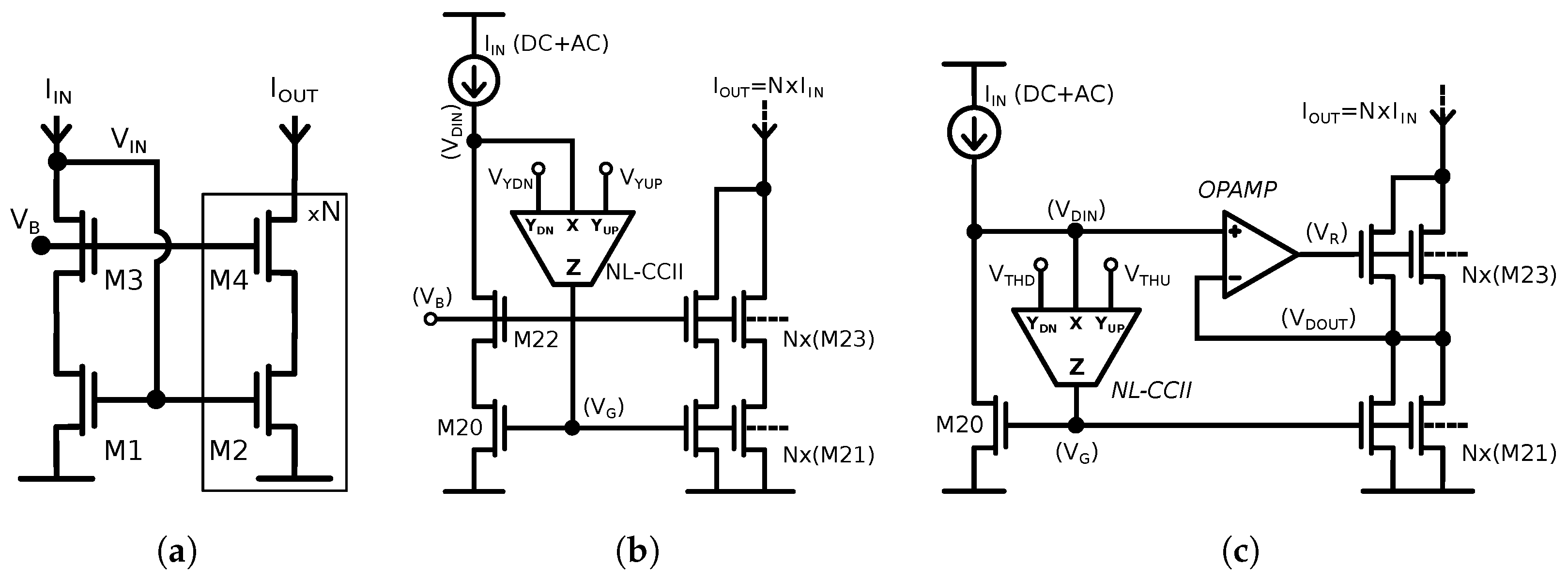
2. Improved Current Mirror with Non-Linear CCII-Based Feedback

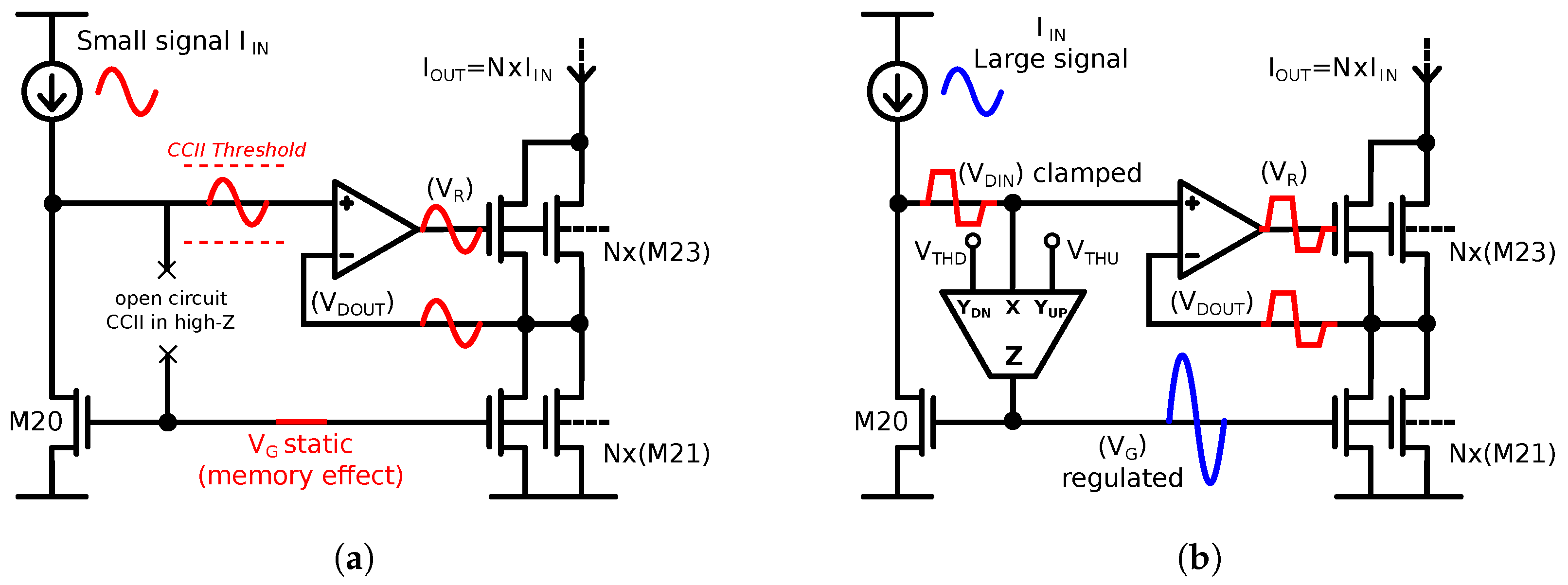
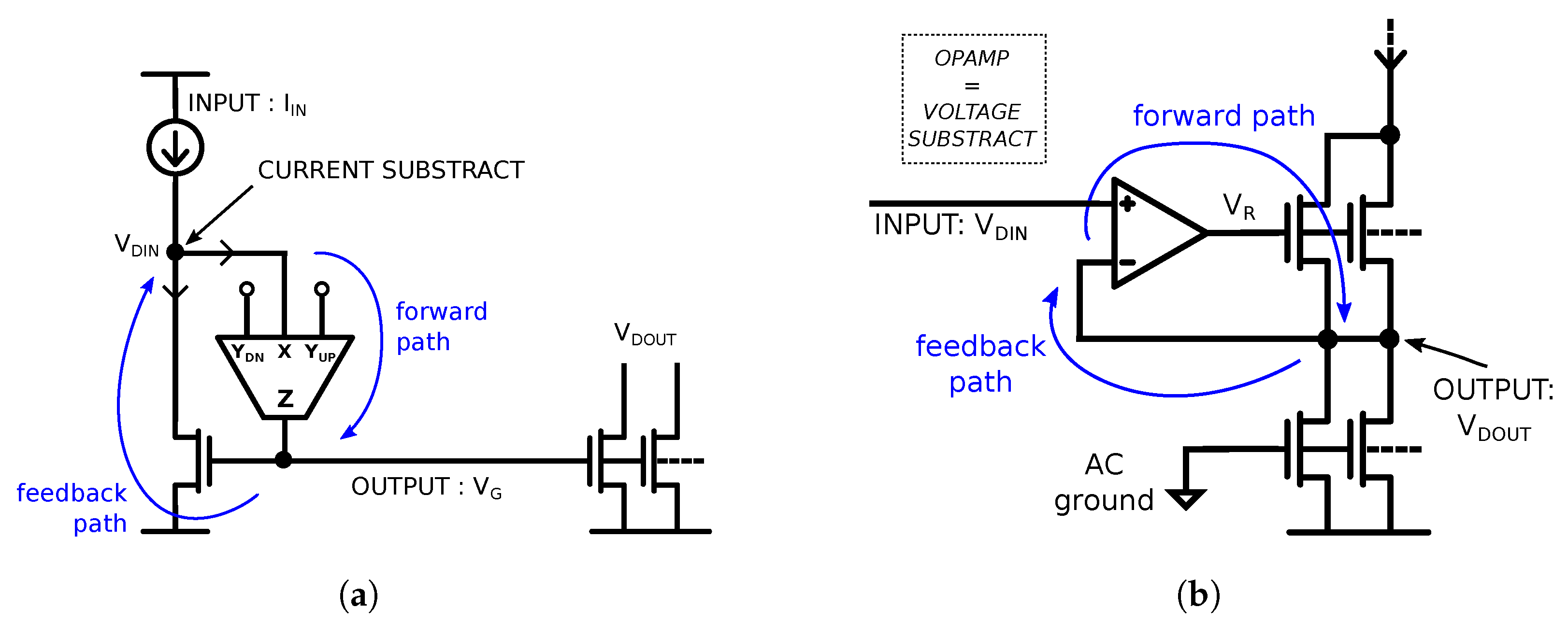
2.1. Principles of Operation

Illustrated in Figure 2, the proposed current-mirror topology relies on a gate voltage regulation using non-linear current conveyors (NL-CCII), in combination with an input-referred output-regulated cascode structure (IRRC), with a reference voltage terminal connected to the input node. This way, it forces the V DS equality of the mirroring devices, boosts the output impedance by the operational amplifier (OPAMP) gain and decreases the intrinsic input branch impedance compared to a classic or high-swing cascode structure which improve the input dynamic range. The originality of this improved topology is the two feedback loops operating simultaneously, regulating both the gate voltage for speed improvement and drain voltages for a precise current copy.
The accuracy of the current mirror is ensured conjointly by (i) large areas for the mirroring devices to minimize mismatch errors, (ii) drain regulation to reduce systematic errors due to asymmetrical v ds modulation in the mirroring pair, (iii) very high output impedance offered by the output regulated cascode configuration, and (iv) an impedance switching mechanism in the CCII that avoids the speed control loop to introduce static error on the output current.
The low power consumption is achieved thanks to (i) the use of low-power topologies for the OPAMP, (ii) the channel length of cascode devices sized close to the minimal dimension which reduces the capacitive load that the OPAMP has to drive, reducing consequently the bias current it requires, (iii) a large current gain or copy ratio for the current mirror to minimize current losses, and (iv) an unbiased non-linear CCII structure that consumes zero power in a steady state. For more details, see Section 2.3.
The dynamic behavior depends on the amplitude of the currents involved and differentiates in two cases: (i) For a small input error current ( I ϵ ), only the OPAMP is active (Figure 3a). The induced variation in the input voltage occurs within the range fixed by the two CCII thresholds. Equality between the input current and output current is achieved by modulation of the drain voltage of M 21 . The CCII stays in a high-impedance state, and the gate voltage is constant. The speed is mainly determined by the pole in the OPAMP output. (ii) For a large input current, the input voltage will reach one of the threshold values. The CCII is activated (Figure 2), and its low input impedance forces the input voltage to be clamped close to the threshold. Gate regulation is activated, and the output current follows the input variations according to gate voltage changes. The OPAMP is still active but in this case, the mirror speed is mainly dictated by the speed of the CCII-based control loop. Figure 3 summarizes both the small-signal and large-signal dynamic operation.
This improved structure also offers the possibility for the mirroring devices to operate in the triode region for a very high input-current range. According to the MOS current law in this operating region, we note that with the control of both drain and gate voltages, we are still capable of ensuring an accurate current copy. Highest values for the input current are principally determined by the residual DC offset and output common mode ranges ( O C M R ) of the OPAMP. Technically, with the NL-CCII structure and with mirroring devices operating in the triode region at a high current level, the gate voltage can go up to values close to the power supply. However, with the input current increasing and the mirroring devices going deeper in the triode region, we can observe a drastic reduction in their output impedance. For drain current modulation due to loads, this output impedance reduction is compensated by the high gain of the output-regulated cascode technique as long as the cascoded devices stay saturated.

2.2. System Model

The dynamic behaviour is determined by two feedback loops as depicted in Figure 4. Because they affect weakly dependent quantities and address two different characteristics of the current mirror, they can be treated separately. For the gate-voltage regulation based on such a non-linear current-mode feedback, a theoretical analysis of the dynamic behavior has been proposed in a previous author’s publication [8]. The general behavior of classic wide-swing or regulated cascode current mirrors, among others, has been covered in [9]. However, for the sake of clarity, we recall here the main elements.
The first feedback loop, based on the proposed non-linear CCII is dedicated to the speed control of the current mirror (Figure 4a). We are interested in the dynamic performances during a transient phase; the non-linear CCII is expected to be predominantly active, and the system dynamic will be treated without considering the high input impedance state. The block diagram in Figure 5 is derived from a small signal representation of the system shown in Figure 2. I ϵ corresponds to the difference between the reference current I I N and the current I M O S absorbed by the transistor at a given moment. A certain amount of I ϵ is driven by the CCII, the rest charges/discharges the parasitic capacitance on the input node under the voltage V D developed across the overall input conductance g I N ( V D ) . Parameters β , g Z and g X ( V D ) are, respectively, the gain, the output conductance and the input conductance of the CCII. Here, the CCII input conductance depends on the input voltage. τ X ( V D ) , τ Z and τ C C represent, respectively, the time constant on the input drain, the time constant on the current mirror gates and the intrinsic time constant of the CCII ( τ = g m / C ). The current I Z represents the current flowing through the CCII output node Z, and the voltage V G is the voltage across the gate of the current mirror formed by transistors M20 and M21.
The block with input I Z and output V G in Figure 5 represents the process where the current from the CCII’s output node Z is converted into a voltage across the gate capacitance of transistors M20 and M21. As a simplified approximation, the time constant τ Z can be considered as g Z divided by the parallel combination of C G S 20 and C G S 21 , which forms the basis of the near-perfect integrator function. Assuming that the input time constant is negligible compared to the time constant on the gates of the current mirror M20–M21, in short τ X < < τ Z , an approximated expression for the closed-loop transfer function is derived in (2).
H C L = β g Z + β g m 20 1 1 + g Z τ Z τ C C g Z + β g m 20 s + g Z ( τ Z τ C C ) g Z + β g m 20 s 2
with the natural pulsation
ω n = g Z + β g m 20 g Z τ Z τ C C β ω C C ω C M
Characteristics of the step response can be estimated using classical relations between the frequency domain and time domain behaviors. For instance, for an under-damped second-order system ( m < 0.7 ) in the form of (2), overshoot O V and response time at n % ( t r n % ) are approximated by the following expression:
t r n % = 1 m ω n ln 100 n O V % = 100 e π m 1 m 2
The second feedback loop is made for high accuracy and high output impedance. It can bee seen as a low-output-impedance voltage amplifier, with unity gain feedback, loaded by a resistance ( r DS of M21). Here, we consider that the dominant capacitance is the gate capacitance of M23, and thus, the dominant pole is on the OPAMP output. Drain-to-source capacitance of M21 and input capacitance of the OPAMP are neglected. The amplifier DC offset is included as a voltage source in series with the non-inverting OPAMP input. The block diagram used for the analysis is shown in Figure 6. The parameter A 0 is the open-loop gain of the OPAMP, and the parameter G B W is its gain-bandwidth product. The equivalent conductance g DSeq is defined as g DSeq = g DS 21 / / g DS 23 .
The voltage transfer function V DOUT / V DIN for drain regulation of the mirroring devices is given in (5). We observe that the speed of this loop is dominated by the intrinsic speed of the cascode device M23, which support the decision to size cascode devices with minimal channel length for a small gate capacitance and a high transconductance gain.
V DOUT V DIN = G CL 1 + τ 2 s 1 + τ 1 s = A 0 1 + A 0 2 π G B W s × 1 + τ 2 s 1 + τ 1 s
τ 2 = C GS 23 g m 23 τ 1 = C GS 23 g m 23 + g DSeq
The expression of the total output impedance seen by the load is displayed in (7). The higher the OPAMP open-loop gain A 0 , the higher the output impedance, and the closer the voltage transfer gain is to the unity gain.
r OUTCM = r DS 21 + r DS 23 + A 0 × g m 23 × r DS 21 × r DS 23
However, the frequency behavior affects in the same proportion the input voltage V DIN and the OPAMP offset voltage V OFF . Hence, the totality of static voltage errors in the OPAMP is reported to the drain voltage of M23 and generates an output current error I OFF = g DS 21 × V OFF . However, with an offset in the order of 10 mV and an output impedance value for the mirror device of about 1 M Ω , this error current is found to be in the order of the dozen of nA . In the triode region, the output impedance can go down to several k Ω , significantly increasing the error current, but it occurs at large output currents. The relative difference has to be examined to see if the error due to the OPAMP offset starts to dominate the overall error.

2.3. Design Considerations for the NL-CCII and the OPAMP

A schematic of the NL-CCII is presented in Figure 7. This implementation uses self-biased cascoded devices (M3B and M4B) to improve gain linearity and save voltage headroom for a wider current dynamic. The output stage is composed of configurable output current mirrors for a digital control (B0-B7) of the NL-CCII current gain values. Nodes B0–B7 are digital nodes controlled externally, typically by a digital core that will manage the current source. These control bits allow for the tuning of the NL-CCII gain and thus the resulting speed of the system. They can be used to fine-tune the system response or to save power by reducing the NL-CCII gain in applications where fast current waves are not always demanded. Sizes of transistors composing the NL-CCII are given in Table 1.
The OPAMP used for the V DS control loop is identical to the OPAMP controlling the transistor MB in the CCII input stage. Differential pairs are biased in moderate inversion under a tail current of 5 μ A (IB1 and IB2) and are realized with low V TH devices. To restrict the static consumption to a minimum, while ensuring sufficient output compliance, we opted for a single-stage amplifier with no cascode configuration. More advanced OPAMP topology can replace the single-stage OPAMP in both drain and gate feedback but with a certain increase in the power budget, which is not always justifiable. Techniques that reduce the OPAMP DC offset will also reduce the copy error at a high current level. Techniques that increase its gain-bandwidth product will lead to a higher output impedance when used for drain regulation and sharper transition between the two NL-CCII states when used for gate regulation.
The CCII input impedance value depends on the operating regions of MA, MB, M1 and M2, which relate to the input voltage V D through the comparators. In the high-impedance state, MA and MB are OFF, and the CCII input impedance can be approximated by
r X h z r O F F M A / / r O F F M B for V Y D N < V D < V Y U P
In the low-impedance state, either MA or MB is ON, and the input impedance expresses as
r X l z r O N M A + 1 / g m M 1 for V D > V Y U P r X l z r O N M B + 1 / g m M 2 for V D < V Y D N
To achieve a better stability margin and better speed, we want to minimize the r X value for the low impedance state. This is carried out using a large channel width for the switches MA and MB and a large W/L ratio for M1 and M2. Transistors M1 and M2 can be sized to be in weak inversion for low levels of CCII input current, maximizing their transconductance and consequently the input current dynamic. Because there is no static biasing for these current mirrors, the CCII might show significant gain distortion and cut-off frequency variation across the full current dynamic, which can lead to detuned feedback. To limit these effects in the proposed implementation, high-impedance self-biased cascode current mirrors have been used in place of the simple current mirrors M1–M3 and M2–M4. Eventually, to enforce the switching mechanism, the output node is also quickly turned into high impedance using switches controlled by the same signal used for the input. Ensuring that the current stops flowing out of the CCII at the same time, the input stage goes from the low to high impedance state. The duration of the output stage to switch between the high and low impedance state mainly depends on the delay of the inverters M9–M10 and M12–M13 and on current capabilities of the shorting devices M11 and M14.
There are few constraints on the voltage copy error from nodes Y to node X and on the current copy errors from node X to node Z. The voltage copy ensures that voltage at node X is always within the two threshold values; no precision is required here. As for the current copy, because we are dealing with a closed-loop system with integral action, CCII current-copy errors are compensated by the control loop. Therefore, the design constraint of the CCII internal current mirrors can be relaxed.

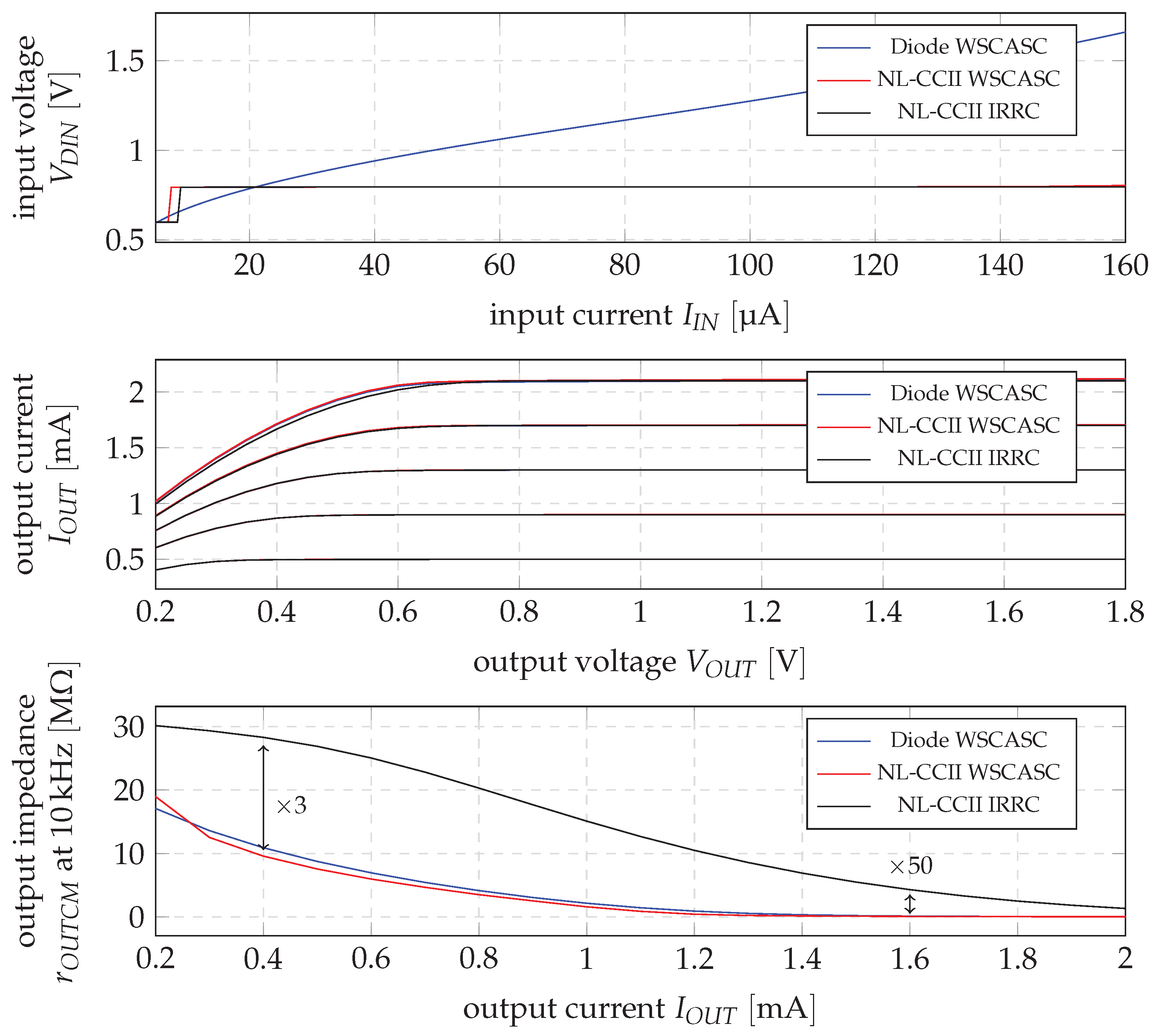
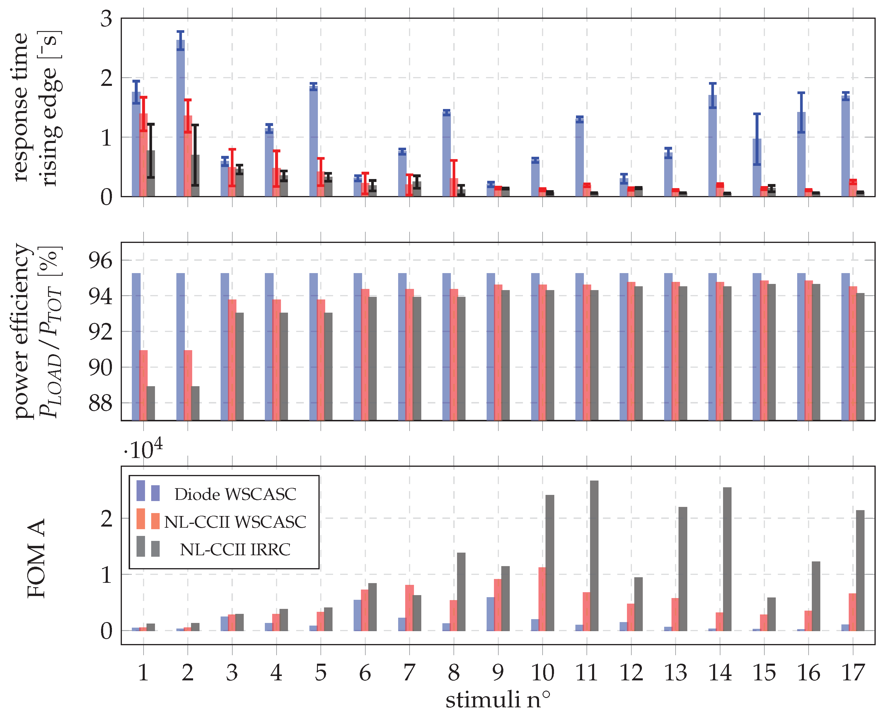
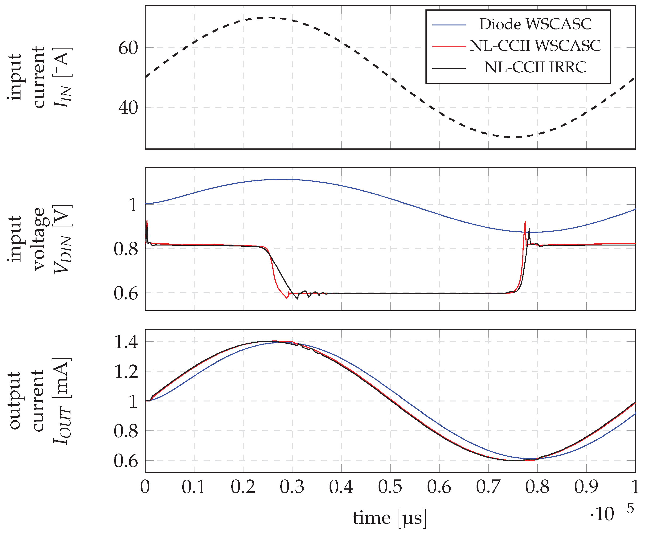
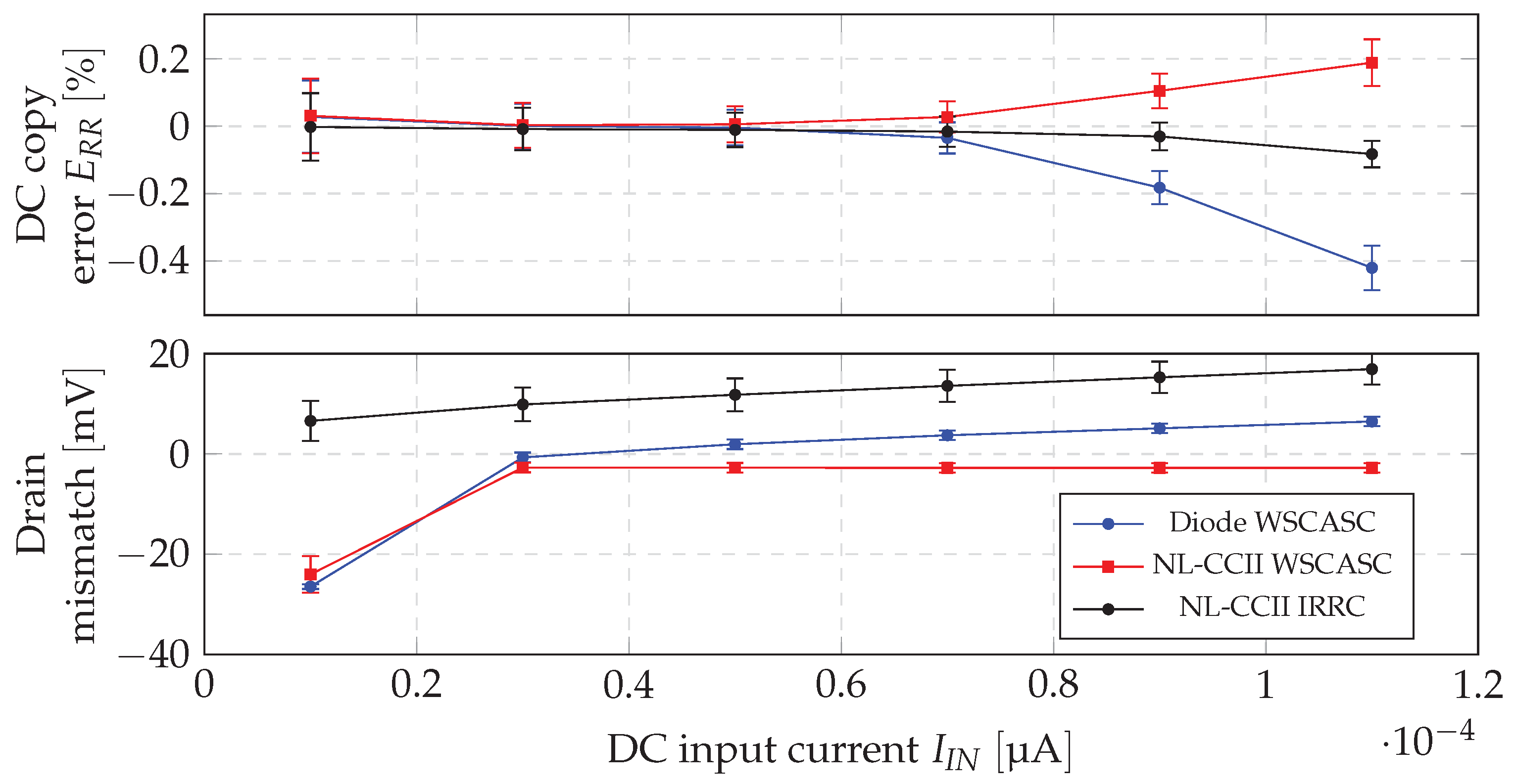
3. Simulation Results and Comparison with Reference Structures

To validate the previous assessments, here, we present simulation results of an implementation of the improved input-referred output-regulated cascode current mirror with non-linear CCII-based feedback (Figure 8c). For comparison purposes, we have also implemented the equivalent high-swing cascode current mirrors with both diode-connection (Figure 8a) and non-linear CCII-based feedback (Figure 8b).
The circuits have been designed using the TSMC 0.18 μ m standard CMOS process and operate at 1.8 V. In the whole following characterization, the mirroring devices of the three current mirrors presented in Figure 8 are sized with W CM / L CM = 21.5   μ m / 18   μ m and cascode devices with W CM / L CM = 21.5   μ m / 0.25   μ m , in order to operate on the edge of the strong inversion at the minimum input current I IN = 5 μ A . The mirror current gain (or copy ratio) is fixed at N = 20 , leading to a minimum output current of 100 μ A . CCII thresholds are here fixed at 0.6   V and 0.8   V in the NL-CCII IRRC CM for compatibility with test resources that we used but did not address in this publication.
Simulation benches are the following: (i) A measure of the influence of the channel length on the accuracy and bandwidth for the diode-connected current mirror. We look at the speed versus the variability for a small dimension as well as for the maximum dimension authorized by the process rules. (ii) A measure of static performances such as input/output compliances, systematic current transfer errors (no mismatch) and output impedances. (iii) An illustration of the typical dynamic behavior with measurement of the step response and the harmonic response for a full-range input signal. (iv) Statistical measurements to evaluate both static and dynamic performance dispersions.

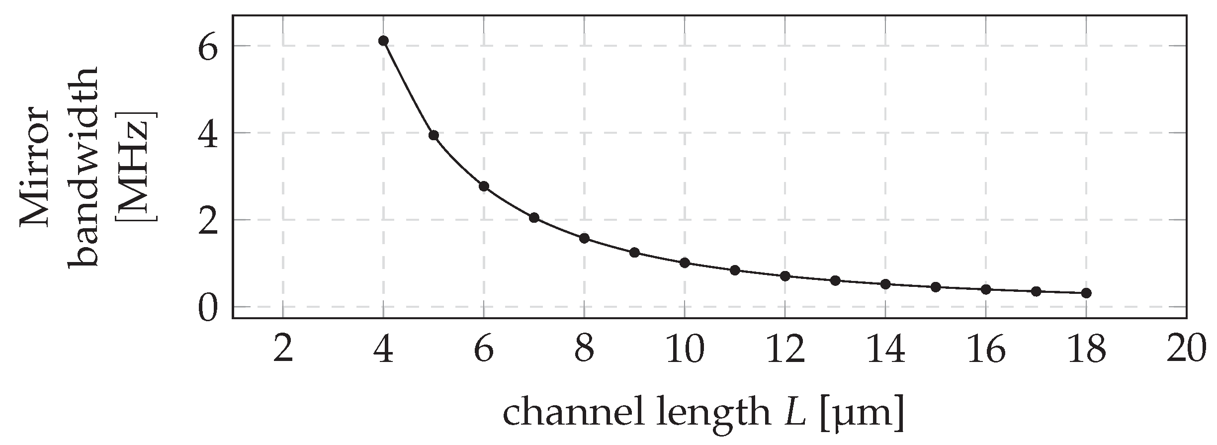
3.1. CM Sizing and Speed–Accuracy Trade-Off

In this first test, we compare the accuracy and bandwidth of a diode-connected high-swing cascode current mirror (Figure 8a) for a channel length ( L CM ) ranging from 4 μ m to 18 μ m (the maximum length allowed by the DRC rules). The operating point is fixed at I IN = 30   μ A (current source), V out = V DD / 2 = 0.9   V (voltage source) and V B = 1.3   V (voltage source). The (W/L) ratio of mirroring devices is kept constant and chosen such that V IN 0.9   V for the considered operating point ( W CM / L CM = 1.2 ). The channel width of cascode devices W CASC are kept equal to the width of mirroring devices W CM . Lengths L CASC are taken at the fixed value of 0.25 μ m . Figure 9 shows the DC output error distribution for different channel lengths, taking into account systematic errors, process variations and mismatch errors. Figure 10 is an AC measurement of the current-mirror bandwidth as a function of the channel length L CM .
As expected, the output error and bandwidth both decrease when the channel length increases. This means that by taking the mirror devices with the maximum length (18 μ A ), we have spent all of the speed–accuracy budget to minimize the output error [3]. This will be our choice for the next tests. The NL-CCII of the gate-voltage control loop is in charge of speeding up the mirror with minimal impact on error and power.

3.2. Typical Static and Dynamic Behaviour

By looking at static behaviors given in Figure 11, we compare input/output compliances and output impedances. We observe that while all the circuits require approximately the same minimum output voltage for a proper operation in the saturated region ( V OUT > 0.7   V for I OUT up to 2 mA ), the minimum input requirement is drastically different between the diode-connected configuration and the one with NL-CCII-based feedback. Thanks to the input switching mechanism of the CCII, the input voltage is constrained, and the minimum admissible value is actually equal to the upper threshold value ( 0.8   V ). For the considered device sizes, the diode-connected high-swing cascode mirror shows a lower input requirement as long as the input current is under 20 μ A . However, the minimum admissible value increases with the input current at a rate of I IN , which significantly reduces the room for the input source to operate at a high current level. In parallel, we observe one of the main advantages of the regulated cascode topology by looking at the output impedance, which shows an increase ranging from × 3 to × 50 when compared to the two other equivalent current mirrors.
We now consider the dynamic behavior of each of the three circuits illustrated by a transient simulation with a full-range signal applied to the input. For time domain evaluation, the input stimuli is a 3 μ s current pulse from 5 μ A to 100 μ A which leads to an output current pulse of 100 μ A to 2 m A . For the distortion performance, we looked at the output current spectrum when the input stimuli is a pure sine wave of 50   μ A ± 20   μ A at 100 kHz . Observed response times at 0.4 % (Table 2) demonstrate the efficiency of the NL-CCII-based feedback to speed up the current mirror at a minimal power cost.
Regarding the distortion simulations (Table 3), the NL-CCII IRRC shows better THD ( 44 dB) and SFDR (46 dB) for the step considered thanks to the drain regulation and the high output impedance offered by the topology. For the same step, the DCO WSCASC mirror, taken as a reference, exhibits a THD of 28 dB and an SFDR of 30 dB. However, when the step amplitude decreases, the effects of noise and distortion generated by the CCII switching mechanism become more important and degrade the THD. The diode-connected configuration generally shows a greater linear response for small signal inputs. Figure 12 shows the results of the long-time transient simulation for which we have calculated the spectrum and measured the THD and SFDR.

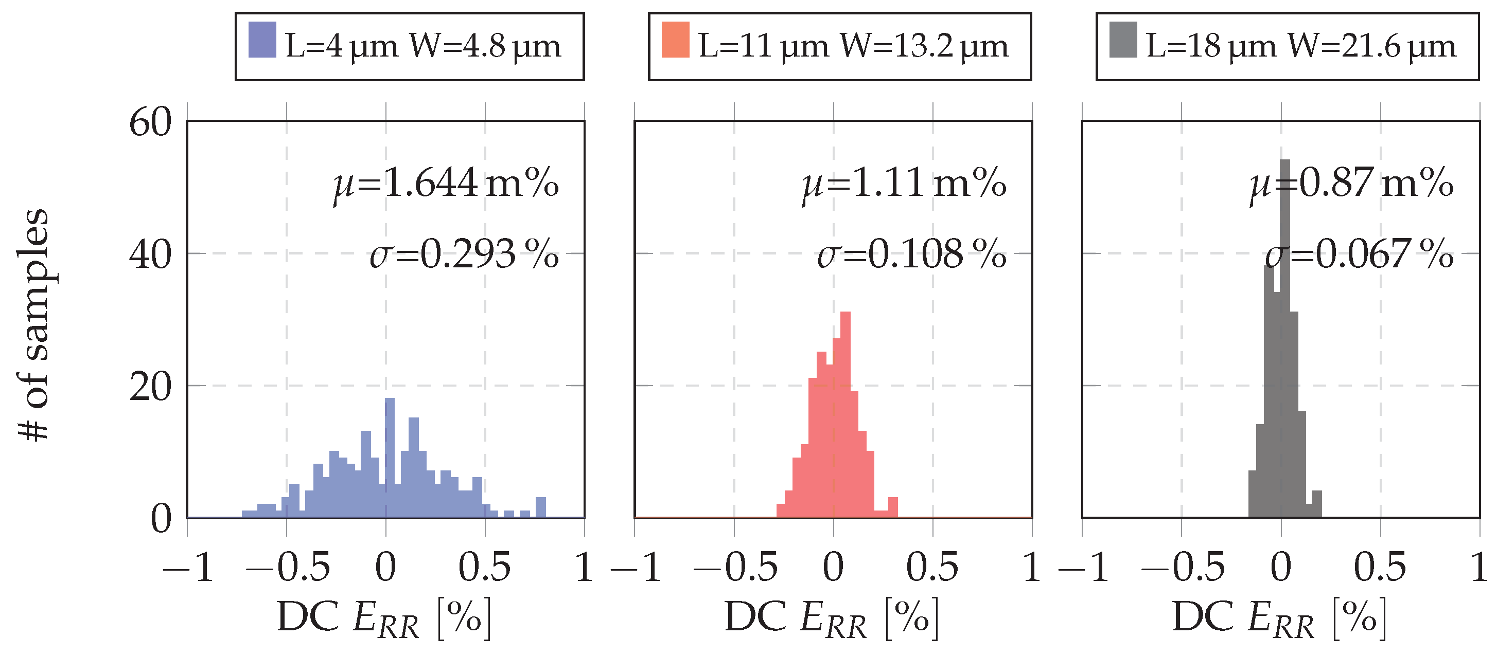
3.3. Statistical Results and Speed-Power-Accuracy Metrics

Monte-Carlo simulations are performed for statistical evaluations of the overall copy error, the drain mismatch of mirroring devices (absolute difference between drain voltages) and the settling time. The three circuits are stimulated with several steps of various amplitudes, ranging from ± 500   n A to ± 55   μ A while biased at different levels across the input current range, starting from 10 μ A up to 110 μ A . Stimuli cases are summarized in Table 4.
To evaluate the speed–power–accuracy metrics, the following definitions will be employed: The response time t r 0.4 % will be assessed based on the transient response. The static output error E R R is determined by summing the systematic and random errors as follows:
DC copy error = | μ ( E R R ) | + | σ ( E R R ) |
Power efficiency is defined as the ratio of the power delivered to the load ( I O U T × V D D ) to the total power dissipated, including input reference currents and dedicated bias for the feedback circuits:
power efficiency = P L O A D P T O T = I O U T I O U T + I I N + I B I A S
The bandwidth is estimated as
estim . bandwidth = 1 2 π × τ 1 2 π × t r 0.4 % 5
The static output error and drain mismatch versus input current range characteristics are reported in Figure 13. The curve represents the average values, and error bars show the corresponding standard deviation ( ± σ ). Figure 14 puts in relation the observed response time and its standard deviation with the static power efficiency for each of the 17 stimuli cases. As expected, the NL-CCII IRRC CM exhibits a drain-voltage difference (10–20 mV ) slightly greater than the WSCASC configurations (5–10 mV ), but looking at the copy error plot, we observe that the NL-CCII IRRC CM still offers the highest accuracy, and the error at 1 σ is always lower than 0.2% for the full input range. Regarding the mirror speeds (Figure 14), we observe larger relative standard deviations (error bars) for both topologies based on the current conveyor. This is explained by the device dimensions constituting the CCII. Transistors are all close to minimal dimensions to reduce the silicon area and achieve a high-speed feedback operation but at the price of large variability. The absolute amount of response time dispersion is a small percentage of the speed which has itself decreased from several μ s to hundreds of ns , making this amount almost insignificant.

4. Discussion and Conclusions

In order to quantify the improvements regarding the speed–power–accuracy trade-off, we propose the two generic metrics (FOM A and FOM B) given below.
FOM A = power eff / ( resp . time × dc error )
FOM B = power eff × bandwidth / dc error
As shown in Figure 14, in comparison with the equivalent DCO WSCASC and NL-CCII WSCASC current mirrors, the proposed topology exhibits the best score on the FOM A for each simulated stimuli case.
To compare the NL-CCII IRRC CM with other topologies of the advanced current mirror available in the literature, we use the performances observed for the full-range stimuli case. The performance summary and scores for the FOMs are presented in Table 5. According to the scores achieved by the different circuits, the proposed NL-CCII IRRC CM is found to be one competitive structure to achieve a fast and precise response at minimal power while offering high dynamic and high drive capabilities.
Finally, this study demonstrates the advantages of our advanced current-mirror design approach which relies on the combination of a non-linear current mode feedback and drain-voltage regulation. This topology is particularly suitable for applications requiring simultaneously high-speed and high-drive capabilities (from μ A to mA in hundreds of ns) but also the maximum current-copy accuracy allowed by the technology.
There is a certain number of topics, not specifically treated in this paper, that may be worth citing to open the discussion on the outcomes: (i) The proposed non-linear current conveyor architecture is one of the successful candidates to implement the current-mode non-linear feedback control, but other solutions can be thought. For instance, very low-voltage applications may require a much simpler implementation with a limited number of devices. On the other hand, for applications with a higher power budget, we might opt for modified versions of high-drive or high-speed current conveyors/amplifiers that reuse the principle of the input impedance switching mechanism. (ii) To deploy this approach for current source architectures dealing with harmonic signals (sine waves, multi-tonal waves, …), the design effort on the feedback circuit should focus more on the linearity optimization than the optimization of the static precision. Requirements over the CCII specifications would slightly differ. (iii) The input impedance switching mechanism of the CCII, and the way it is used, presents some similarities with the work carried out in the past on current memory cells. A comment would be that some answers to the points raised above may be found with a deeper investigation of this domain.

Author Contributions

Conceptualization, M.J. and G.C.; Formal analysis, M.J., F.S. and G.C.; Investigation, M.J.; Methodology, M.J. and G.C.; Project administration, S.B. and G.C.; Supervision, S.B. and G.C.; Validation, M.J.; Visualization, M.J.; Writing—original draft, M.J.; Writing—review and editing, M.J., S.B., F.S., V.K. and G.C. All authors have read and agreed to the published version of the manuscript.

Funding

This research received no external funding.

Data Availability Statement

Data are contained within the article.

Conflicts of Interest

The authors declare no conflicts of interest.

References

  1. Kinget, P.R.; Steyaert, M. Impact of transistor mismatch on the speed-accuracy-power trade-off of analog CMOS circuits. In Proceedings of the Custom Integrated Circuits Conference, San Diego, CA, USA, 5–8 May 1996. [Google Scholar] [CrossRef]
  2. Bastos, J.; Steyaert, M.; Pergoot, A.; Sansen, W. Mismatch Characterization of Submicron MOS Transistors. Analog. Integr. Circuits Signal Process. 1997, 12, 95–106. [Google Scholar] [CrossRef]
  3. Kinget, P.R. Device mismatch and tradeoffs in the design of analog circuits. IEEE J. Solid-State Circuits 2005, 40, 1212–1224. [Google Scholar] [CrossRef]
  4. Aggarwal, B.; Gupta, M.; Gupta, A.K. A low voltage wide swing level shifted FVF based current mirror. In Proceedings of the 2013 International Conference on Advances in Computing, Communications and Informatics (ICACCI), Mysore, India, 22–25 August 2013. [Google Scholar] [CrossRef]
  5. Serrano, T.; Linares-Barranco, B. The active-input regulated-cascode current mirror. IEEE Trans. Circuits Syst. I Fundam. Theory Appl. 1994, 41, 464–467. [Google Scholar] [CrossRef]
  6. Moazzeni, S.; Cowan, G.E.R. Application of active current mirrors to improve the speed of analog decoder circuits. In Proceedings of the 2009 52nd IEEE International Midwest Symposium on Circuits and Systems, Cancun, Mexico, 2–5 August 2009. [Google Scholar] [CrossRef]
  7. Julien, M.; Bernard, S.; Soulier, F.; Kerzerho, V.; Cathebras, G. Formal analysis of high-performance stabilized active-input current mirror. In Proceedings of the 2017 IEEE International Symposium on Circuits and Systems (ISCAS), Baltimore, MD, USA, 28–31 May 2017. [Google Scholar] [CrossRef]
  8. Julien, M.; Bernard, S.; Soulier, F.; Kerzèrho, V.; Cathèbras, G. Breaking the speed-power-accuracy trade-off in current mirror with non-linear CCII feedback. Microelectron. J. 2019, 83, 77–85. [Google Scholar] [CrossRef]
  9. Aggarwal, B.; Gupta, M.; Gupta, A.K. A comparative study of various current mirror configurations: Topologies and characteristics. Microelectron. J. 2016, 53, 134–155. [Google Scholar] [CrossRef]
  10. Li, Y.; Wang, H.; Trik, M. Design and simulation of a new current mirror circuit with low power consumption and high performance and output impedance. Analog. Integr. Circuits Signal Process. 2024, 119, 29–41. [Google Scholar] [CrossRef]
  11. Xie, H.; Wang, Z.; Liu, G.; Lu, J.; Yi, X. A novel active-input cascode current mirror with high precision and low power dissipation. Eng. Rep. 2022, 4, e12451. [Google Scholar] [CrossRef]
  12. Pennisi, S. A low-voltage design approach for class AB current-mode circuits. IEEE Trans. Circuits Syst. II Analog. Digit. Signal Process. 2002, 49, 273–279. [Google Scholar] [CrossRef]
  13. Safari, L.; Minaei, S. A simple low voltage, high output impedance resistor based current mirror with extremely low input and output voltage requirements. In Proceedings of the 2016 39th International Conference on Telecommunications and Signal Processing (TSP), Vienna, Austria, 27–29 June 2016. [Google Scholar] [CrossRef]
  14. Vajpayee, P.; Srivastava, A.; Rajput, S.; Sharma, G. Low voltage regulated cascode current mirrors suitable for sub-1V operation. In Proceedings of the 2010 IEEE Asia Pacific Conference on Circuits and Systems, Kuala Lumpur, Malaysia, 6–9 December 2010. [Google Scholar] [CrossRef]
  15. Koliopoulos, C.; Psychalinos, C. A Comparative Study of the Performance of the Flipped Voltage Follower Based Low-Voltage Current Mirrors. In Proceedings of the 2007 International Symposium on Signals, Circuits and Systems, Iasi, Romania, 13–14 July 2007. [Google Scholar] [CrossRef]
Figure 1. (a) General active-input principle. (b) Equivalent current-mode version.
Electronics 13 01556 g001
Figure 2. Proposed input-referred regulated cascode current mirror (IRRC) with non-linear CCII-based feedback.
Electronics 13 01556 g002
Figure 3. Schematized operation of the improved structure. (a) Small signal operation. (b) Large signal operation.
Electronics 13 01556 g003
Figure 4. Concurrent closed-loop systems considered. (a) For V GS control. (b) For V DS control.
Electronics 13 01556 g004
Figure 5. Block diagram modeling the CCII-based feedback solution.
Electronics 13 01556 g005
Figure 6. Block diagram modeling the output drain voltage control loop.
Electronics 13 01556 g006
Figure 7. Implementation of the non-linear CCII with configurable current gain for both sink and source output current ( 2 × 4 bits).
Electronics 13 01556 g007
Figure 8. The three evaluated current mirror structures: (a) DCO WSCASC CM: diode-connected wide-swing cascode, (b) NL-CCII WSCASC CM: non-linear CCII-based wide-swing cascode, (c) NL-CCII IRRC CM: non-linear CCII-based input-referred regulated cascode.
Electronics 13 01556 g008
Figure 9. Static output error of the diode-connected wide-swing cascode current mirror (DCO WSCASC CM) at various lengths.
Electronics 13 01556 g009
Figure 10. Simulated bandwidth for the diode-connected wide-swing cascode current mirror (DCO WSCASC CM) at various lengths of the mirroring devices. As expected, the bandwidth is decreasing proportionally to 1 / L 2 .
Electronics 13 01556 g010
Figure 11. Static characteristics of input voltage versus input current, output I/V curve and output impedance versus output current. V B = 1.3   V . CCII thresholds = 0.6   V and 0.8   V .
Electronics 13 01556 g011
Figure 12. One period of a long time simulation with a harmonic signal. Input current wave has a DC component of 50 μ A and a magnitude of 20 μ A at 100 kHz .
Electronics 13 01556 g012
Figure 13. DC current copy error and drain mismatch of mirroring device.
Electronics 13 01556 g013
Figure 14. Response time at 0.4 % with error bars representing the standard deviation, power efficiency and evaluation of the FOM A, for each stimuli reported in Table 4.
Electronics 13 01556 g014
Table 1. Transistors sizing for the NL-CCII.
W/L W/L W/L W/L
μ m μ m μ m μ m
M1 3.5 / 0.25 M2 5 / 0.25 M5 0.45 / 0.25 M6 1.5 / 0.25
M3 3.5 / 0.25 M4 5 / 0.25 M7 2 × 0.45 / 0.25 M8 2 × 1.5 / 0.25
M3B 12 / 0.25 M4B 20 / 0.18 M71 4 × 0.45 / 0.25 M81 4 × 1.5 / 0.25
MA 7 / 0.18 MB 2 / 0.18 M72 8 × 0.45 / 0.25 M82 8 × 1.5 / 0.25
MC 1 / 1.5 MG 0.5 / 1.5 M73 12 × 0.45 / 0.25 M83 12 × 1.5 / 0.25
MD 1 / 1.5 MH 0.5 / 1.5 M9 0.5 / 4.5 M12 0.5 / 4.5
ME 2.5 / 0.5 MI 2 / 0.5 M10 2.5 / 4.5 M13 2.5 / 4.5
MF 2.5 / 0.5 MJ 2 / 0.5 M11 0.5 / 4.5 M14 2.5 / 4.5
Transistors ME, MF, MI and MJ are low-threshold devices.
Table 2. Response time ( t r 0.4 % ) and static power efficiency ( P W EFF ) for a full range input signal.
tr 0.4 % PW EFF at PW EFF at
I OUT = 100   μ A I OUT = 2   mA
DCO WSCASC CM 1.69   μ s 95.2 % 95.2 %
NL-CCII WSCASC CM244 n s 90.9 % 94.5 %
NL-CCII IRRC CM 71.4   n s 88.9 % 94.1 %
Table 3. THD and SFDR measurements for a sine wave of 50   μ A ± 20   μ A at 100 kHz .
THD (dB)SFDR (dB)
DCO WSCASC CM−27.830.2
NL-CCII WSCASC CM−35.437.24
NL-CCII IRRC CM−43.746.32
Table 4. Stimuli summary.
#BiasStep#BiasStep
110 μ A ± 0.5   μ A 970 μ A ± 0.5   μ A
210 μ A ±2 μ A 1070 μ A ±2 μ A
330 μ A ± 0.5   μ A 1170 μ A ±20 μ A
430 μ A ±2 μ A 1290 μ A ± 0.5   μ A
530 μ A ±20 μ A 1390 μ A ±2 μ A
650 μ A ± 0.5   μ A 1490 μ A ±20 μ A
750 μ A ±2 μ A 15110 μ A ± 0.5   μ A
850 μ A ±20 μ A 16110 μ A ±2 μ A
1760 μ A ±55 μ A
Table 5. Performance summary and comparison with previous published work.
PerfThis Work[10][11][12][13][9][14][15]
Technology ( μ m )0.180.180.180.50.180.180.250.18
Supply voltage ( V )1.81110.91.811.5
Min output current ( μ A )100500.110000
Max output current ( μ A )20001000100010060280300
Output error (%)0.0620.160.40.30.852.4
Resp. time at 1% ( μ s )0.070.04 0.07 0.02
THD (%) FR = Full Range0.65 @ 36% FR 0.8 @ 50% FR0.8 @ 50% FR 1
Bandwidth (MHz)11.151688214080132398
Power efficiency (%)94.12505030 503340
FOM A22.70.63 1.07 0.33
FOM B17.54.225.610.5 8.252.633.08
Disclaimer/Publisher’s Note: The statements, opinions and data contained in all publications are solely those of the individual author(s) and contributor(s) and not of MDPI and/or the editor(s). MDPI and/or the editor(s) disclaim responsibility for any injury to people or property resulting from any ideas, methods, instructions or products referred to in the content.

