
A P/X Dual-Band Co-Aperture Array with Dual-Polarized Antenna Based on Forest Biomass Measurement Applications

1
Aerospace Information Research Institute, Chinese Academy of Sciences, Beijing 100190, China
2
School of Electronic, Electrical and Communication Engineering, University of Chinese Academy of Sciences, Beijing 100039, China
3
School of Electronic Information and Electrical Engineering, Shanghai Jiao Tong University, Shanghai 200240, China
*
Author to whom correspondence should be addressed.
Electronics 2024, 13(8), 1565; https://doi.org/10.3390/electronics13081565
Submission received: 11 March 2024
/
Revised: 15 April 2024
/
Accepted: 18 April 2024
/
Published: 19 April 2024
(This article belongs to the Special Issue RF/Microwave Device and Circuit Integration Technology)
Abstract
:In this paper, a co-aperture dual-polarized antenna array is proposed. The frequency band covers the P-band (0.4–0.7 GHz) and the X-band (9.3–9.9 GHz). The P-band array is designed in the form of an all-metal Vivaldi, while minimizing the impact of the P-band antenna array structure on the X-band electrical performance. The final profile design for the dual-band antenna structure is only 0.12 λ0 (λ0 corresponds to the wavelength of 0.4 GHz). The X-band design adopts the miniaturized waveguide slot structure, which can be well embedded in the P-band array structure. In order to verify the feasibility of the scheme, prototype processing and testing were carried out, and the test results are consistent with the simulation results. The active VSWRs of the overall design are less than 2.0. Additionally, the dual-band antenna array has favorable radiation performance in each frequency band. It can be used in forest biomass measurements and other interferometric applications.
1. Introduction
Forest biomass refers to the total weight of all living organisms that have accumulated over an extended period within a unit area of a forest, which is an important indicator of forest productivity. The assessment of forest biomass can analyze a community’s ability to utilize its natural potential and serves as a fundamental method for studying the material cycle in forest ecosystems.
Forests consist of multi-level dense vegetation, making it very difficult and inaccurate to measure forest biomass through optical imaging analysis. A detection method capable of penetrating multi-level dense vegetation is required. Electromagnetic wave detection is a penetrative detection method and one of the important applications of satellite systems. The X-band and P-band have different penetration capabilities, allowing for the acquisition of relevant information at different heights of forest biomass. The P-band is used to detect surface height information, while the X-band is used to detect peak and other height information. It is worth mentioning that higher resolution can be achieved by increasing the array size or gain. In this dual-band interferometric application, extracting the surface height information of the forest does not require extremely high detection accuracy, so the P-band array does not need excessive gain, which would make the P-band antenna structure too large. Due to the complexity and variety of obstructions at different levels or heights within the forest, peak height requires higher resolution; therefore, the gain of the X-band design will be much higher than that of the P-band design.
In addition, in order to detect the details of a fixed location with greater accuracy, the most common practice is to carry out a multi-angle survey of the region in the orbit of the satellite. Hence, array scanning capability also plays an important role in this interference application.
It is worth noting that in the detection process, the electromagnetic wave generates multi-path reflections, resulting in polarized rotation. Therefore, in order to realize the effective reception of electromagnetic waves, the antenna should be designed with dual polarization.
Since this application is based on two frequency bands with large wavelength differences to realize interference detection, the first method is to design a UWB (ultra-wideband) antenna to cover the two bands. Due to the functional requirements, the array must have a good phase scanning function and the high-frequency element spacing must be within the range of 0.5~1.0 λ0. As a result, the UWB array needs to be designed as a tightly coupled array. However, there are few studies on tightly coupled arrays with impedance bandwidths exceeding 186%, and it is difficult to realize in the existing theories.
As a consequence, a particular type of antenna array is used in interference applications, namely, the common aperture antenna array [1,2,3,4,5,6,7,8,9,10,11,12]. The dual-band common aperture antenna can be realized by two different antenna forms, which can effectively prevent the excessive spacing of a dual-band antenna array at a low frequency or too small at a high frequency. In addition, the array sizes of high- and low-frequency bands can be controlled separately, that is, two arrays with the same aperture can have similar far-field radiation characteristics, such as gain, beam width, and so on. Modular design can even be applied to the structure of the two bands, and by adjusting the number of modules, the radiation performance required by various functions can be simply and quickly realized. For example, Y. Su et al. [1] adopted the SIW (substrate-integrated waveguide) structure to realize the operation at the central frequencies of 3.5 GHz and 28.0 GHz, respectively. At the same time, H. Huang et al. [2] used the printed cross-dipole structure to realize an array with a low working frequency at 0.7 GHz and a high working frequency at 2.7 GHz. In addition, M. Wei et al. [3] designed an X-band and Ka-band co-aperture antenna array by means of a compact arrangement of the elements.
The performance of the aforementioned examples is significant. However, the structure of printed dielectric substrates is greatly affected by the space environment and lacks stability, making it difficult to apply to medium Earth orbit satellite systems. To address these issues, researchers have studied metal structure arrays [13,14,15,16,17,18,19]. These references provide a theoretical basis for the design of single-frequency-band antennas in common aperture arrays. For example, a cavity with stepped ridges is used as the antenna element, and a full corporate feed network is adopted for wide bandwidth designed by S. Zhou et al. [13], achieving an impedance bandwidth of 10.3–14.9 GHz. As research has progressed, scholars have developed antennas with even wider bandwidths. B. A. Yilmaz [14] and L. Ma [15] developed 3:1 operating bandwidth and 4:1 operating bandwidth all-metal Vivaldi antennas, respectively. The all-metal slot waveguide array working in the high frequency band has also gained a lot of attention. [20,21,22,23,24,25,26,27,28,29].
However, the above P-band and X-band antenna studies are independent. There are almost no P-band and X-band co-aperture antenna arrays. The main explanation is that under the same aperture, the structural size difference between P-band and X-band antennas is large, which will affect the electrical performance of the antennas, especially the radiation performance. Therefore, in order to solve this problem, an all-metal low-profile dual-polarized antenna array with an ultra-wide frequency span is designed in this paper, based on the principle of the co-aperture array.
The remainder of this paper is organized as follows: Firstly, the designing process of the P-band antenna array is described, and on this basis, the embedded design of the X-band antenna array is explained in Section 2. Then, a prototype of the proposed co-aperture array is designed and verified to have impressive effects in Section 3. And, at the end of this section, a comparison of the advantages and disadvantages between the existing designs for reference and the design presented in this paper is provided. Finally, Section 4 concludes this article.
2. Antenna Design and Configuration
2.1. Co-Aperture Array Construction
The overall array of the P-band and X-band is shown in Figure 1. The proposed, improved, tightly coupled, Vivaldi antenna array located in the upper layer operates in the P-band, while the waveguide slot antenna array in the lower layer operates in the X-band. In order to reduce the interference on the X-band array, the P-band antenna adopts a hollow structure. Meanwhile, due to the fact that the size of the radiation slots in the X-band are much smaller than the wavelength of the P-band, the waveguide slot antenna array is also a metal ground for the P-band array. For the tightly coupled antennas, half of every element at the edge of the array is installed as parasitic components. This common approach effectively enhances the capacitive characteristics of the edge elements, which is beneficial for improving the impedance matching performance when the antenna array works in the low-frequency band. Finally, the actual size of the P-band antenna is a 3 × 4 element array for H-polarization and a 4 × 3 element array for V-polarization. Considering the wavelength and co-aperture design of the two bands, the X-band antenna array has 3 × 3 subarrays and the slot size of each subarray is 16 × 16. This means the input port size of each subarray with each polarization is 8 × 2. In addition, on account of the good consistency of the electrical performance of each subarray, only one subarray is verified in the prototype processing stage. Moreover, due to the large frequency range of these two bands, the overall size and profile of the array are determined by the low-frequency band structure. Therefore, the low-profile characteristic mentioned in this paper is for the P-band, not for the X-band.
A detailed introduction to the operation mechanism of P-band and X-band subarrays is provided below.
2.2. P-Band Operation Mechanism
The design of the P-band antenna has undergone three optimizations, as shown in Figure 2. In Figure 2a, the profile of a typical three-dimensional metal Vivaldi structure is 0.5 λ0 (λ0 corresponds to the wavelength of 0.4 GHz). The electric field is mainly distributed between the exponential gradient slot lines, and the electromagnetic field is radiated through its gradually enlarged opening structure. The structure in Figure 2a is developed into a bow-tie antenna, that is, the structure shown in Figure 2b. The top structure of the conventional Vivaldi has been low-profile processed while ensuring the electrical dimensions, and retaining the original form of the exponential gradient. The electric field is transmitted to the bow tie through the exponential gradual groove lines, and the radiation energy is mainly distributed between the two surfaces of the bow tie. The design objective of this step is to reduce the profile to 0.25 λ0 while ensuring the preservation of the original electrical performance. However, this step is not ideal in effect. In order to extend the current path, the top and support structures are hollowed out in the third step, as shown in Figure 2c. In this case, the main electric field is distributed between the outer contour of the bow tie, rather than radiating through the surface. The main path of the electric field is thus enlarged, and the impedance matching characteristic of the antenna in the lower frequency band can be strengthened. For the design employing hollow structures, increasing the area of the hollow structure can reduce the impact on X-band performance, but this may adversely affect the electrical properties and structural stability of the P-band. Taking all factors into consideration, a 4 mm metal bar has been designed as the weighing support. Using this design approach, the impact of the P-band structure on the electrical performance of the X-band antenna can be reduced to an acceptable level. Ultimately, the overall antenna profile is only 0.15 λ0, which is exciting.
The content above describes the low-profile design process for the antenna element. Using the design of a tightly coupled array can furtherly achieve the low-profile optimization of the antenna. Additionally, the dual-polarization structure is achieved through the cross arrangement, and this structure can also optimize the tightly coupled performance.
What is more, the feeding structure located at the bottom center of the antenna is the key point of connection between the antenna and the coaxial cable. By the physical contact between the coaxial contactor and the antenna, feeding can be realized conveniently. To ensure good impedance matching over a wide bandwidth, a matching cavity is designed at the end of the feeding groove line. Meanwhile, a matching branch is also added at the other end of the groove line. By adjusting the dimensions of these two structures, the matching performance of the antenna has been significantly improved, with the optimized dimensions of the cavity being 21.6 × 9.4 mm2 and the optimized length of the matching branch being 28.9 mm.
It should be noted that the geometric center of the dual-polarized cross structure is located at the end of the single-polarized structure, not at the geometric center of the single-polarized structure. Based on the position of this cross structure, not only does it not affect the feeding structure of the antenna element, but it also allows for the adjustment of the electrical parameters related to tight coupling by changing the gap at the end of the antenna element. The aforementioned method introduces capacitive parameters between the antenna elements, effectively increasing the electrical size, and can further reduce the antenna profile to 0.12 λ0.
The structural diagram and specific dimensions of the P-band antenna array are shown in Figure 3. The overall aperture size of the P-band antenna array is 1354.0 × 1354.0 mm2, with a uniform element spacing of 323.0 mm between the dual-polarized units. An aperture size between adjacent P-band units is 314.0 × 314.0 mm2, which can be designed to accommodate a metal structure operating in the X-band, and this structure can also serve as a metal ground plane for the P-band. After incorporating the equivalent structure of the X-band antenna, the structure of the in-array element for the P-band was optimized, and the final optimized dimensions are shown in Figure 4.
The design of the hollow structures not only facilitates the light-weight and low-profile design of the antennas but also has smaller interference with the impedance matching of X-band antennas. To be more specific, most of the energy of the X-band elements is reflected by the P-band non-hollow structure. The VSWRs of some elements are higher than 5.0, while after the hollow design, the VSWRs of all the elements are less than 2.0.
2.3. X-Band Operation Mechanism
The design of the X-band antenna is shown in Figure 5. As the X-band array also needs to meet the dual polarization performance, the designed antenna is composed of eight H-polarized waveguide slots and eight V-polarized waveguide slots. The profile of the H-polarized structure is higher than that of the V-polarized structure. The two polarized structures are fed by two independent excitation sources. The specific feed position and internal structure are given in Figure 5. The ridged waveguide is used to miniaturize the internal structure of the X-band antennas, making it easier to be installed between the P-band antennas. The dimensions are also given in Figure 5.
The total scale of the slotted waveguide array is 16 × 16. Each V-polarized waveguide is composed of eight “V-shaped slits”, and each H-polarized waveguide is composed of eight “linear slits”; thus, each waveguide is a 1 × 8 slot subarray. Furthermore, the array is center-fed, and both polarization feed structures are located between the fourth and the fifth slots. Most importantly, the opening angle and depth of the V-polarized waveguide slots are fine-tuned so that the radiation amplitude difference between each slot is less than 2.0 dB and the phase difference is less than 8°. Similarly, the slot position and length of the H-polarized waveguide are optimized accordingly. A 16 × 2 array design was carried out for the waveguide to finally obtain the 16 × 16 slot array.
The structural model of the X-band array is shown in Figure 6. The waveguide slot antennas with different polarizations are arranged alternately in each row. The 16 × 16 dual-polarized slot waveguide antennas are also selected as a subarray. It is worth noticing that the X-band structure is installed between the P-band structures rather than being installed at the bottom of the entire P-band antenna array. Therefore, it can be seen that the size of the entire X-band subarray is 314.0 × 314.0 mm2, which is exactly consistent with the reserved installation size designed in the P-band antenna array. The definition of the input ports including V-polarization Port 1~Port 32 and the H-polarization port are also shown in Figure 6.
3. Results and Analysis
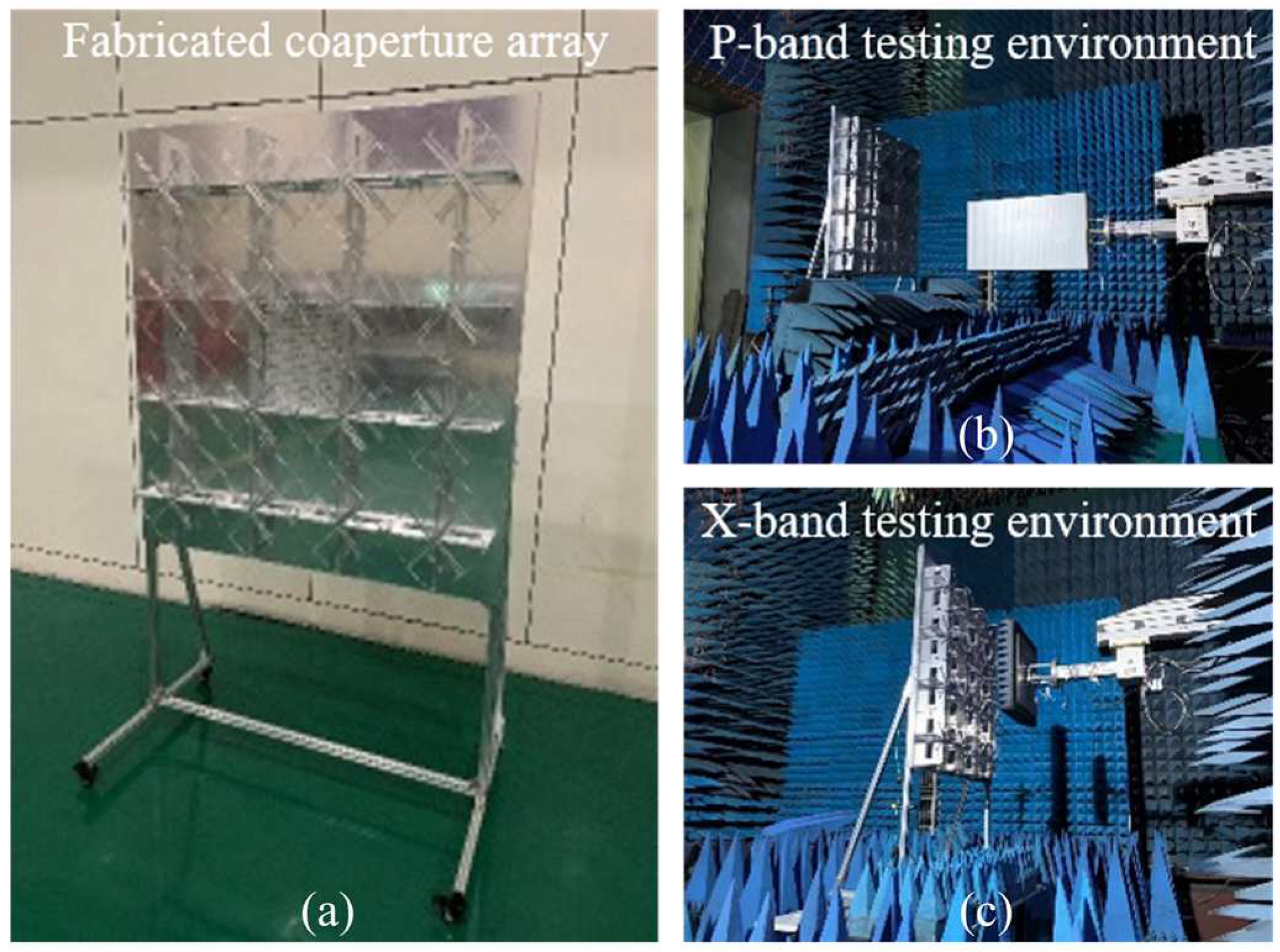
All the antenna performances were simulated with the full-wave analysis software CST STUDIO SUITE™ 2022 [30]. To verify the reliability and accuracy of the model design, a prototype was manufactured for testing after simulating various parameters. The Wiltron 37269A Network Analyzer was used to measure the reflection coefficients, and the planar near-field test system was used to measure the radiation patterns and the realized gains. The photograph of the fabricated co-aperture antenna array and the test environment is shown in Figure 7. It can be seen from the figures that due to the different tested frequency bands, the size of the probes in the test system varied significantly.
3.1. Results of P-Band Antenna Array
The following provides the simulated and measured results related to the H-polarization of the antenna array. Since the geometric structures of dual polarization are identical, presenting the test results for H-polarization is sufficient to verify the correctness of the design. The active VSWR data, the realized gains, and the E/H/D-plane patterns of the H-polarization antenna array are shown in Figure 8, Figure 9 and Figure 10. The simulation and measurement results of the active VSWRs and the realized gains are given in Figure 8. In addition to that, the plane patterns are given at 0.40 GHz, 0.55 GHz, and 0.70 GHz.
The H-polarized array has twelve RF input ports, and the active VSWRs of twelve ports are given in Figure 8. The results indicate that the active VSWRs are less than 2.0 across the entire operating range (0.4–0.7 GHz), meaning the antenna has achieved an impedance bandwidth of 54%.
In Figure 8, the simulated and measured results for the antenna array gain under normal radiation conditions (the beam of the antenna points towards the normal direction of the array) are also presented. The simulated and measured results are consistent, with the antenna array gain ranging from 14.6 to 19.5 dBi across the entire operating frequency band (0.4–0.7 GHz), and the gain increases with frequency.
The radiation patterns of the P-band antenna array are shown in Figure 9, Figure 10 and Figure 11. The simulation design results of the antenna array in normal radiation mode are found to be consistent with the measured results, with a maximum sidelobe level of 14.1 dBi within the operation band. And, in Figure 9a,b, it is proved that the half-power beam width of the H-plane and E-plane at (0.40, 0.55, and 0.70 GHz) are (31°, 23°, and 17°) and (43°, 29°, and 21°), respectively. In Figure 9c,d, the cross-polarization level (XPL) is lower than −30 dB in the H-plane and lower than −35 dB in the E-plane within the 3 dB beamwidth angle ranges at the high-frequency band. The better XPL performance can be achieved at the low-frequency band.
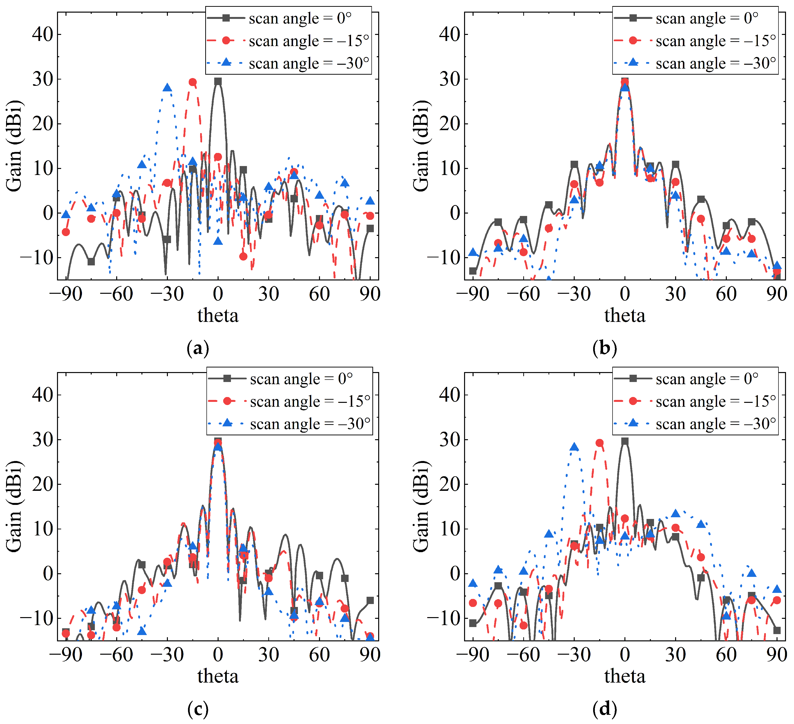
D-plane radiation performance is also good in the working frequency band, as shown in Figure 10. The XPL of the D-plane is lower than (−34.1 dB, −24.6 dB, −24.1 dB) in (400 MHz, 550 MHz, 700 MHz). The simulated results show that when the D-plane scanning angle is ±15° and ±30°, the gains are decreased by 0.4 dB and 0.9 dB and the side lobe levels are 11.5 dB and 9.4 dB, respectively at the center frequency of 0.55 GHz. The maximum values of active VSWR increase slightly with the increase in scanning angle, which are 2.2 and 2.6, respectively.
The antenna array exhibits good scanning performance within a scan range of 0 to ±30 degrees. In Figure 11, the H-plane radiation patterns for scan angles of 0°, −15°, and −30° are provided. The results show that as the scan angle increases, the gain of the antenna array decreases, and the maximum sidelobe level also increases, reaching −9.7 dB at a scan angle of 30 degrees.
3.2. Results of X-Band Antenna Subarray
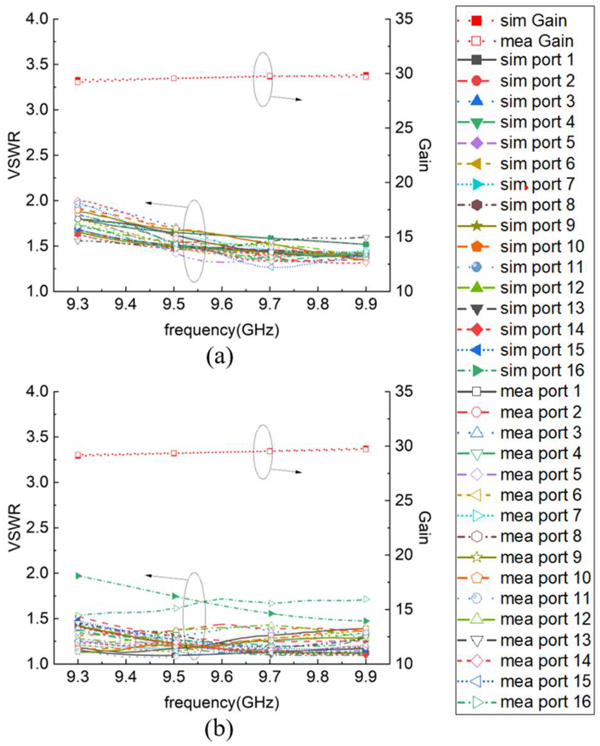
Due to the different geometrical structures of the two polarized antennas in the X-band, the results of horizontal and vertical polarized subarrays are given in Figure 12a,b, respectively. The simulation and measured impedance bandwidth of the array is 6.3% (9.3–9.9 GHz) for VSWR < 2.0. On the edge of the vertical polarization, the subarray is near to the bottom of the P-band array; in this case, the VSWRs of this edge port are different from the other ports. However, this arrangement does not affect the VSWR performance of the H-polarized subarray, and the VSWRs of each port of the H-polarized array have a good consistency. The simulation and measurement realized gains of the two polarizations are consistent, and both increase with frequency in the range of 29.1~30.2 dBi.
The simulation and measurement pattern results of the X-band subarray are also shown in Figure 13, Figure 14 and Figure 15 showing a good consistency. In the non-scanning state, the maximum sidelobe of the H-polarization subarray is less than 13.5 dBi, and that of V-polarization is less than 13.2 dBi. As expected, the XPL for H-polarization is lower than −35 dB in the H-plane and −35 dB in the E-plane within the interesting angle ranges in Figure 14a,b; the XPL for V-polarization is lower than −33 dB in the H-plane and −32 dB in the E-plane in Figure 14c,d. In the scanning state, the X-band antenna subarray can be scanned in the range of 0~±30°, and the far-field pattern shows an excellent performance. The maximum sidelobe level of H-polarization is 13.0 dBi, and 13.3 dBi for V-polarization.
Finally, a comparison of material, impendence bandwidth (IBW), and frequency tuning ratio among this study and several aforementioned designs is tabulated in Table 1. It is found that the widest frequency tuning (24.7) is obtained in this project, while an extremely wide impedance bandwidth is realized by the all-metal co-aperture array form. And, the bandwidths of the dual-band antenna array of the P-band (0.4–0.7 GHz) and X-band (9.3–9.9 GHz) are 54.5% and 6.3%, respectively.
4. Conclusions
In conclusion, an all-metal co-aperture dual-polarized antenna array is proposed in this article. And, the impedance characteristics of an ultra-wide frequency span, P-band (0.4–0.7 GHz) and X-band (9.3–9.9 GHz), are realized by using the co-aperture design, which has a bandwidth of 54.5% at the P-band and 6.3% at the X-band. The design of the hollow structures of the proposed Vivaldi not only facilitates the light-weight and low-profile design of the antennas but also has smaller interference to impedance matching of X-band antennas. Meanwhile, the design of the miniaturized slotted waveguide array also provides a metal ground for the P-band antennas. What is more, it is worth noting that the proposed antenna array also has a good performance in scanning, with a range of 0~±30°. The feasibility of the design is verified by simulating with the software CST and measuring the prototype. The simulation and measurement results show that the array has good impedance characteristics, radiation characteristics, and scanning capabilities, and is applicable to the measurement of forest biomass and other interferometric applications.
Author Contributions
Conceptualization, F.S. and X.W.; methodology, F.S.; software, Y.L.; validation, F.S., Y.L. and X.W.; formal analysis, Y.L.; writing—original draft preparation, F.S.; writing—review and editing, F.S., D.W. and X.W.; funding acquisition, D.W. All authors have read and agreed to the published version of the manuscript.
Funding
This research was funded by the National Natural Science Foundation of China, grant number 62301312.
Data Availability Statement
The data that support the findings of this study are available within the article.
Conflicts of Interest
The authors declare no conflicts of interest.
References
- Su, Y.; Lin, X.Q.; Fan, Y. Dual-band coaperture antenna based on a single-layer mode composite transmission line. IEEE Trans. Antennas Propag. 2019, 67, 4825–4829. [Google Scholar] [CrossRef]
- Huang, H.; Li, X.; Liu, Y. A novel vector synthetic dipole antenna and its common aperture array. IEEE Trans. Antennas Propag. 2018, 66, 3183–3188. [Google Scholar] [CrossRef]
- Wei, M.; Deng, H.; Sun, H.; Liu, Y. Design of an X/Ka dual-band coaperture broadband microstrip antenna array. In Proceedings of the 2011 IEEE International Conference on Microwave Technology & Computational Electromagnetics, Beijing, China, 22–25 May 2011; pp. 217–220. [Google Scholar]
- Sun, F.; Zhang, F.; Zhang, H.; Zhang, H.; Li, C.; Feng, C. A frequency diversity printed-yagi antenna element for apertures selectivity wideband array application. IEEE Trans. Antennas Propag. 2018, 66, 5634–5638. [Google Scholar] [CrossRef]
- Naik, H.; Awasthi, A.K.; Harish, A.R. Shared-aperture dual-band orthogonally polarised antenna array for L-band and S-band applications. IET Microw. Antennas Propag. 2019, 13, 431–435. [Google Scholar] [CrossRef]
- Wu, J.; Wang, C.; Guo, Y.X. Dual-band coaperture planar array antenna constituted of segmented patches. IEEE Antennas Wirel. Propag. Lett. 2020, 19, 257–261. [Google Scholar] [CrossRef]
- Liu, Y.; Yao, F.; Shang, Y. Coaperture dual-band wave-guide monopulse antenna. In Proceedings of the 2013 Proceedings of the International Symposium on Antennas & Propagation, Nanjing, China, 23–25 October 2013; pp. 685–687. [Google Scholar]
- Li, C.; Lu, X. A L/X dual-frequency coaperture microstrip array design. In Proceedings of the 2005 IEEE Antennas and Propagation Society International Symposium, Washington, DC, USA, 3–8 July 2005; Volume 1B, pp. 795–798. [Google Scholar]
- Chen, Y.; Vaughan, R.G. Dual-band shared-aperture slot array design concept. In Proceedings of the 2018 18th International Symposium on Antenna Technology and Applied Electromagnetics (ANTEM), Waterloo, ON, Canada, 19–22 August 2018; pp. 1–2. [Google Scholar]
- Feng, L.Y.; Leung, K.W. Dual-frequency folded-parallel-plate antenna with large frequency ratio. IEEE Trans. Antennas Propag. 2016, 64, 340–345. [Google Scholar] [CrossRef]
- Zhang, L.; See, K.Y.; Zhang, B.; Zhang, Y.P. Integration of dual-band monopole and microstrip grid array for single-chip tri-band application. IEEE Trans. Antennas Propag. 2013, 61, 439–443. [Google Scholar] [CrossRef]
- Zhang, J.F.; Cheng, Y.J.; Ding, Y.R.; Bai, C.X. A dual-band shared-aperture antenna with large frequency ratio, high aperture reuse efficiency, and high channel isolation. IEEE Trans. Antennas Propag. 2019, 67, 853–860. [Google Scholar] [CrossRef]
- Zhou, S.; Dong, P.; Huang, G.; Sim, C.; Li, J. Wideband antenna array with full metal structure and air-filled microstrip feeding network. IEEE Trans. Antennas Propag. 2017, 65, 3041–3048. [Google Scholar] [CrossRef]
- Yilmaz, B.A.; Dogan, D. A dual polarized all metal wideband vivaldi array with wide scan ability. In Proceedings of the 2017 IEEE International Symposium on Antennas and Propagation & USNC/URSI National Radio Science Meeting, San Diego, CA, USA, 9–14 July 2017; pp. 309–310. [Google Scholar]
- Ma, L.; Guan, L.; Li, T.; Fan, Z.; Chen, R. Ultra-wideband all-metal vivaldi phased array antenna with metal baffles. In Proceedings of the 2018 International Applied Computational Electromagnetics Society Symposium-China (ACES), Beijing, China, 29 July–1 August 2018; pp. 1–2. [Google Scholar]
- Kindt, R.W.; Pickles, W.R. Ultrawideband all-metal flared-notch array radiator. IEEE Trans. Antennas Propag. 2010, 58, 3568–3575. [Google Scholar] [CrossRef]
- Huang, G.; Zhou, S.; Chio, T.; Yeo, T. Fabrication of a high-efficiency wave-guide antenna array via direct metal laser sintering. IEEE Antennas Wirel. Propag. Lett. 2016, 15, 622–625. [Google Scholar] [CrossRef]
- Zhou, S.; Huang, G.; Chio, T. A lightweight, wideband, dual-circular-polarized wave-guide cavity array designed with direct metal laser sintering considerations. IEEE Trans. Antennas Propag. 2018, 66, 675–682. [Google Scholar] [CrossRef]
- Kindt, R.; Mital, R.; Logan, J.; Lee, M.; Vouvakis, M. A 6:1 bandwidth PUMA array at 7 mm scale. In Proceedings of the 2016 IEEE International Symposium on Phased Array Systems and Technology (PAST), Waltham, MA, USA, 18–21 October 2016; pp. 1–4. [Google Scholar]
- Chen, Z.; Zhou, S.; Chio, T. A class of all metal cavity-backed slot array with direct metal laser sintering. IEEE Access 2018, 6, 69650–69659. [Google Scholar] [CrossRef]
- Guennou-Martin, A.; Quéré, Y.; Rius, E.; Fourtinon, L.; Person, C.; Lesueur, G.; Merlet, T. Design and manufacturing of a 3-D conformal slotted wave-guide antenna array in Ku-band based on Direct Metal Laser Sintering. In Proceedings of the 2016 IEEE Conference on Antenna Measurements & Applications (CAMA), Syracuse, NY, USA, 23–27 October 2016; pp. 1–4. [Google Scholar]
- Wu, X.; Yang, F.; Xu, F.; Zhou, J. Circularly polarized wave-guide antenna with dual pairs of radiation slots at Ka-band. IEEE Antennas Wirel. Propag. Lett. 2017, 16, 2947–2950. [Google Scholar] [CrossRef]
- Hirokawa, J.; Ito, S.; Suetsugu, S.; Zhang, M.; Ando, M. Fabrication of a double-layer corporate-feed wave-guide slot array by powder metal laser process. In Proceedings of the 2014 International Conference on Numerical Electromagnetic Modeling and Optimization for RF, Microwave, and Terahertz Applications (NEMO), Pavia, Italy, 14–16 May 2014; pp. 1–4. [Google Scholar]
- Shi, B.; Ke, T.; Luo, Q. Scanned slot array fed by inclined slots in ridge wave-guide. In Proceedings of the 2017 Sixth Asia-Pacific Conference on Antennas and Propagation (APCAP), Xi’an, China, 16–19 October 2017; pp. 1–3. [Google Scholar]
- Zhou, J.; Wang, H.; Cao, J.; Liang, G.; Jiang, S. Ridged wave-guide slot phased array for 5G millimeter-wave application. In Proceedings of the 2019 Cross Strait Quad-Regional Radio Science and Wireless Technology Conference (CSQRWC), Taiyuan, China, 18–21 July 2019; pp. 1–3. [Google Scholar]
- Zheng, Z.; Fang, X.; Wang, W.; Huang, G.; Zhang, H.; Liang, X. A compact wave-guide slot filtering antenna based on mushroom-type surface. IEEE Antennas Wirel. Propag. Lett. 2020, 19, 1823–1827. [Google Scholar] [CrossRef]
- Magnusson, P.; Di Salvo, M.; Scarchilli, C. A dual polarised slotted wave-guide antenna for satellite based wind scatterometer instruments. In Proceedings of the 2013 7th European Conference on Antennas and Propagation (EuCAP), Gothenburg, Sweden, 8–12 April 2013; pp. 3565–3568. [Google Scholar]
- Mallahzadeh, A.R.; Nezhad, S.M.A. Cross-polarization and size reduction of slotted wave-guide array antenna by angled ridges. In Proceedings of the 2012 6th European Conference on Antennas and Propagation (EUCAP), Prague, Czech Republic, 26–30 March 2012; pp. 1–5. [Google Scholar]
- Tian, J.; Sun, G. Design of K-band single ridge wave-guide slot antenna arrays. In Proceedings of the 2017 2nd IEEE International Conference on Integrated Circuits and Microsystems (ICICM), Nanjing, China, 8–11 November 2017; pp. 291–294. [Google Scholar]
- CST Studio SuiteTM. Available online: https://www.cst.com (accessed on 10 March 2024).
Figure 1.
The schematic of the co-aperture array.

Figure 2.
The optimization processes of P-band antenna (units: mm). (a) A typical metal Vivaldi. (b) Low-profile processed. (c) Hollowed.
Figure 2.
The optimization processes of P-band antenna (units: mm). (a) A typical metal Vivaldi. (b) Low-profile processed. (c) Hollowed.
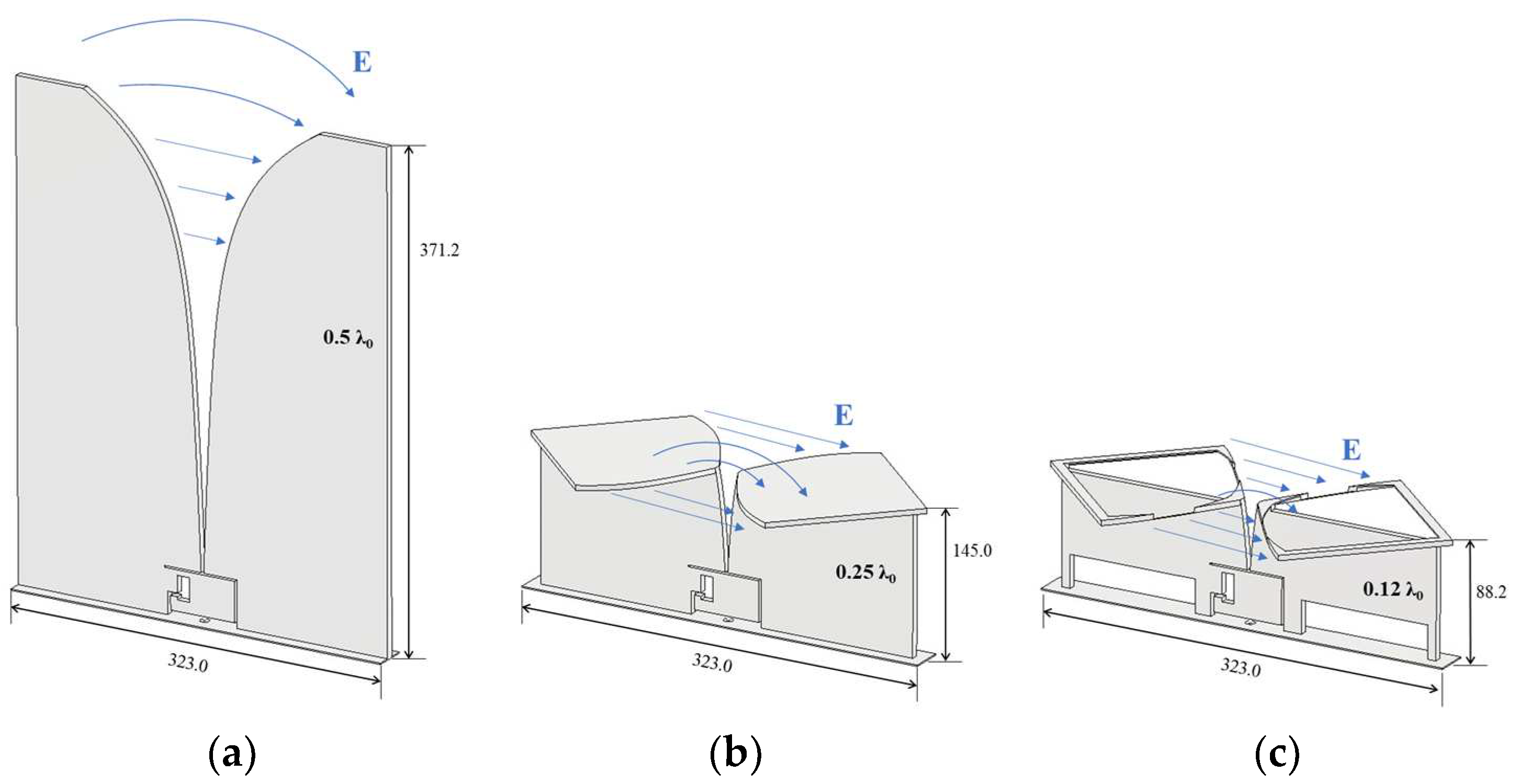
Figure 3.
Designs for P-band antenna array without the metal ground (units: mm).
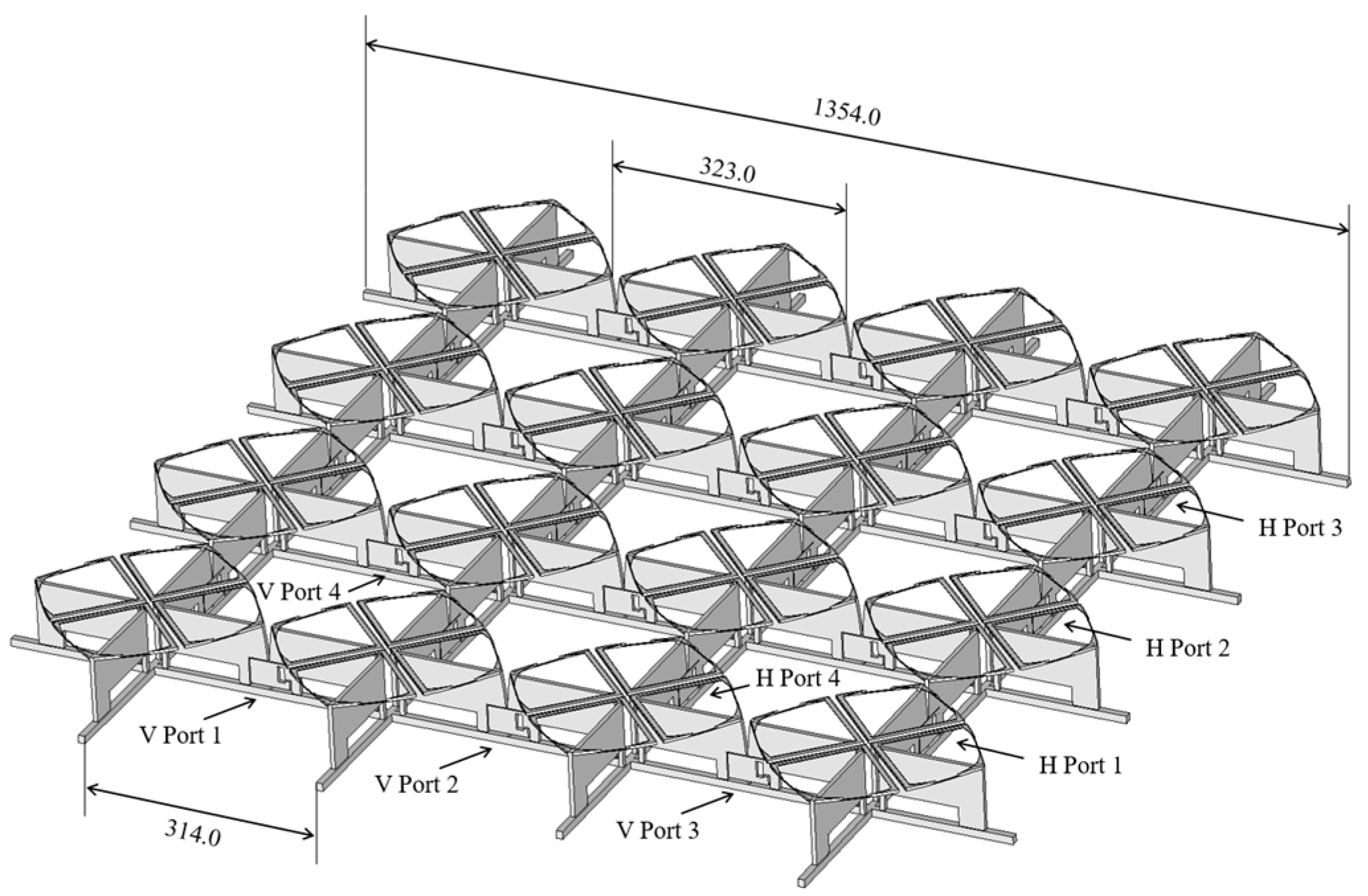
Figure 4.
Structure dimensions for P-band antenna element (units: mm).
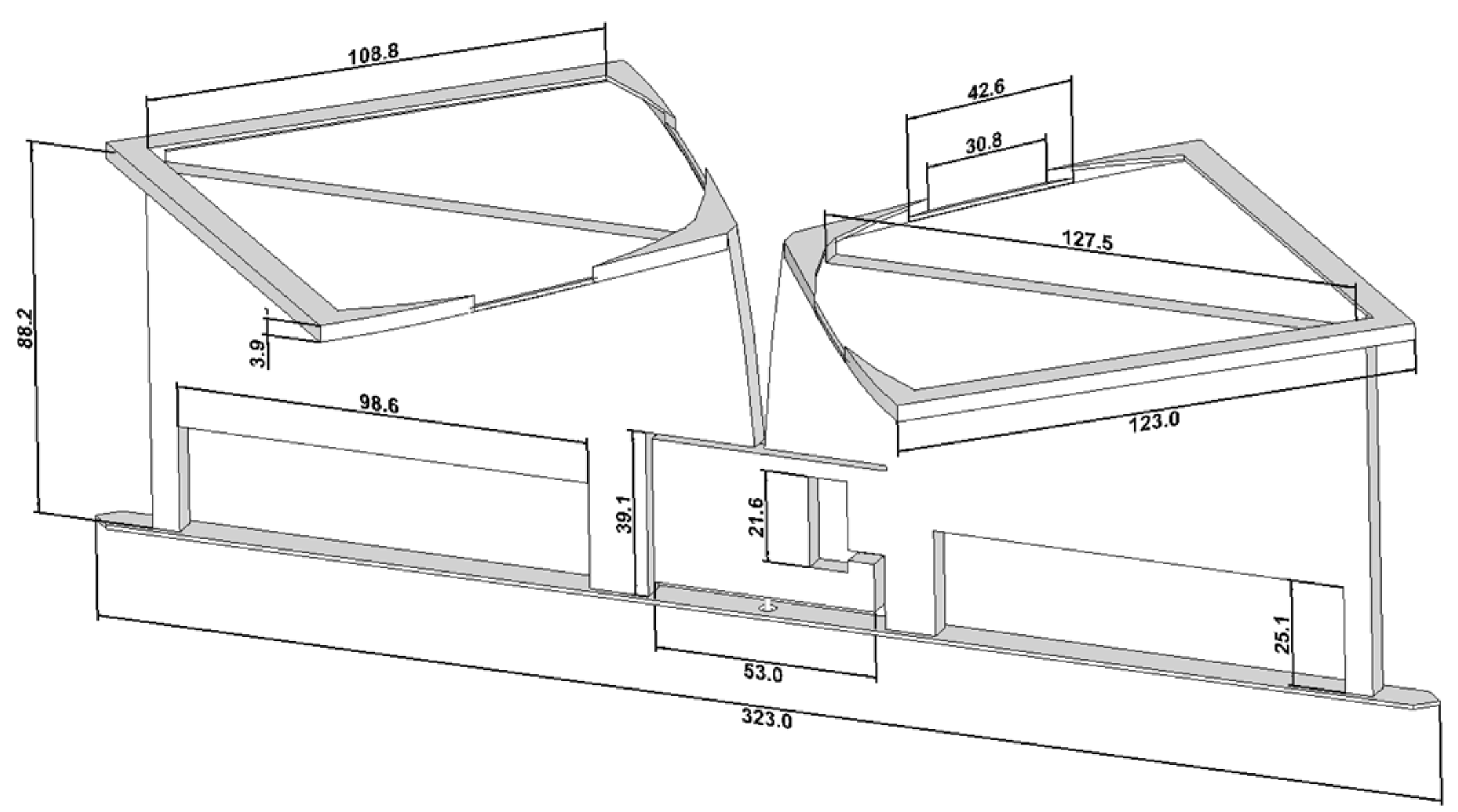
Figure 5.
Designs and structure dimensions for X-band antenna (units: mm).
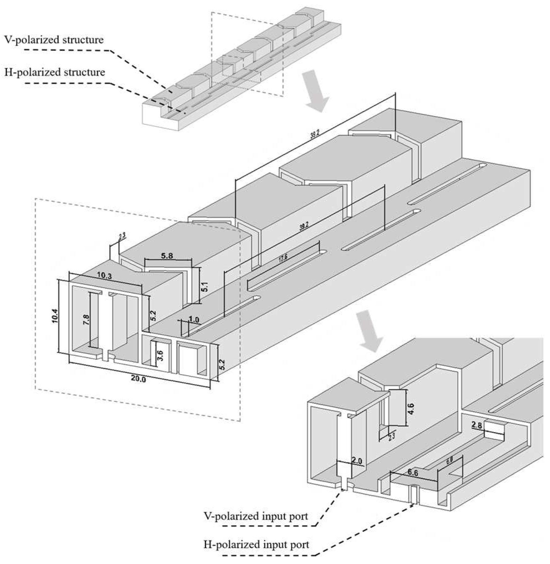
Figure 6.
Designs for X-band antenna subarray (units: mm).
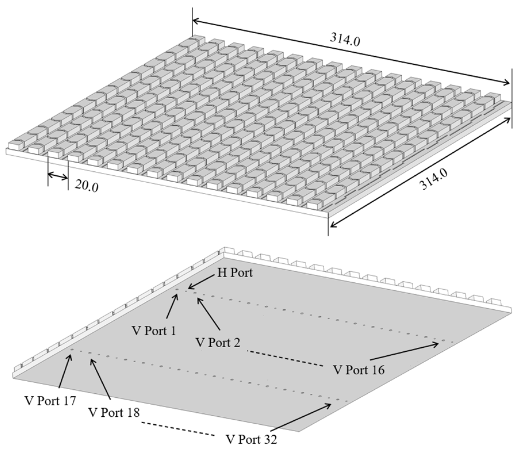
Figure 7.
(a) Fabricated co-aperture antenna array with side views. (b) P-band testing environment. (c) X-band testing environment.
Figure 7.
(a) Fabricated co-aperture antenna array with side views. (b) P-band testing environment. (c) X-band testing environment.

Figure 8.
Simulated and measured VSWRs and gains.
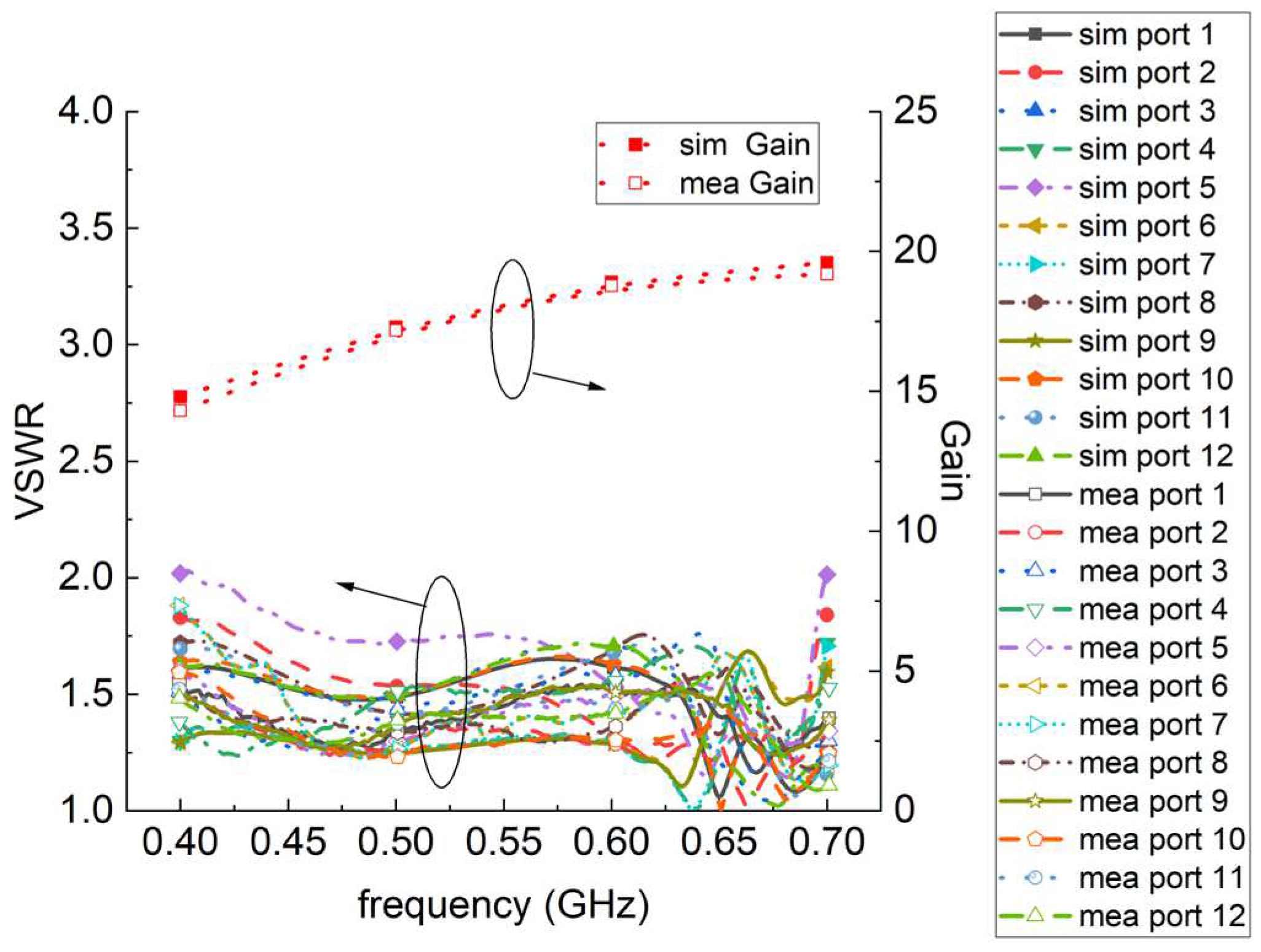
Figure 9.
Simulated and measured comparison pattern results of (a) H-plane and (b) E-plane; cross-polarization results of (c) H-plane and (d) E-plane.
Figure 9.
Simulated and measured comparison pattern results of (a) H-plane and (b) E-plane; cross-polarization results of (c) H-plane and (d) E-plane.
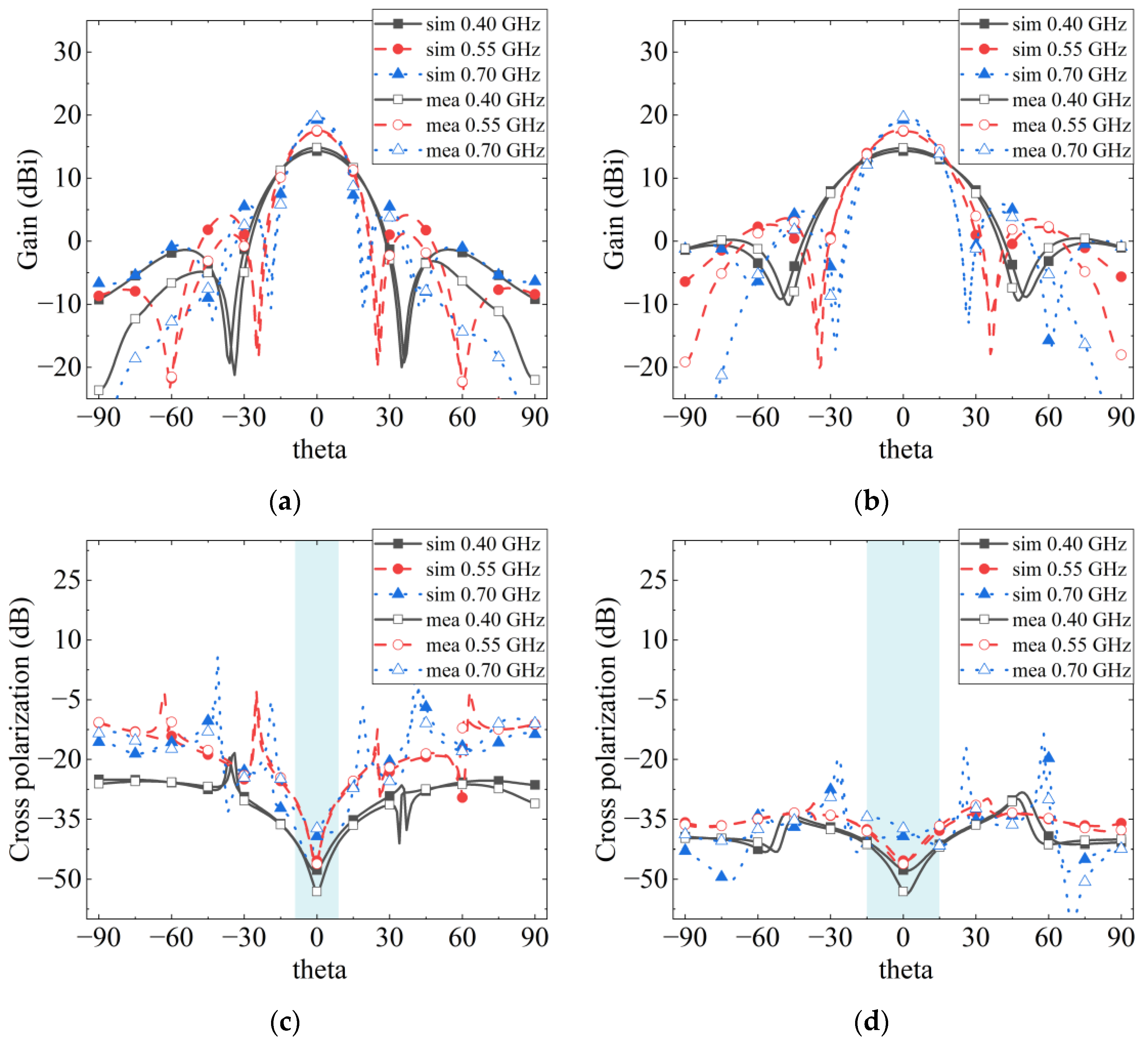
Figure 10.
Simulated radiation performance on D-plane of (a) pattern; (b) cross polarization at 0.40 GHz, 0.55 GHz, and 0.70 GHz.
Figure 10.
Simulated radiation performance on D-plane of (a) pattern; (b) cross polarization at 0.40 GHz, 0.55 GHz, and 0.70 GHz.
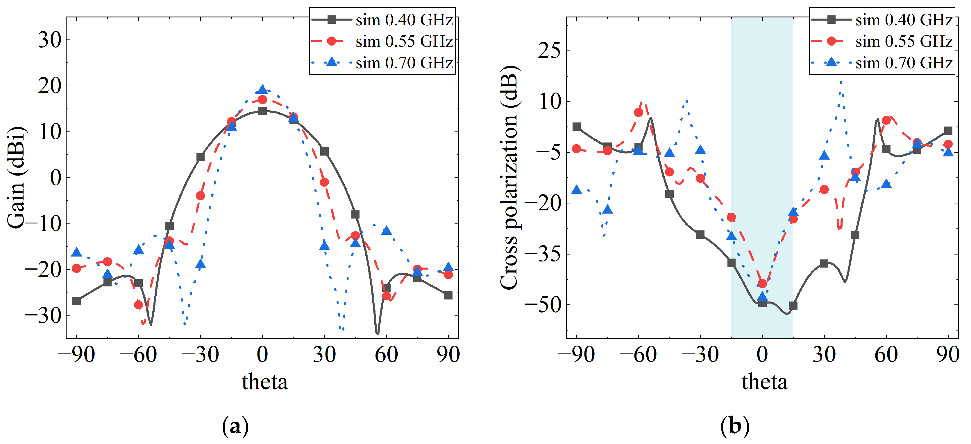
Figure 11.
Simulated pattern results of (a) H-plane and (b) E-plane of 0°, −15°, −30° scanning angle at 0.55 GHz.
Figure 11.
Simulated pattern results of (a) H-plane and (b) E-plane of 0°, −15°, −30° scanning angle at 0.55 GHz.
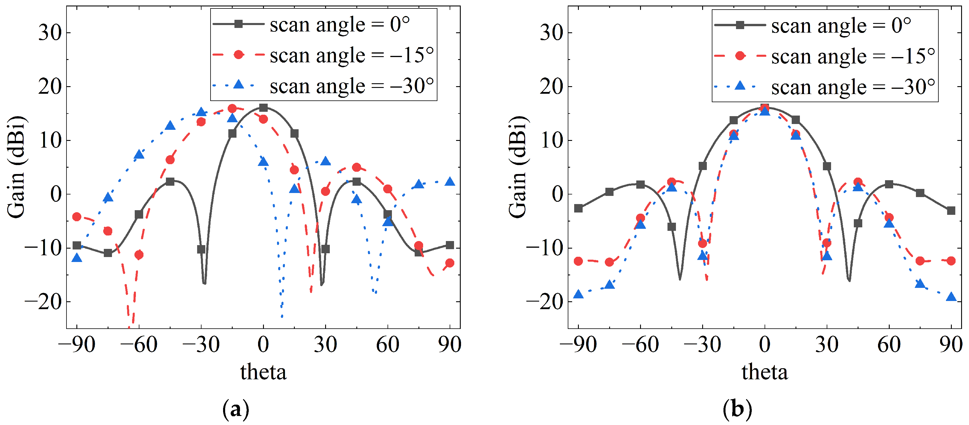
Figure 12.
Simulated and measured active VSWRs and realized gains of (a) H-polarization and (b) V-polarization.
Figure 12.
Simulated and measured active VSWRs and realized gains of (a) H-polarization and (b) V-polarization.

Figure 13.
Simulated and measured pattern results of (a) H-plane and (b) E-plane for H-polarization, and (c) H-plane and (d) E-plane for V-polarization at 9.3 GHz, 9.6 GHz, and 9.9 GHz.
Figure 13.
Simulated and measured pattern results of (a) H-plane and (b) E-plane for H-polarization, and (c) H-plane and (d) E-plane for V-polarization at 9.3 GHz, 9.6 GHz, and 9.9 GHz.
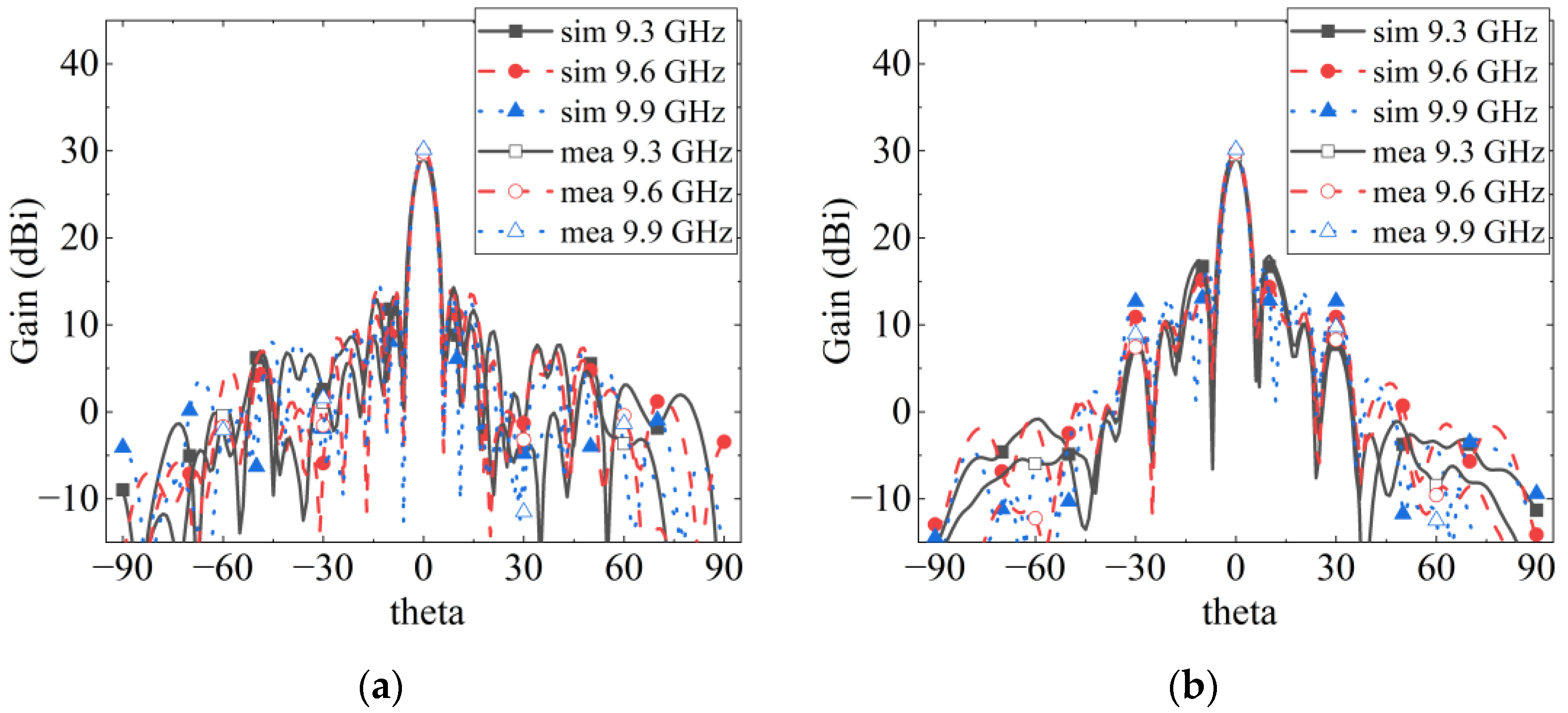
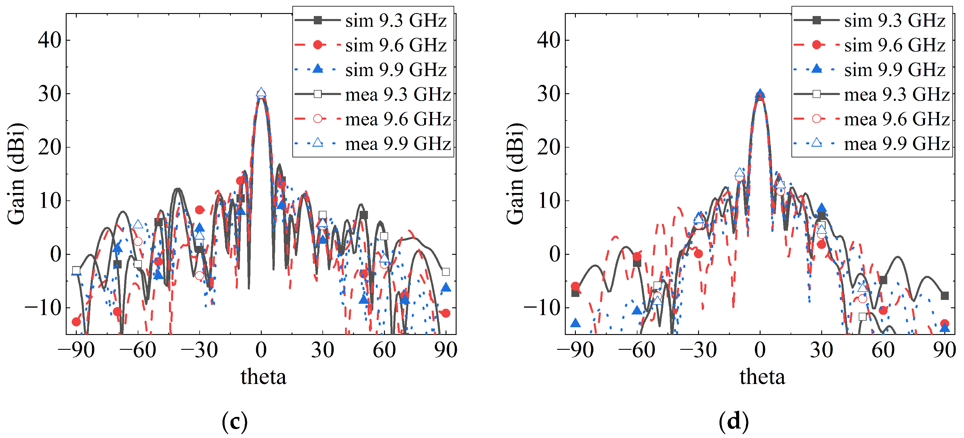
Figure 14.
Simulated and measured cross-polarization characteristic of (a) H-plane and (b) E-plane for H-polarization, and (c) H-plane and (d) E-plane for V-polarization at 9.3 GHz, 9.6 GHz, and 9.9 GHz.
Figure 14.
Simulated and measured cross-polarization characteristic of (a) H-plane and (b) E-plane for H-polarization, and (c) H-plane and (d) E-plane for V-polarization at 9.3 GHz, 9.6 GHz, and 9.9 GHz.
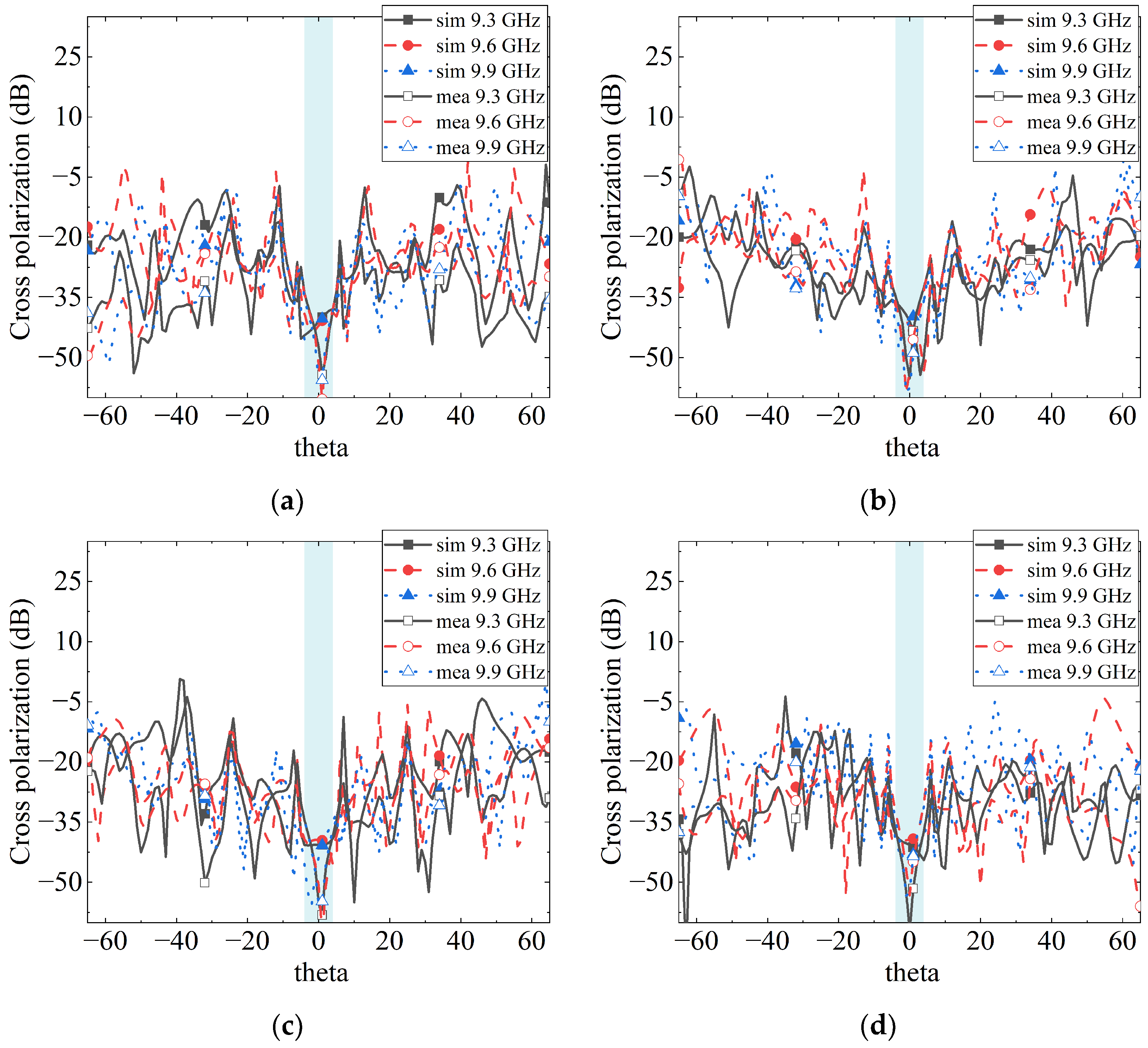
Figure 15.
Simulated pattern results of (a) H-plane and (b) E-plane for H-polarization, and (c) H-plane and (d) E-plane for V-polarization of 0°, −15°, and −30° scanning angle at 9.6 GHz.
Figure 15.
Simulated pattern results of (a) H-plane and (b) E-plane for H-polarization, and (c) H-plane and (d) E-plane for V-polarization of 0°, −15°, and −30° scanning angle at 9.6 GHz.

Table 1.
Comparison of the co-aperture array in this letter with other arrays.
| Ref. | Material | Freq. (GHz) | IBW (%) | Array | Freq. Tuning Ratio |
|---|---|---|---|---|---|
| [2] | Dielectric | 8.6~9.9 | 14.1 | Yes | 4.2 |
| 32.0~36.0 | 11.8 | Yes | |||
| [3] | Dielectric | 1.3~1.36 | 4.5 | Yes | 2.5 |
| 2.6~3.3 | 23.7 | Yes | |||
| [5] | Dielectric | 0.8~1.3 | 54 | Yes | 4.6 |
| 3.0~3.7 | 25 | Yes | |||
| [10] | Metal | 2.17~2.63 | 9.7 | No | 11.3 |
| 23.5~24.5 | 2.1 | Yes | |||
| [11] | Dielectric | 4.76~5.56 | 15.2 | No | 13.4 |
| 57.0~64.0 | 11.4 | Yes | |||
| [12] | Dielectric | 3.4~3.51 | 2.9 | No | 17.6 |
| 58.6~60.0 | 2.4 | Yes | |||
| Our work | Metal | 0.4~0.7 | 54.5 | Yes | 24.7 |
| 9.3~9.9 | 6.3 | Yes |
Disclaimer/Publisher’s Note: The statements, opinions and data contained in all publications are solely those of the individual author(s) and contributor(s) and not of MDPI and/or the editor(s). MDPI and/or the editor(s) disclaim responsibility for any injury to people or property resulting from any ideas, methods, instructions or products referred to in the content. |
© 2024 by the authors. Licensee MDPI, Basel, Switzerland. This article is an open access article distributed under the terms and conditions of the Creative Commons Attribution (CC BY) license (https://creativecommons.org/licenses/by/4.0/).
Share and Cite
MDPI and ACS Style
Sun, F.; Wu, X.; Luan, Y.; Wang, D. A P/X Dual-Band Co-Aperture Array with Dual-Polarized Antenna Based on Forest Biomass Measurement Applications. Electronics 2024, 13, 1565. https://doi.org/10.3390/electronics13081565
AMA Style
Sun F, Wu X, Luan Y, Wang D. A P/X Dual-Band Co-Aperture Array with Dual-Polarized Antenna Based on Forest Biomass Measurement Applications. Electronics. 2024; 13(8):1565. https://doi.org/10.3390/electronics13081565
Chicago/Turabian StyleSun, Fukun, Xian Wu, Yuchen Luan, and Duo Wang. 2024. "A P/X Dual-Band Co-Aperture Array with Dual-Polarized Antenna Based on Forest Biomass Measurement Applications" Electronics 13, no. 8: 1565. https://doi.org/10.3390/electronics13081565
Note that from the first issue of 2016, this journal uses article numbers instead of page numbers. See further details here.