
High-Speed CNN Accelerator SoC Design Based on a Flexible Diagonal Cyclic Array
by
 , and
, and
Dong-Yeong Lee
1,
Hayotjon Aliev
1,
Muhammad Junaid
1,
Sang-Bo Park
1,
Hyung-Won Kim
1,
Keon-Myung Lee
2 and
Sang-Hoon Sim
1,* 1
Department of Electronics Engineering, Chungbuk National University, Cheongju 28644, Republic of Korea
2
Department of Computer Science, Chungbuk National University, Cheongju 28644, Republic of Korea
*
Author to whom correspondence should be addressed.
Electronics 2024, 13(8), 1564; https://doi.org/10.3390/electronics13081564
Submission received: 20 March 2024
/
Revised: 17 April 2024
/
Accepted: 17 April 2024
/
Published: 19 April 2024
(This article belongs to the Special Issue CMOS Integrated Circuits Design)
Abstract
:The latest convolutional neural network (CNN) models for object detection include complex layered connections to process inference data. Each layer utilizes different types of kernel modes, so the hardware needs to support all kernel modes at an optimized speed. In this paper, we propose a high-speed and optimized CNN accelerator with flexible diagonal cyclic arrays (FDCA) that supports the acceleration of CNN networks with various kernel sizes and significantly reduces the time required for inference processing. The accelerator uses four FDCAs to simultaneously calculate 16 input channels and 8 output channels. Each FDCA features a 4 × 8 systolic array that contains a 3 × 3 processing element (PE) array and is designed to handle the most commonly used kernel sizes. To evaluate the proposed CNN accelerator, we mapped the widely used YOLOv5 CNN model and evaluated the performance of its implementation on the Zynq UltraScale+ MPSoC ZCU102 FPGA. The design consumes 249,357 logic cells, 2304 DSP blocks, and only 567 KB BRAM. In our evaluation, the YOLOv5n model achieves an accuracy of 43.1% ([email protected]). A prototype accelerator has been implemented using Samsung’s 14 nm CMOS technology. It achieves 1.075 TOPS, a peak performance with a 400 MHz clock frequency.
1. Introduction
Convolutional neural networks are widely used in a wide range of applications for image recognition and object detection. Compared to other computer vision algorithms, CNNs offer a significant improvement in accuracy for object recognition, target detection, and video tracking. As a result, CNN models have become popular and have played a crucial role in the rapid advancement of computer vision applications. Meanwhile, CNN models are becoming more complex, using different kernel sizes and applying more depth and scale of CNN networks to achieve higher prediction accuracy. These advancements and changes in CNN models have a significant impact on the performance of the storage and processing capabilities of current hardware accelerators. Thus, new acceleration architectures for object detection CNN models are necessary, applying efficient data streaming, storing, and processing methods [1].
Most CNN models comprise a series of multiple convolutional layers, and each layer is convolved with different sized kernels. For example, our target CNN model is the YOLOv5 object detector, which is made up of 99% convolutional computations with various kernel sizes [2]. Accelerating YOLO-like CNN networks on hardware devices can significantly improve their inference speed, enabling faster execution compared to traditional CPU or GPU implementations. Furthermore, it is essential to optimize the computations in the convolution operation to support various kernel sizes when designing a new high-speed CNN accelerator. These kernel-based optimizations of convolution operation blocks help to map any CNN models to the hardware accelerator.
Most of the CNN accelerator architectures use parallel processing element (PE) units, which consist of a multiplier and accumulator (MAC), as shown in Figure 1. A systolic array is a special PE array structure built for the fast and efficient operation of regular array algorithms and to reduce their computation time. The systolic arrays are also effective at reducing memory access by reusing data that have already been passed through other PEs. Therefore, many research works have proposed systolic array architectures to maximize the speed of iterative convolution computations [3,4,5,6,7,8,9,10,11,12,13,14].
In many CNN models, the convolutional layer uses a stride of 2 to convolve the input data with a 3 × 3 kernel, which is faster than using a stride of 1. A convolutional layer with a stride of 2 is advantageous in that it requires less computation. The filter moves two pixels at a time over the input feature map, which results in faster down-sampling of the input. However, most research on CNN accelerators shows that the time consumption for stride 2 is the same as for the stride 1 mode. The reason for this is that the feature map data are supplied to the PE in the same way as the 3 × 3 stride 1 kernel mode, and it produces relatively low PE utilization. This indicates that the stride 2 mode is not as efficiently implemented as the stride 1 mode on CNN accelerators [15].
In this paper, we propose a hardware architecture for a CNN inference accelerator, using a novel systolic array architecture called the flexible diagonal cyclic array (FDCA) to accelerate the convolution operation and support various kernel sizes, including the 3 × 3 kernel with stride 2. This paper introduces the following new methods to minimize repeated memory accesses, optimize hardware resources for various kernel modes, and enable the mapping of diverse CNN models onto a wide range of FPGA devices.
- Flexible Diagonal Cyclic Array (FDCA) for kernel modes: The FDCA is a novel systolic array structure designed to maximize data reuse and speed up computation by efficiently performing convolutions. In the FDCA, PEs are arranged in a 3 × 3 systolic array. Multiplication and accumulation operations are performed to calculate a partial sum, which is then forwarded to the diagonal PEs to accumulate the output result. In this study, we optimized a DCA systolic array for the convolution operation using a 3 × 3 kernel with strides of 1 and 2, which are commonly used in CNN accelerators.
- Input Zero Padding: The CNN accelerator supports adding zero-padding data to the around the input feature map. When the CNN accelerator reads the input feature map from DDR, it decides to add input zero padding at the corresponding position. This function provides several advantages, such as reducing DDR access and effectively utilizing on-chip memory, instead of writing padding data for the output feature map. To implement input padding, we designed the input zero padding circuit, which utilizes a 2-bit register to indicate the status required for each situation and a wire to control the global input buffer read enable signal.
- Reconfigurable Input FIFO and FIFO Output Cache Memory: The reconfigurable input FIFO consists of three SRAM FIFOs and one register connected in a predefined sequence. When we define the kernel mode for a convolutional operation using a specific stride and kernel size, the reconfigurable input FIFOs are interconnected according to the kernel mode to efficiently reuse the data. The data that are read from the first FIFO will flow to another FIFO and systolic array processing, respectively.The FIFO output cache memory is a register that supplies a large amount of data to the PE. It can transfer two different data to the PE depending on the kernel mode. By using the address for this register, it enables the activation of the “read enable” for the reconfigurable input FIFO connected to the register and generating a “write enable” signal for the register, allowing data to be read sequentially whenever needed.
- Weight Parameter Quantization: Quantization is a method for reducing model size by converting model weights, biases, and activations from high-precision floating-point representation to low-precision floating-point (FP) or integer (INT) representations, such as 16-bit or 8-bit. By converting the weights of a model from high-precision floating-point representation to lower precision, the model size and inference speed can significantly improve without sacrificing too much accuracy. Additionally, quantization improves the model performance by reducing memory bandwidth requirements and increasing resource utilization [16].
In this work, we used 32-bit floating point parameters for training and then quantized them to 8-bit integers to enable high-speed lightweight CNN inference. By applying a low-bit quantization, we can utilize small-size on-chip memory, multipliers, and adders.
The rest of this paper is organized as follows: In Section 2, the background of the overall architecture of the CNN Accelerator is described. A detailed explanation of the proposed flexible PE array architecture is given in Section 3. In Section 4, we outlined the advantages of using the proposed architecture. Section 5 includes the verification process and the results obtained. Section 6 concludes the paper with future research plans.
2. Related Work and Motivation
Many researchers have studied lightweight object detectors and proposed hardware accelerators to accomplish real-time object detection on edge devices. The acceleration of CNN model inference for object detection is discussed in more detail, with a focus on FPGA-based implementations. Thus, various hardware architecture approaches and optimization methods are explored to examine their impact on throughput and accuracy [17,18,19,20,21,22,23,24,25,26].
Since its initial release [27] in 2016, several versions of YOLO have been developed and accelerated for improving the processing efficiency. The problem is that designing a new dedicated accelerator for a new version of YOLO is a time-consuming process.
Most of the studies analyze the acceleration of the YOLOv2 algorithm to improve development speed, power efficiency, and computing performance. Many analyses provide developers with new insights for choosing hardware and architectures to optimize the YOLOv2 algorithm [14,28,29].
The lightweight YOLO versions, including Tinier-YOLO, Tiny-YOLOv3, and Tiny-YOLOv4, have fewer parameters and require fewer computations compared to the full versions. However, they also exhibit some reduction in accuracy. They are deployed on FPGA-based embedded computing platforms and have achieved better real-time detection results, utilizing architectures with high performance and low energy consumption [30,31,32]. The accelerators have been configured to run Tiny-YOLOv3 [30] and Tiny-YOLOv4 [32] in real time, achieving performance of over 8.3 and 30 frames per second.
Other studies [13,25,26,33,34] have investigated the implementation of the entire CNN-based object detection networks on FPGA devices by building customized computation units and data flows into their accelerator designs. As a result, the impact of data communication bottlenecks is minimized and the overall performance is enhanced. However, the accelerator designs proposed in these works are tailored to specific versions of the YOLO network and lack the versatility to target more recent object detection models.
This paper introduces a novel architecture that enables the deployment of the next generation of models from the YOLO family on a variety of FPGA devices. Our proposed toolflow is designed to efficiently process YOLOv5 and the latest YOLO models, offering high performance and reconfigurability to accommodate new changes and architecture updates. To achieve efficient implementation of YOLOv5-based algorithms, we conducted research on various customized hardware accelerators and proposed new methods to optimize them.
3. Overall Hardware Architecture
Figure 2 illustrates the overall architecture of the proposed CNN accelerator. The architecture consists of the following hardware block components: PE arrays block with four FDCAs, 5 × 5 max-pooling, element-wise adder, upsampling, global in/output buffer, AXI4 data bus, and CNN controller blocks.
In this study, we introduce a new systolic array (SA) structure called the flexible diagonal cyclic array (FDCA) that also supports the stride 2 kernel mode. The SA structure is designed in the form of an array of 3 × 3 PEs, called a kernel unit (KU), to optimize the convolution operation using a 3 × 3 kernel with stride 1. In general, each PE computes a partial sum of the convolution and sends it to other PEs to generate a single convolution result using an accumulator. If the CNN model includes a layer with N × N filters, the proposed PE array can be easily configured to support the required kernel size and stride. The FDCA consists of 4 × 8 KUs, with each KU with 9 PEs, and it can simultaneously process four input channels and eight output channels.
3.1. Four FDCA for Convolution Acceleration
To accelerate the convolution operation, we employ four FDCAs to calculate 16 input data channels simultaneously. The relevant processing architecture is illustrated in Figure 3. The convolutional result generated by a single filter using FDCA is stored in a convolutional memory (Conv_mem). After calculating the convolutional outputs for all input channels, the final result is produced by accumulating them and storing the result in the Conv_mem as the final output.
In addition, the four-FDCA architecture is specially designed to maximize data reuse and speed up the processing of the convolutional layer. Therefore, optimized data reuse on KUs of the architecture provides a higher utilization ratio in any 3 × 3 or 6 × 6 kernel modes compared to previous studies.
3.2. Max Pooling
The max pooling operation compares 25 input feature maps and produces the largest value from them. For the max pooling operation, we designed a 5 × 5 max pooling hardware block that is composed of 128 comparators. The max pooling block includes 16 in/out flip-flop memories and a (de)channeling controller that is used to reorder and write data back to DDR.
3.3. Element-Wise Adder
The element-wise adder is a hardware architecture designed to perform element-wise addition of data from two different feature maps with equal size. The hardware block consists of parallel adders and input/output buffers. The concept of element-wise addition operation is derived from the latest YOLO models, which merge data from two streams.
3.4. Upsampling (Resize)
Upsampling is a novel hardware sub-circuit used to increase the size of the input feature map. For an input feature map with a size of n × n, the upsampling layer increases the output feature map size to 2n × 2n by making an exact copy of each input feature map and placing it at the bottom, right, and bottom-right diagonal pixel positions.
3.5. Global Input/Output Buffers and AXI4 Data Bus
In the proposed architecture, the global input/output buffers are used for sending/receiving data to/from DDR via the 256-bit AXI4 data bus. The proposed architecture includes an additional input buffer called “Instruction Memory”, which is used for writing the instruction microcode from the RISC-V CPU core through the 32-bit AXI4-Lite bus protocol.
3.6. CNN Controller
The CNN controller hardware block controls the processing of functional hardware blocks in the proposed design, such as the four FDCAs for convolution acceleration, 5 × 5 max pooling, element-wise adder, and upsampling. The CNN controller uses microcode information to manage all data processing operations, from reading input data to the processing hardware block from a predefined address to writing output data to DDR DRAM using AXI4 transactions.
4. The Proposed CNN Accelerator
4.1. Stride in Convolutional Operation
The stride defines the number of moving steps of the filter through the input feature map to generate an output value. If the stride is bigger than one (>1), the output feature map size decreases compared to the input.
Equation (1) defines the output feature map size (o) for a given stride (s), where i is the input feature map size, k is the kernel size, and p is the padding added to the input feature map.
Most CNN accelerators only use a stride of 1 when shifting a kernel over an input. In this article, we introduce a new method for implementing stride 2 convolution on hardware.
4.2. Convolution Using Kernel 3 × 3 with Stride 1 in Kernel Unit
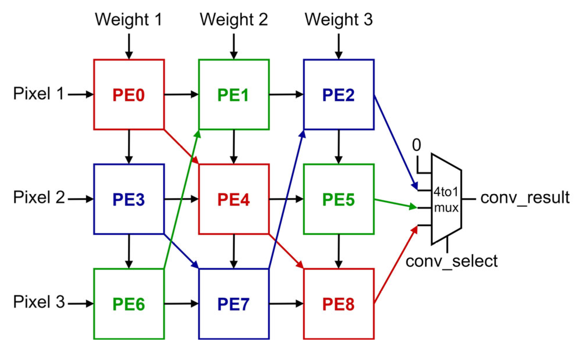
The convolution operation using a 3 × 3 kernel with a stride of 1 is a basic kernel mode that utilizes the entire 3 × 3 PE array structure, known as the KU. In this work, the filter convolves the input feature map in a direction from up to down; the kernel is shifted vertically over the input feature map with a stride of 1. In the KU, pixel data moves horizontally from left to right and is reused for one clock cycle in each PE. The weights move vertically, from up to down. The weights will be reused in every clock cycle in the KU. In each clock cycle, FIFOs supply three pixels and weight data values to the KU. Each PE transfers its accumulated value to the bottom-right diagonal PE over KU, during the processing. As shown in Figure 4, PE6 and PE7 do not have bottom-right diagonal PEs. Therefore, these PEs transfer accumulated values to PE1 and PE2, respectively.
The PE2, PE5, and PE8 perform convolution operations for one input channel by accumulating nine data, including six data accumulated by the Pes of the previous two vertical lines. The last vertical line produces one convolution result in every clock cycle after the first result is produced. Since only one final result is produced in KU for each clock, the conv_select signal is reused to select the results sequentially. The color of each PE and arrow indicates the path of partial sums used to compute one convolution result. The convolution results are repeatedly calculated in the order of red, blue, and green.
4.3. Convolution Using Kernel 3 × 3 with Stride 2 in Kernel Unit
The convolution operation with a 3 × 3 kernel and a stride of 2 uses the same PE array architecture, known as the KU, as that used for a stride of 1. However, in the stride 2 mode, data sharing between PEs differs; the data accumulated in each PE will be transferred horizontally to the next PE, not diagonally. To perform a convolution operation with a stride of n (n > 1), six pixels of data must be loaded into the KU at the same time. We used a FIFO output cache memory between the reconfigurable input FIFO and KU to prepare data for further processing in PEs. Using this cache memory, we can read two pixels of data from the input FIFO at the same time.
As illustrated in Figure 5, the first three pixels of data will be sent to the PEs in the first column, as seen in the stride 1 mode. The next three pixels of data from the cache register will be simultaneously sent to the second-column PEs. After completing clock calculations in PEs, we have to pass the pixel values from the first-column PEs to the last-column PEs. In this order, we maintain the convolution operation with stride 2, efficiently reusing the data from the first-column PEs. Pixel data values from the first column PEs of the KU will be transferred to the diagonally downward PEs in the last column. This means that data reuse only occurs in the first and third columns of the KU, specifically in the stride 2 mode. In addition, weights are reused in every clock cycle by vertically rotating them from top to bottom.
Figure 6b illustrates an example of a convolution operation with stride 2, representing motion of the filter over the input feature data.
4.4. Convolution Using Kernel 1 × 1 with Stride 1 in Kernel Unit
Using the proposed 3 × 3 PEs array of KU, we can run the convolution operation using a 1 × 1 kernel size with a stride of 1. For the 1 × 1 convolution operation, we have designed an accelerator circuit that exclusively utilizes the first horizontal line of PEs in the KU unit. In this mode, the upper left PE receives only one datum in every clock cycle, while the upper right PE generates the output of the operation. After the initial output result is calculated in the proposed circuit, each clock cycle produces a result of the convolution output, similar to convolution with a 3 × 3 kernel mode.
4.5. Convolution Using Kernel 6 × 6 in Kernel Unit
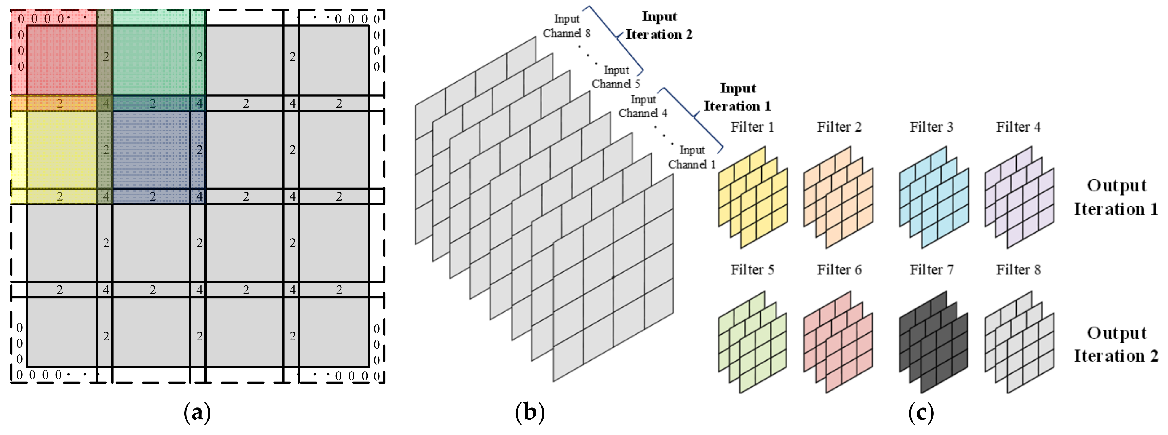
The convolution operation with a 6 × 6 kernel is performed by executing the convolution operation with a 3 × 3 kernel on the KU. Figure 7 illustrates the segmentation of a convolution operation using a 6 × 6 kernel into four 3 × 3 kernels for processing with the proposed design. In this mode, the input feature data for each convolution operation with a 3 × 3 kernel process a dedicated part of the whole input data, with overlapped contents. To calculate the final output of the convolution operation with a 6 × 6 kernel, we use a two-stage adder tree after finishing convolutions in the FDCAs.
4.6. Reconfigurable Input FIFO
Figure 8 shows the block diagram of the reconfigurable input FIFO. For each kernel mode, we utilize a portion of the reconfigurable input FIFO. Each FIFO stores one column of data for the input slice. Since each address of the FIFO contains four feature map data, the depth of the FIFO is equal to the slice size/4.
The following configurations of the reconfigurable input FIFO are used for different operation modes:
- The convolution operation with a 3 × 3 kernel and a stride of 1 requires the use of two SRAM-FIFOs and a register. While the KU reads data from the SRAM-FIFO or register, the data not only go to the KU but also to another SRAM-FIFO containing the previous data from the left column in the feature map.
- The convolution operation with a 3 × 3 kernel and a stride of 2 uses three SRAM-FIFOs. When the PEs array loads data from the FIFO address that stores the data for the last column, it also sends the data to another FIFO for reuse in the next first column, bypassing the middle column. This indicates that the stride 2 mode requires the KU to reuse only the data from the last column as the first column next time.
- The convolution operation with a 1 × 1 kernel and a stride of 1 only utilizes one SRAM-FIFO. In this mode, the output data only come from PE2.
4.7. FIFO Output Cache Memory
We used FIFO output cache memories to share feature map data between the input FIFO and KU. Each address in the input FIFO contains four feature map data at a moment. Therefore, the FIFO output cache memory block receives four data from FIFO at once, queues them in order, and transfers them to the KU, respectively. Each cache memory consists of eight 16-bit registers and enables the loading of one or two feature map data to the KU. We divided eight 16-bit registers into two parts, named Area0 and Area1, each consisting of four 16-bit registers.
In our design, we used a cache memory with depth = 8, which is twice the size of the data read from the FIFO. By using cache memory with eight registers, we will be able to read two data from the cache without waiting for the next four data from FIFO. In the case of using cache memory with depth = 4, it will not be possible to read and send two data to the KU at the same time.
For example, if we use cache memory with depth = 4, after reading three data from the cache memory, we would not be able to read another two data from it. We face a memory limitation problem in our circuit. If we read only one datum, which is left in the cache memory, then we must wait for the next four data readings from FIFO. This problem causes circuit insufficiency and produces incorrect output.
Figure 9 shows that the “finish” signal becomes active when reading data from a specific location in Area0 and Area1. For example, if the address is 2, then finish[0] goes high when reading two data in Area0. The “finish” signal acts as the read enable signal for the input FIFO and generates the write enable signal for the FIFO output cache memory via a register. When data are initially stored in the FIFO output cache memory, the finish signal cannot be activated until the data are read from the FIFO output cache memory. Therefore, the cache memory must read data from the FIFO using the init_rd_en signal generated by the controller.
4.8. Slice and Iteration
Modern CNN models are becoming increasingly complex by using large image sizes for input data and increasing the depth and scale of neural networks to achieve high prediction accuracy. Due to these changes in CNN models, there is a need to develop new hardware accelerator models with high processing capabilities and reconfigurability. This work introduces the concept of slicing, which involves uniformly cutting a whole input feature map into specific-sized parts. The concept of slicing is not only used for defining the height and width of each slice but also the depth of the input channel, which is divided into slices based on the number of input channels.
After applying the slicing of the input data, each slice must be processed separately with filters. It is determined by the number of iterations required to process the entire input data. In our design, we introduced and used new-iteration ideas, such as input, slice, and output iteration, to process the input data efficiently and quickly.
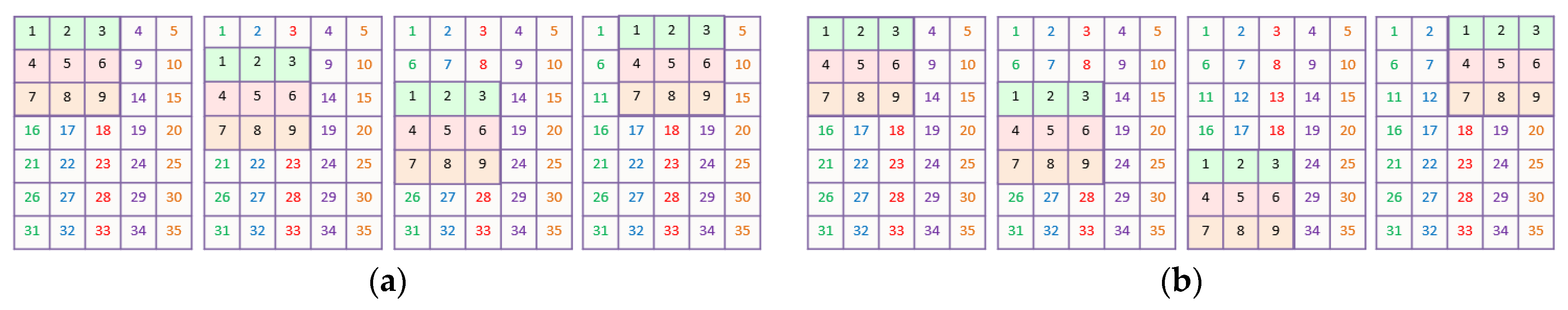
By applying the concept of slicing, we reduce the amount of input data needed for processing in the CNN accelerator at once. As a result, the size of the on-chip memory and computational circuits is effectively reduced. To achieve the aforementioned improvements, this study not only introduced the concept of slicing but also implemented the idea for a limited number of kernels. Figure 10 illustrates how the iteration is defined in our architecture based on the feature map size and slice. When using the concept of slicing in convolution, there is an overlap between two slices. Figure 10a shows that the overlap between slices occurs when using 3 × 3 kernels. Figure 10b,c represent an example of input/output iteration. In this study, because 16 input channels and 8 filters can be used for calculation simultaneously, the number of channels used for one input iteration becomes 16, contrary to what is shown in the figure. Similarly, eight (8) filters are used for convolution processing in each output iteration.
4.9. Input Padding
To add padding to the input feature map, most CNN accelerators use a software-based approach before loading the data to the DDR DRAM. In this work, we designed the circuit to add zero padding around the input feature map, a concept known as input padding in the circuit. Using input padding is more effective than using output padding. Figure 11 presents the ratio of input padding storage pixels to output padding based on the size of the input feature map. The figure shows that as the feature map size decreases, the proportion of storage pixels also decreases by up to 82.6%.
The input padding circuit includes the register and control signal. The first component is the 2-bit padding state register, known as the “FIFO write selection”, which varies depending on the current/total slice iteration and kernel mode (Figure 12). Table 1 and Figure 13, along with the description below, explain the adding-zero-padding method for each case.
- ZEROZERO: When all data entering the reconfigurable FIFO is zero, only zeros are needed for padding.
- READZERO: All data from the global input buffer are loaded into the FIFO when the slice iteration does not require any padding.
- ZEROREAD: All data in the global input buffer are loaded, and a single zero is inserted in front of the data as padding. It is used to load a part of the zero padding at the top slice of the input feature map.
- SHIFTREAD: When importing new data, the last pixel of the previously imported data is concatenated with the newly read data. The function exists to use the most recently imported data in the ZEROREAD scenario.
The 1-bit wire, InB_flag, generates a read enable signal for the global input buffer by entering a two-input AND gate with a read enable signal asserted by the controller in the KU. If the “FIFO write selection” is ZEROZERO, then the wire has a value of 0, and the KU receives only a “zero” value for the padding. Therefore, KU receives “zero” data without accessing the global input buffer.
The kernel mode also affects padding. The 3 × 3 convolution operation with a stride of 1 requires adding zeros around all sides of the input feature map. For a stride of 2, additional zeros are only required for the upper and left sides of the input. Padding is not applied in a 1 × 1 convolution operation.
4.10. Bias–Activation–Scaling Pipeline Architecture
In this study, we targeted the YOLOv5n model and quantized the model to an integer representation. Thus, we designed an extra circuit to calculate bias, activation, and scaling parameters for converting the final convolution result into the feature map for the next layer. Figure 14 illustrates the bias–activation–scaling (BAS) pipeline architecture used in the proposed SoC hardware. All parameters, bias, activation, and scaling parameters are represented as 16-bit integers, allowing for a fast and low-cost area architecture. The pipeline process consists of six stages and requires seven cycles to process one piece of data.
The bias is seen as a part of batch normalization (BN). BN is usually used to train CNN models. In YOLOv5 training, the BN for CNN layers is calculated using Equation (2):
Here, the is the output of convolutional filter, represents the mean, means the variance, epsilon () is added for numerical stability, is the batch normalization scaling factor, and is the shift factor (bias). These parameters are determined during the training process, and they remain constant within each layer during the inference [14,28,29,31].
The convolution operation with bias can be represented by the following equation:
where represents weight, is input feature map, and means the constant number called “bias”. We simplify the addition in Equation (2) as Equation (3). This simplification reduces hardware costs without sacrificing accuracy. In addition, we used techniques like rounding and truncation in the BAS circuit.
The 36-bit dividers are used in the Leaky ReLU activation circuit, and they require two clock cycles to prevent setup-time violations at a high frequency of 400 MHz. The scaling process consists of four stages and operates for four cycles. The process involves multiplication, division, rounding, addition, truncation, and subtraction, in that order. The scaling applies the parameters generated by quantization.
5. Advantage of the Proposed Architecture
The YOLOv5n model requires numerous computations for each layer, with almost 99% of them involving the convolution operation. Therefore, we developed a reconfigurable and optimized hardware accelerator for convolution operations. The proposed computing method in the CNN accelerator supports stride 1 and stride 2 convolution operations with various kernel sizes. It enhances computational efficiency by using slicing and iterations, thereby accelerating image processing in hardware. Our design efficiently utilizes hardware resources to perform fast convolution operations, offering numerous structural advantages. In this section, we will discuss the improvements in the proposed architecture.
5.1. High PE Array Utilization with Flexibility
Most CNN accelerator architectures demonstrate good resource utilization, reaching up to 90% in commonly used kernel modes [3,28]. Due to CNN models becoming more complex by increasing the depth and scale of deep neural networks (DNNs) and using different kernel sizes and striding for image processing, they cannot perform all necessary convolution operations. Traditional CNN accelerators typically only operate with a kernel size of 3 × 3 and a stride of 1 or they may support a stride of 2 with less than 25% utilization. Therefore, we designed a new CNN accelerator architecture with FDCA to efficiently perform convolution operations using newly introduced kernel modes. Our proposed architecture demonstrates that PE resource utilization exceeds 95%, even for convolutions with kernel sizes of 3 × 3 or 6 × 6 at a stride of 2. Table 2 presents the PE utilization ratio for various kernel modes with a slice size of 160.
5.2. Convolution Operation 3 × 3 Stride 2 Speed Optimization
Table 3 presents a comparison of the clock cycles required for 3 × 3 convolution with a stride of 2 in the previous and proposed architectures for processing the YOLOv5n model. The proposed architecture consumes about 9.4-times-fewer clock cycles. The proposed architecture provided more data in the same time frame for the speed optimization of convolution operation with 3 × 3 stride 2.
5.3. Area Efficiency
In general, the optimized architecture for the specific kernel (size) mode demonstrates high PE utilization. However, designing individual sub-circuits for each kernel mode requires a significant amount of hardware resources. Therefore, in our proposed CNN accelerator, we have designed it so that more than 90% of the KU area is shared among all kernel modes. The multiplexer (Mux) is used to configure the connection between the PEs of the KU for the required kernel mode.
Table 4 presents the total number of logic gates for the proposed CNN architecture and previous architectures in different kernel modes. It shows that the proposed architecture’s area is 2.14 times smaller than the total area of the previous architecture. The area was reduced to 2.14 times instead of 3 times due to the convolution operation with a 1 × 1 kernel mode, which utilizes only one PE, but the total area of KU is still 9 times larger.
Although the proposed architecture supports two additional kernel modes, the total chip area increases by only 6% compared to using the predicted 3 × 3 stride 1 mode separately. If we expand the proposed CNN accelerator architecture to support 6 × 6 convolution operations with stride 1 and stride 2 modes in the future, the expected chip area will increase by 6% compared to the current area.
5.4. Data Load Optimization
The proposed design significantly improves data loading speed, performing nine times faster than a GPU. In our design, we efficiently utilized the following components to achieve faster data loading on the circuit:
- We used reconfigurable input FIFOs to organize, transfer, and reuse data on the KU. FIFOs manage all data feeding and reusing procedures on the vertical and horizontal lines of the KU unit during convolution operations. Our design allows for the use of up to three FIFOs, depending on the configuration of the KU (PEs array). Because of these three reconfigurable input FIFOs, the KU can reuse feature map data, reducing the number of data loads by up to one-third.
- The KU reuses data by sharing them among connected PEs. Typically, the GPU reads each pixel of input data from DDR memory three times. In our design, the KU reuses the same pixel data three times by passing it to other PEs. This mechanism reduces the number of memory accesses by three times.
5.5. Small On-Chip Memory Size
Each of the four FDCAs consists of 32 KUs. Each FDCA is designed to simultaneously compute four input and eight output channels. The overall design supports the computing of 16 parallel input channels by employing four FDCAs in a parallel architecture. This allows for the simultaneous processing of data from 16 (sixteen) input feature map channels.
Modern CNN models, such as the YOLOv5n used in this study, require the processing of more than sixteen input and output data channels during convolutional layer computation. Simultaneously processing all corresponding channels in parallel requires multiple connected PE arrays and on-chip memories, which increases the hardware costs of the CNN accelerator by occupying a large amount of hardware resources. Therefore, we applied the slicing and iteration concepts to efficiently process the input data. As a result, we were able to optimize power consumption and chip area utilization.
By using the concept of slicing, we convolve a part of the input feature map with given filters to generate the sliced output result. In this scenario, only the essential slice data will be copied from DDR memory for processing in the FDCA block. Therefore, the proposed architecture stores partial input feature map data corresponding to a single slice, and it uses a smaller on-chip memory size in the design compared to storing the entire feature map. Utilizing small on-chip memories helps to minimize the number of accesses to the DDR memory, reduce data loading time, and maximize data reuse in slice rotating operations, which involve reusing the same data for different filter weights.
6. Hardware Implementation Results
In order to evaluate the hardware cost of the proposed CNN accelerator, we implemented it on the Xilinx Zynq UltraScale+ MPSoC ZCU102 FPGA platform. For hardware synthesis, Vivado 2022.2 is used. Our implementation occupies 249,357 LUTs, 2304 DSPs, and 567 KB of BRAMs in FPGA resource utilization. The CNN accelerator operates at 400 MHz, and the reference image inference speed is 47.17 frames per second (FPS). Table 5 shows the implementation results on FPGA.
To test the performance of the proposed CNN accelerator, we accelerated a quantized YOLOv5n model for inference. For this purpose, we have developed a microcode-based CNN controller circuit that allows for the programmability of any CNN model. Our modified YOLOv5n is an object detection model pre-trained on the COCO dataset. All model parameters, including weights, bias values, and input feature map data, were quantized to 8-bit integers. The model’s object detection performance was evaluated using mean average precision (mAP). We set our threshold at 0.5 ([email protected]) and achieved a detection mAP of 43.1% on the FPGA. The results demonstrate that the proposed architecture implementation significantly improves inference throughput while maintaining high accuracy, similar to the software model.
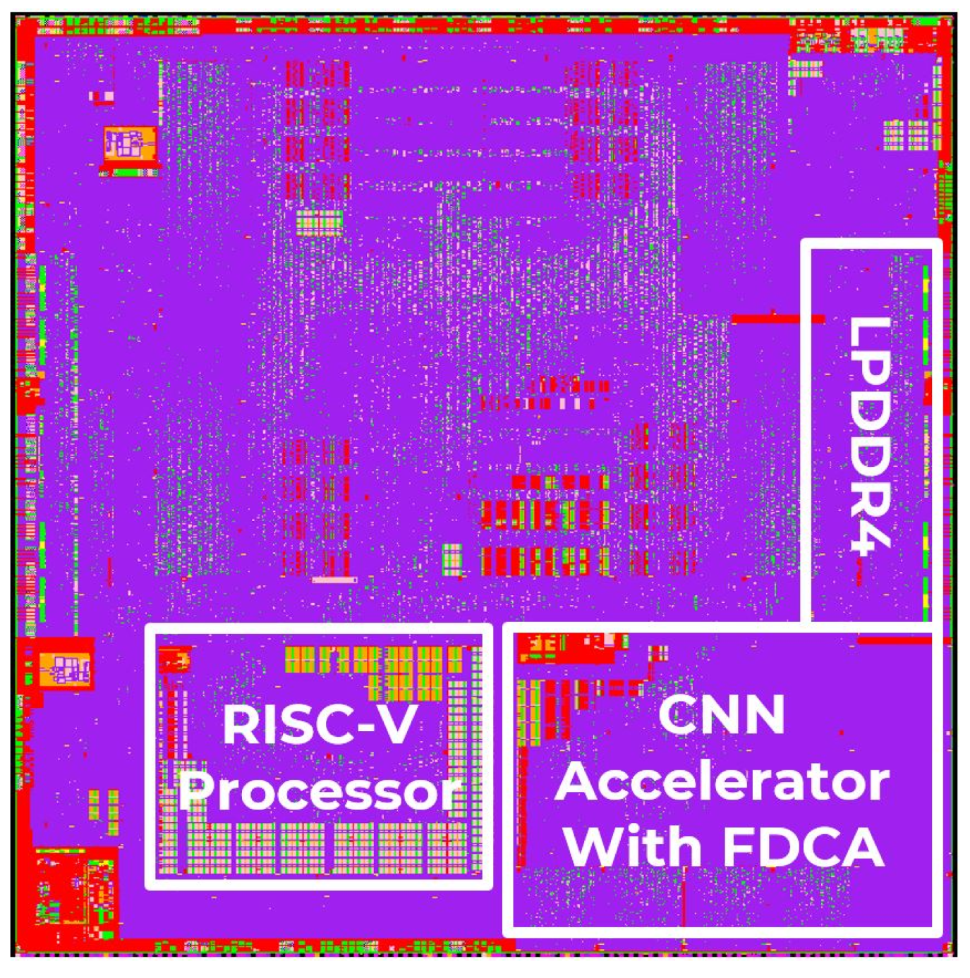
Furthermore, the proposed CNN accelerator was implemented as a system on chip (SoC) using a Samsung 14 nm CMOS process. The die consists of a shared LPDDR, RISC-V core, and CNN accelerator with FDCA, which are utilized in collaboration with partner companies. The area allocated for the CNN accelerator architecture is 10.96 mm2 (3943 µm × 2780 µm). The chip operates at a frequency of 400 MHz, with a timing constraint set at 2.5 ns. The total power consumption of the chip is 18.52 mW. The implementation uses on-chip SRAM with a size of 275.75 KB. Figure 15 shows the overall chip layout of the proposed CNN accelerator SoC.
7. Conclusions
In this paper, we proposed a high-speed CNN accelerator architecture based on a flexible diagonal cyclic array (FDCA). The proposed four-FDCA architecture comprises 1152 PEs that can process the data for sixteen input channels and eight output channels simultaneously. The proposed architecture enables the execution of convolution operations with different kernel modes and strides to accelerate the latest CNN models. In the proposed design, we introduced new optimization techniques that improved chip area efficiency by 6% and reduced total chip area utilization by 2.14 times compared to individual block designs for each kernel mode. We also minimized the number of DRAM accesses by using data reuse methods.
The CNN accelerator was synthesized and verified on the Xilinx ZCU102 FPGA and implemented in SoC silicon using 14 nm CMOS process technology. The results demonstrate that the proposed CNN accelerator can perform convolution operations 3.8 times faster, using the proposed new PE array structure, compared to previous CNN accelerators.
Author Contributions
Conceptualization, D.-Y.L., H.A. and H.-W.K.; Designing, D.-Y.L. and H.A.; verification, M.J.; validation, S.-B.P. and M.J.; formal analysis H.A. and D.-Y.L.; writing—original draft preparation D.-Y.L.; writing—review and editing, H.A. and S.-B.P.; funding, S.-H.S. and K.-M.L. All authors have read and agreed to the published version of the manuscript.
Funding
This work was supported by the National Research Foundation of Korea (NRF) grant for RLRC funded by the Korea government (MSIT) (No. 2022R1A5A8026986, RLRC, 25%), and was also supported by the Institute of Information and communications Technology Planning and Evaluation (IITP) grant funded by the Korea government (MSIT) (No. 2020-0-01304, Development of Self-Learnable Mobile Recursive Neural Network Processor Technology, 25%). It was partly supported by Innovative Human Resource Development for Local Intellectualization program through the Institute of Information & Communications Technology Planning & Evaluation (IITP) grant funded by the Korea government (MSIT) (IITP-2024-2020-0-01462, 25%). The National R&D Program supported this research through the National Research Foundation of Korea (NRF) funded by the Ministry of Science and ICT (No. 2020M3H2A1076786, System Semiconductor specialist nurturing, 25%).
Data Availability Statement
Data are contained within the article.
Acknowledgments
We thank Thaising Thaing ([email protected]) for his invaluable contributions to this work.
Conflicts of Interest
The authors declare no conflicts of interest.
References
- Akkad, G.; Mansour, A.; Inaty, E. Embedded Deep Learning Accelerators: A Survey on Recent Advances. IEEE Trans. Artif. Intell. 2023; early access. [Google Scholar]
- Jocher, G.; Stoken, A.; Chaurasia, A.; Borovec, J.; Xie, T.; Kwon, Y.; Michael, K.; Changyu, L.; Fang, J. Yolov5. NanoCode012. v6.0—Models. 2021. Available online: https://github.com/ultralytics/yolov5 (accessed on 12 October 2021).
- Huang, W.; Wu, H.; Chen, Q.; Luo, C.; Zeng, S.; Li, T.; Huang, Y. FPGA-Based High-Throughput CNN Hardware Accelerator with High Computing Resource Utilization Ratio. IEEE Trans. Neural Netw. Learn. Syst. 2022, 33, 4069–4083. [Google Scholar] [CrossRef] [PubMed]
- Yang, J.; Fu, W.; Cheng, X.; Ye, X.; Dai, P.; Zhao, W. S2 Engine: A Novel Systolic Architecture for Sparse Convolutional Neural Networks. IEEE Trans. Comput. 2022, 71, 1440–1452. [Google Scholar]
- Wei, X.; Yu, C.H.; Zhang, P.; Chen, Y.; Wang, Y.; Hu, H.; Liang, Y.; Cong, J. Automated systolic array architecture synthesis for high throughput CNN inference on FPGAs. In Proceedings of the 2017 54th ACM/EDAC/IEEE Design Automation Conference (DAC), Austin, TX, USA, 18–22 June 2017; pp. 1–6. [Google Scholar]
- Andri, R.; Cavigelli, L.; Rossi, D.; Benini, L. Hyperdrive: A Multi-Chip Systolically Scalable Binary-Weight CNN Inference Engine. IEEE J. Emerg. Sel. Top. Circuits Syst. 2019, 9, 309–322. [Google Scholar] [CrossRef]
- Sedukhin, S.; Tomioka, Y.; Yamamoto, K. In search of the performance-and energy-efficient CNN accelerators. IEICE Trans. Electron. 2022, 105, 209–221. [Google Scholar] [CrossRef]
- Liu, C.-N.; Lai, Y.-A.; Kuo, C.-H.; Zhan, S.-A. Design of 2D Systolic Array Accelerator for Quantized Convolutional Neural Networks. In Proceedings of the 2021 International Symposium on VLSI Design, Automation and Test (VLSI-DAT), Hsinchu, Taiwan, 19–22 April 2021; pp. 1–4. [Google Scholar]
- Jouppi, N.P.; Young, C.; Patil, N.; Patterson, D.; Agrawal, G.; Bajwa, R.; Bates, S.; Bhatia, S.; Boden, N.; Borchers, A.; et al. In-datacenter performance analysis of a tensor processing unit. In Proceedings of the 2017 ACM/IEEE 44th Annual International Symposium on Computer Architecture (ISCA), Toronto, ON, Canada, 24–28 June 2017; pp. 1–12. [Google Scholar]
- Wang, Y.; Wang, Y.; Shi, C.; Cheng, L.; Li, H.; Li, X. An Edge 3D CNN Accelerator for Low-Power Activity Recognition. IEEE Trans. Comput. Aided Des. Integr. Circuits Syst. 2021, 40, 918–930. [Google Scholar] [CrossRef]
- Parmar, Y.; Sridharan, K. A Resource-Efficient Multiplierless Systolic Array Architecture for Convolutions in Deep Networks. IEEE Trans. Circuits Syst. II Express Briefs 2020, 67, 370–374. [Google Scholar] [CrossRef]
- Chen, Y.-H.; Krishna, T.; Emer, J.S.; Sze, V. Eyeriss: An Energy-Efficient Reconfigurable Accelerator for Deep Convolutional Neural Networks. IEEE J. Solid-State Circuits 2017, 52, 127–138. [Google Scholar] [CrossRef]
- Lu, Y.C.; Chen, C.W.; Pu, C.C.; Lin, Y.T.; Jhan, J.K.; Liang, S.P. Live Demo: An 176.3 GOPs Object Detection CNN Accelerator Emulated in a 28 nm CMOS Technology. In Proceedings of the 2021 IEEE 3rd International Conference on Artificial Intelligence Circuits and Systems (AICAS), Washington, DC, USA, 6–9 June 2021; pp. 1–4. [Google Scholar]
- Nguyen, D.T.; Nguyen, T.N.; Kim, H.; Lee, H.J. A High-Throughput and Power-Efficient FPGA Implementation of YOLO CNN for Object Detection. IEEE Trans. Very Large Scale Integr. (VLSI) Syst. 2019, 27, 1861–1873. [Google Scholar] [CrossRef]
- Yepez, J.; Ko, S.-B. Stride 2 1-D, 2-D, and 3-D Winograd for Convolutional Neural Networks. IEEE Trans. Very Large Scale Integr. (VLSI) Syst. 2020, 28, 853–863. [Google Scholar] [CrossRef]
- Li, Y.; Lu, S.; Luo, J.; Pang, W.; Liu, H. High-performance Convolutional Neural Network Accelerator Based on Systolic Arrays and Quantization. In Proceedings of the 2019 IEEE 4th International Conference on Signal and Image Processing (ICSIP), Wuxi, China, 19–21 July 2019; pp. 335–339. [Google Scholar]
- Yang, G.; Lei, J.; Xie, W.; Fang, Z.; Li, Y.; Wang, J.; Zhang, X. Algorithm/Hardware Codesign for Real-Time On-Satellite CNN-Based Ship Detection in SAR Imagery. IEEE Trans. Geosci. Remote Sens. 2022, 60, 5226018. [Google Scholar] [CrossRef]
- Ansari, A.; Ogunfunmi, T. Hardware Acceleration of a Generalized Fast2-D Convolution Method for Deep Neural Networks. IEEE Access 2022, 10, 16843–16858. [Google Scholar] [CrossRef]
- Yan, T.; Zhang, N.; Li, J.; Liu, W.; Chen, H. Automatic Deployment of Convolutional Neural Networks on FPGA for Spaceborne Remote Sensing Application. Remote Sens. 2022, 14, 3130. [Google Scholar] [CrossRef]
- Ardakani, A.; Condo, C.; Ahmadi, M.; Gross, W.J. An Architecture to Accelerate Convolution in Deep Neural Networks. IEEE Trans. Circuits Syst. I Regul. Pap. 2018, 65, 1349–1362. [Google Scholar] [CrossRef]
- Wang, J.; Yuan, Z.; Liu, R.; Feng, X.; Du, L.; Yang, H.; Liu, Y. GAAS: An Efficient Group Associated Architecture and Scheduler Module for Sparse CNN Accelerators. IEEE Trans. Comput. Aided Des. Integr. Circuits Syst. 2020, 39, 5170–5182. [Google Scholar] [CrossRef]
- Wang, J.; Park, S.; Park, C.S. Spatial Data Dependence Graph Based Pre-RTL Simulator for Convolutional Neural Network Dataflows. IEEE Access 2022, 10, 11382–11403. [Google Scholar] [CrossRef]
- Li, J.; Un, K.-F.; Yu, W.-H.; Mak, P.-I.; Martins, R.P. An FPGA-Based Energy-Efficient Reconfigurable Convolutional Neural Network Accelerator for Object Recognition Applications. IEEE Trans. Circuits Syst. II Express Briefs 2021, 68, 3143–3147. [Google Scholar] [CrossRef]
- Qiu, J.; Wang, J.; Yao, S.; Guo, K.; Li, B.; Zhou, E. Going deeper with embedded fpga platform for convolutional neural network. In Proceedings of the 2016 ACM/SIGDA International Symposium on Field-Programmable Gate Arrays, Monterey, CA, USA, 21–23 February 2016. [Google Scholar]
- Huan, Y.; Xu, J.; Zheng, L.; Tenhunen, H.; Zou, Z. A 3D Tiled Low Power Accelerator for Convolutional Neural Network. In Proceedings of the 2018 IEEE International Symposium on Circuits and Systems (ISCAS), Florence, Italy, 27–30 May 2018; pp. 1–5. [Google Scholar]
- Tu, F.; Yin, S.; Ouyang, P.; Tang, S.; Liu, L.; Wei, S. Deep Convolutional Neural Network Architecture with Reconfigurable Computation Patterns. IEEE Trans. Very Large Scale Integr. (VLSI) Syst. 2017, 25, 2220–2233. [Google Scholar] [CrossRef]
- Redmon, J.; Divvala, S.; Girshick, R.; Farhadi, A. You only look once: Unified, real-time object detection. In Proceedings of the 2016 IEEE Conference on Computer Vision and Pattern Recognition (CVPR), Las Vegas, NV, USA, 27–30 June 2016; pp. 779–788. [Google Scholar]
- Son, H.; Na, Y.; Kim, T.; Al-Hamid, A.A.; Kim, H. CNN Accelerator with Minimal On-Chip Memory Based on Hierarchical Array. In Proceedings of the 2021 18th International SoC Design Conference (ISOCC), Jeju Island, Republic of Korea, 6–9 October 2021; pp. 411–412. [Google Scholar]
- Zhang, S.; Cao, J.; Zhang, Q.; Zhang, Q.; Zhang, Y.; Wang, Y. An FPGA-Based Reconfigurable CNN Accelerator for YOLO. In Proceedings of the 2020 IEEE 3rd International Conference on Electronics Technology (ICET), Chengdu, China, 8–12 May 2020; pp. 74–78. [Google Scholar]
- Adiono, T.; Putra, A.; Sutisna, N.; Syafalni, I.; Mulyawan, R. Low Latency YOLOv3-Tiny Accelerator for Low-Cost FPGA Using General Matrix Multiplication Principle. IEEE Access 2021, 9, 141890–141913. [Google Scholar] [CrossRef]
- Li, P.; Che, C. Mapping YOLOv4-Tiny on FPGA-Based DNN Accelerator by Using Dynamic Fixed-Point Method. In Proceedings of the 2021 12th International Symposium on Parallel Architectures, Algorithms and Programming (PAAP), Xi’an, China, 10–12 December 2021; pp. 125–129. [Google Scholar]
- Babu, P.; Parthasarathy, E. Hardware acceleration for object detection using YOLOv4 algorithm on Xilinx Zynq platform. J. Real-Time Image Process. 2022, 19, 931–940. [Google Scholar] [CrossRef]
- Ma, Y.; Cao, Y.; Vrudhula, S.; Seo, J.-S. Optimizing the Convolution Operation to Accelerate Deep Neural Networks on FPGA. IEEE Trans. Very Large Scale Integr. (VLSI) Syst. 2018, 26, 1354–1367. [Google Scholar] [CrossRef]
- Zhang, C.; Sun, G.; Fang, Z.; Zhou, P.; Pan, P.; Cong, J. Caffeine: Toward Uniformed Representation and Acceleration for Deep Convolutional Neural Networks. IEEE Trans. Comput. Aided Des. Integr. Circuits Syst. 2019, 38, 2072–2085. [Google Scholar] [CrossRef]
Figure 1.
Processing element architecture.

Figure 2.
Proposed CNN accelerator architecture with RISC-V processor.

Figure 3.
Four-FDCA processing architecture block diagram.

Figure 4.
Kernel unit for convolution 3 × 3 stride 1.

Figure 5.
Kernel unit for convolution 3 × 3 stride 2.

Figure 6.
Example of filter shifting over the input feature map: (a) 3 × 3 stride 1; (b) 3 × 3 stride 2.
Figure 6.
Example of filter shifting over the input feature map: (a) 3 × 3 stride 1; (b) 3 × 3 stride 2.

Figure 7.
Applying 3 × 3 kernel mode for convolution operation with a 6 × 6 kernel.

Figure 8.
Reconfigurable input FIFO (red frame) with kernel unit.

Figure 9.
FIFO output cache memory.

Figure 10.
Concept of slice and iteration: (a) slice iteration and overlap (the color indicates the area of each slice, and the number indicates the overlap size.); (b) input iteration; (c) output iteration.
Figure 10.
Concept of slice and iteration: (a) slice iteration and overlap (the color indicates the area of each slice, and the number indicates the overlap size.); (b) input iteration; (c) output iteration.

Figure 11.
Input padding vs. output padding.

Figure 12.
Padding circuit structure.

Figure 13.
The use cases of a FIFO write select signal (number) depending on the padding position (red frame).
Figure 13.
The use cases of a FIFO write select signal (number) depending on the padding position (red frame).

Figure 14.
Bias–activation–scaling pipeline architecture: (a) bias; (b) activation (Leaky ReLU); (c) scaling.
Figure 14.
Bias–activation–scaling pipeline architecture: (a) bias; (b) activation (Leaky ReLU); (c) scaling.

Figure 15.
Full chip layout implemented in 14 nm CMOS process.


Table 1.
FIFO write selection signal states.
| FIFO Write Select | Reg0 | Reg1 | Reg2 | Reg3 | Reg4 |
|---|---|---|---|---|---|
| ① ZEROZERO | 0 | 0 | 0 | 0 | 0 |
| ② READZERO | InBuf[0] | InBuf[1] | InBuf[2] | InBuf[3] | 0 |
| ③ ZEROREAD | 0 | InBuf[0] | InBuf[1] | InBuf[2] | InBuf[3] |
| ④ SHIFTREAD | Reg4 | InBuf[0] | InBuf[1] | InBuf[2] | InBuf[3] |
Table 2.
Clock cycle and utilization according to kernel mode.
| Architecture | Kenel Mode | Clock Cycle (N) | Utilization (%) |
|---|---|---|---|
| Previous Architecture | 3 × 3 Stride 1 | 26,224 | 99.86 |
| 3 × 3 Stride 2 | 26,224 | 24.96 | |
| 1 × 1 Stride 1 | 25,609 | 11.11 | |
| Proposed Architecture | 3 × 3 Stride 1 | 26,015 | 99.98 |
| 3 × 3 Stride 2 | 6848 | 96.4 | |
| 1 × 1 Stride 1 | 25,611 | 11.11 | |
| Future Work | 6 × 6 Stride 2 | 6848 | 96.4 |
Table 3.
Comparison of stride-2-mode clock cycle.
| Layer | Previous (1DCA) [28] | Proposed (4FDCA) |
|---|---|---|
| Layer0 | 3,841,024 | 475,136 |
| Layer1 | 1,920,512 | 237,568 |
| Layer3 | 1,868,032 | 185,088 |
| Layer5 | 1,841,792 | 158,848 |
| Layer7 | 1,828,687 | 145,728 |
| Layer18 | 920,896 | 79,424 |
| Layer21 | 914,336 | 72,864 |
| Total | 13,135,264 | 1,354,656 |
| Clock Cycle Ratio | 9.39 | 1 |
Table 4.
Comparison of area using gate count number.
| Architecture | Kernel Mode | Gate Count Number |
|---|---|---|
| Application Using Previous Architecture [28] | 3 × 3 Stride 1 | 10,100,000 |
| 3 × 3 Stride 2 | 10,100,000 | |
| 1 × 1 Stride 1 | 2,700,000 | |
| Merge | 22,900,000 | |
| Proposed Architecture | 3 × 3 Stride 1 | 10,697,551 |
| 3 × 3 Stride 2 | ||
| 1 × 1 Stride 1 | ||
| Expanded Architecture | 6 × 6 stride 1, 2 | +200,000 |
Table 5.
FPGA implementation result.
| [14] | [29] | [31] | Proposed Architecture | |
|---|---|---|---|---|
| FPGA | VC707 | ZCU102 | Zynq-7020 | ZCU102 |
| LUT | 86k | 95k | 30.1k | 249k |
| DSP | 168 | 609 | 149 | 2304 |
| BRAM (kB) | 2308 | 2160 | 4731 | 567 |
| GOPs | 464.7 | 85.8 | - | 1075.2 |
| Parameter | Variable bit fixed point | 16-bit fixed point | 16-bit fixed point | 16-bit integer |
| Model | YOLOv2-tiny | YOLOv2-tiny | YOLOv4-tiny | YOLOv5n |
| CMOS chip SRAM (kB) | - | - | - | 275.75 |
Disclaimer/Publisher’s Note: The statements, opinions and data contained in all publications are solely those of the individual author(s) and contributor(s) and not of MDPI and/or the editor(s). MDPI and/or the editor(s) disclaim responsibility for any injury to people or property resulting from any ideas, methods, instructions or products referred to in the content. |
© 2024 by the authors. Licensee MDPI, Basel, Switzerland. This article is an open access article distributed under the terms and conditions of the Creative Commons Attribution (CC BY) license (https://creativecommons.org/licenses/by/4.0/).
Share and Cite
MDPI and ACS Style
Lee, D.-Y.; Aliev, H.; Junaid, M.; Park, S.-B.; Kim, H.-W.; Lee, K.-M.; Sim, S.-H. High-Speed CNN Accelerator SoC Design Based on a Flexible Diagonal Cyclic Array. Electronics 2024, 13, 1564. https://doi.org/10.3390/electronics13081564
AMA Style
Lee D-Y, Aliev H, Junaid M, Park S-B, Kim H-W, Lee K-M, Sim S-H. High-Speed CNN Accelerator SoC Design Based on a Flexible Diagonal Cyclic Array. Electronics. 2024; 13(8):1564. https://doi.org/10.3390/electronics13081564
Chicago/Turabian StyleLee, Dong-Yeong, Hayotjon Aliev, Muhammad Junaid, Sang-Bo Park, Hyung-Won Kim, Keon-Myung Lee, and Sang-Hoon Sim. 2024. "High-Speed CNN Accelerator SoC Design Based on a Flexible Diagonal Cyclic Array" Electronics 13, no. 8: 1564. https://doi.org/10.3390/electronics13081564
Note that from the first issue of 2016, this journal uses article numbers instead of page numbers. See further details here.