
Channel Potential of Bandgap-Engineered Tunneling Oxide (BE-TOX) in Inhibited 3D NAND Flash Memory Strings


1
Department of Electronics Engineering, Korea National University of Transportation, Room No. 326, Smart ICT Building, 50 Daehak-ro, Chungju-si 27469, Chungbuk, Republic of Korea
2
Semiconductor Devices and Circuits Laboratory, Advanced Institute of Convergence Technology (AICT), Seoul National University, 145, Gwanggyo-ro, Yeongtong-gu, Suwon-si 16229, Gyeonggi-do, Republic of Korea
*
Authors to whom correspondence should be addressed.
Electronics 2024, 13(8), 1573; https://doi.org/10.3390/electronics13081573
Submission received: 18 March 2024
/
Revised: 14 April 2024
/
Accepted: 19 April 2024
/
Published: 20 April 2024
Abstract
:In this study, the channel potential of inhibited strings in 3D NAND flash memory using a bandgap-engineered tunneling oxide (BE-TOX) structure is analyzed. The equivalent oxide thickness (EOT) of the structure using BE-TOX was designed to be the same as the conventional 3D NAND flash memory, and the channel potentials of the down coupling phenomenon (DCP) and natural local self-boosting (NLSB) effect were analyzed. As a result, the BE-TOX structure was confirmed to have a higher channel potential in the DCP and NLSB than the conventional structure, making it relatively effective for program disturbance. The main reason for the difference in the channel potential between the BE-TOX and conventional structures is that adjacent cells have different threshold voltages (Vth). When the same program voltage (VPGM) and program time (TPGM) were applied during the program operation, Vth decreased in the BE-TOX structure, which increased the channel potential when DCP and NLSB occurred. Finally, a simulation was conducted by varying the thicknesses of the oxide and nitride in the BE-TOX structure. Despite the EOT being fixed and the thicknesses of both nitride and oxide being varied, the channel potential was affected.
1. Introduction
Semiconductors have continually been developed to improve their density and performance. The conventional memory structure used to be 2D NAND flash; however, owing to structural limitations of being further scaled down, it was changed to 3D NAND flash memory [1,2,3,4,5,6]. However, the size of 3D NAND flash memory is also approaching its limit. To address these issues, alternative methods for improving the performance and increasing integration have been proposed. One such method involves modifying the device’s structure. For example, the bandgap-engineered tunneling oxide (BE-TOX) structure [7,8] has been reported to enhance key memory metrics such as fortifying device reliability and increasing speed. The BE-TOX structure has the advantage of a high erase speed through fast hole tunneling [9,10] and the suppression of direct tunneling in low electric fields by modifying the structure of the tunneling layer [11]. These advantages are characteristic of the selected strings. However, the current structure constitutes multiple strings that are extensively used; there exists an inhibited string that does not proceed with program operation. Analysis of the inhibited string is necessary because the channel is not directly connected to the body and can thus easily flow into a floating state, causing various phenomena [12,13,14,15]. Therefore, the analysis of the inhibited channel is as important as that of the selected string. During verify operation, the voltage of the Word Line (WL) decreases, the WL of the adjacent cell is turned off, and the channel changes to a floating state, resulting in a down coupling phenomenon (DCP) [16,17,18]. Subsequently, in program operation, electrons in the inhibited string channel are gathered in the selected WL channel while the program pulse is applied to the selected WL, resulting in natural local self-boosting (NLSB) [19,20]. DCP and NLSB must be analyzed because these phenomena occur in the inhibited string, causing channel potential changes and affecting program disturbances [21].
In this study, the channel potential of an inhibited string in a BE-TOX structure was analyzed. The analysis was conducted by comparing the DCP and NLSB channel potentials of the conventional and BE-TOX structures. In addition, the DCP and NLSB channel potentials were analyzed by varying the thicknesses of the oxide and nitride layers in the BE-TOX structure. The 3D technology computer-aided design (TCAD) tool, Sentaurus, was used to analyze the channel potential [22].
2. Conventional and BE-TOX Structures of 3D NAND Flash Memory
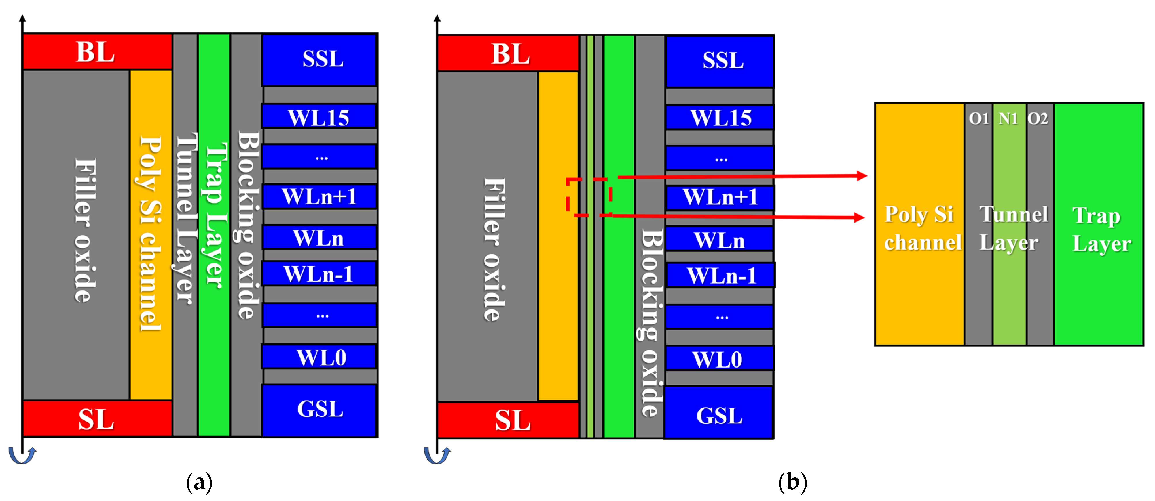
Figure 1a shows the structure of a conventional 3D NAND flash memory. This structure consists of a channel/tunneling layer (O)/trap layer (N)/blocking layer (O)/gate structure. Figure 1b shows a BE-TOX structure that was changed to a channel/tunneling layer (O1/N1/O2)/trap layer (N2)/blocking layer (O3)/gate by adding nitride to the tunneling layer, which only uses oxide in the structure shown in Figure 1a. Figure 1a,b show 16 WL (WL0–WL15), and the channel has a vertical structure. Because of its vertical structure, the channel is not directly connected to the body, which can otherwise lead to a floating state in the inhibited string [23,24,25].
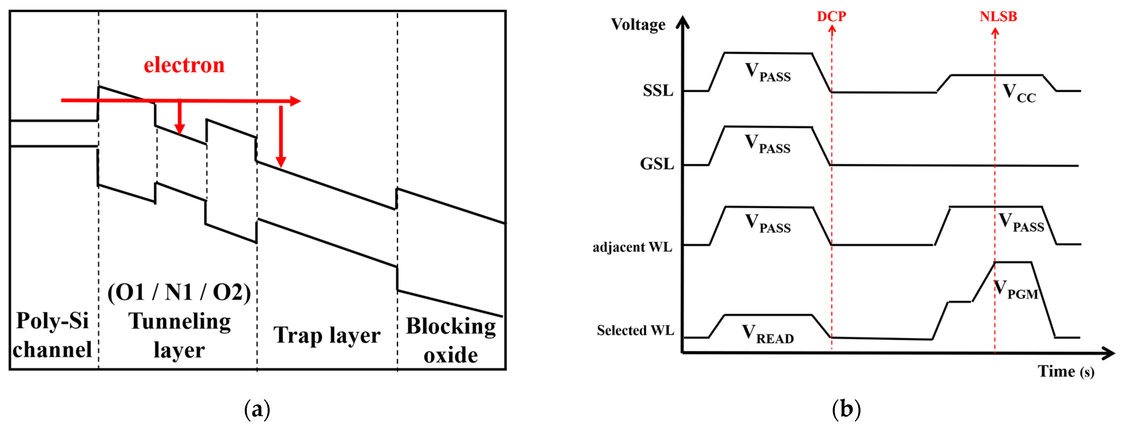
Table 1 presents a summary of the parameters of the 3D NAND flash memory and BE-TOX structure used in the simulation: gate length (WL), string select line (SSL), ground select line (GSL), gate spacing, gate dielectrics (O/N/O), channel hole diameter, and poly-Si channel thickness. In the BE-TOX structure, the thickness of the tunneling layer changed to O1 (1.5 nm)/N1 (1.9 nm)/O2 (1.5 nm). N1 was set to 1.9 nm to match the equivalent oxide thickness (EOT) with the conventional structure and because the nitride thickness of the trap layer should not exceed 2 nm. Subsequently, the EOT was fixed, even when the simulation was performed by varying the thicknesses of N1, O1, and O2 in the BE-TOX structure. Figure 2a shows a band diagram of BE-TOX structure during program operation. Figure 2b shows a timing diagram of the inhibited string simulation. To analyze DCP and NLSB in both structures, the voltage condition was changed and assumed to be an inhibited string and verify and program operations were performed. In the verify operation, all the WL voltages were applied to Vpass, and when the verify operation ended, the voltages were decreased to 0 V. At this point, the voltage of WL decreases, adjacent cells are turned off initially, and WL7 to WL9 change to a floating state. The phenomenon where the channel potential of the floating state decreases is called DCP. Subsequently, at the programming phase, the WL voltage was applied again. The channel maintains the floating state and increases the voltage of the selected WL. Electrons in the channel gather at the selected WL because of the potential difference, and the phenomenon where the channel potential of the selected WL exceeds that of the adjacent WL is called NLSB. In the inhibited string, the channel potential is related to the program disturbance. When the channel potential is high, the difference between the program voltage and the potential decreases, and unwanted programs can be prevented. For this reason, the higher the channel potential in DCP and NLSB, the lower the probability of program disturbance.
3. Results and Discussion
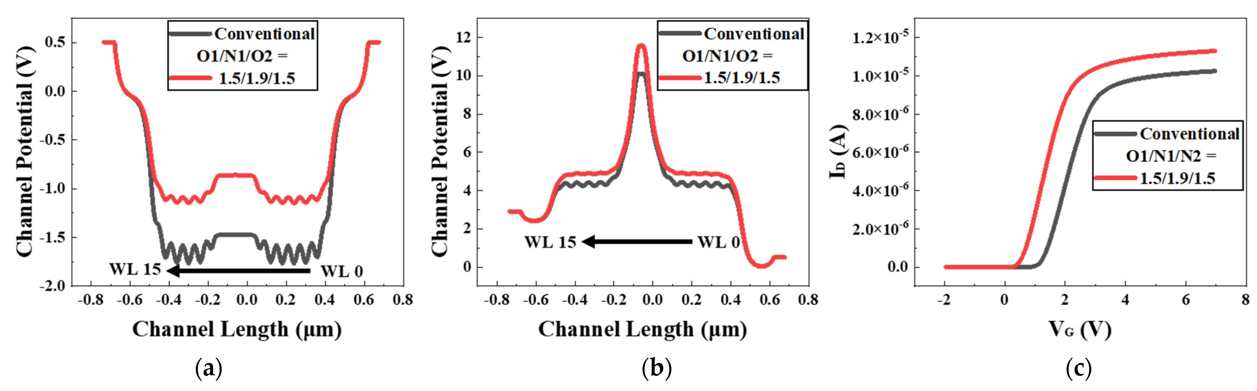
Figure 3 shows a graph comparing the conventional and BE-TOX structures of DCP and NLSB. As seen in the graph showing a comparison of DCP in Figure 3a, the channel potential of the BE-TOX structure was higher than the conventional structure. The NLSB is confirmed in Figure 3b, which shows that the channel potential of the BE-TOX structure is relatively high, making it more advantageous for program disturbances in inhibiting strings than the conventional structure. The primary reason underlying the difference in the DCP and NLSB of the channel potential is because of the variation in the Vth values of the adjacent cells. The graph in Figure 3c shows a comparison of the Vth values of the conventional and BE-TOX structures for adjacent cells. The program was executed using the same VPGM and TPGM as in the programming operation, the BE-TOX structure was found to have a lower Vth than the conventional structure. Additionally, to analyze the inhibited string channel potential of the BE-TOX structure more accurately, a simulation was conducted by fixing the EOT and changing the thicknesses of N1, O1, and O2 in the tunneling layer.
Figure 4 shows a graph of the same process obtained by fixing the tunneling oxide EOT thickness of the BE-TOX structure and adjusting the thicknesses of O1 and O2 according to the thickness of N1. Figure 4a,b show that the thickness of N1 affects the channel potential of the inhibited string. Figure 4a shows a DCP comparison graph for various N1 thicknesses and conventional structures. The channel potential was highest when the thickness of N1 was 1.5 nm. When the thickness of N1 decreased or increased from 1.5 nm, the channel potential decreased. Figure 4b shows an NLSB comparison graph for various N1 thicknesses and conventional structures. Similar to the DCP graph, Figure 4b shows that the channel potential was highest when the thickness of N1 was 1.5 nm. When the thickness of N1 decreased or increased from 1.5 nm, the channel potential decreased. Figure 4c shows the Vth comparison graph of adjacent cells for various N1 thicknesses and conventional structures. Vth was lowest when the thickness of N1 was 1.5 nm. When the thickness of N1 decreased or increased from 1.5 nm, Vt increased. As shown in Figure 4, when the thicknesses of N1 were 1.5 nm and 1.9 nm, DCP, NLSB, and Vth differed slightly. However, when the thickness of N1 was 1 nm, the difference increased because when the thickness of N1 is below a certain value, the device cannot be operated with BE-TOX. However, regardless of the N1 thickness of the BE-TOX structure, the channel potential was higher in both the DCP and NLSB structures than in the conventional structure, making it advantageous for program disturbance.
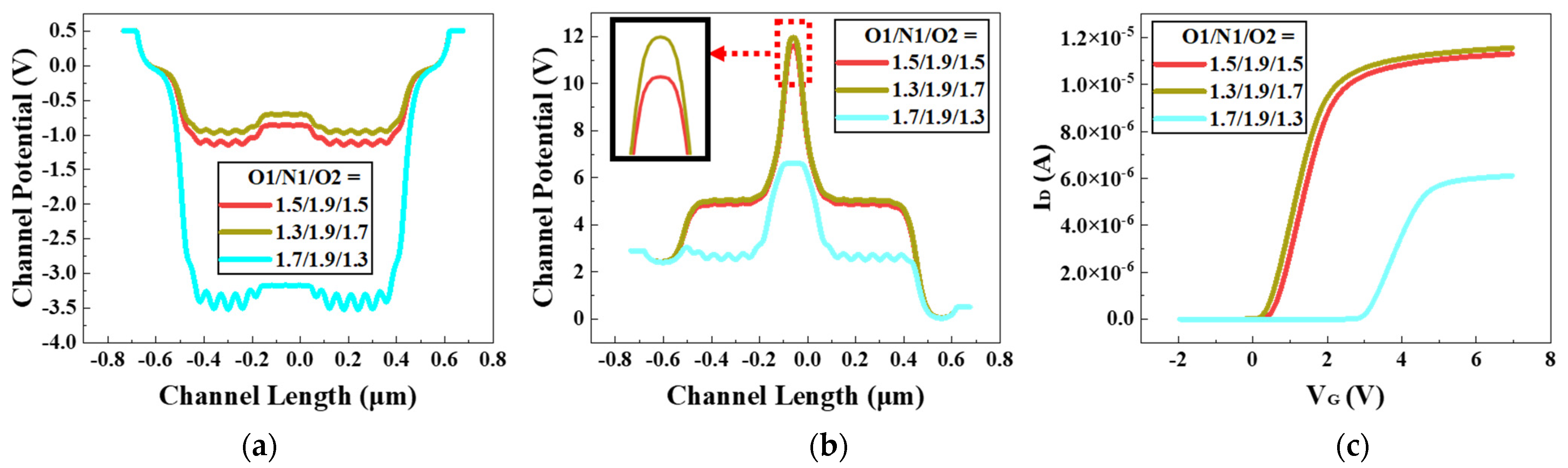
Figure 5 shows the results of the same process after fixing both the EOT and N1 thicknesses of the tunneling oxide and changing the thicknesses of O1 and O2. Figure 5a,b show that even when the EOT was fixed, the channel potential of the inhibited string was affected by the change in the oxide thickness. Figure 5a shows a DCP comparison graph of various O1 and O2 thicknesses. When the thickness of O1 increased and that of O2 decreased, the channel potential decreased. In other words, the channel potential increased when the thickness of O1 decreased and the thickness of O2 increased. Figure 5b is the NLSB comparison graph of various O1 and O2 thicknesses. Similar to the DCP graph, the thickness of O1 increases while that of O2 decreases, and the channel potential decreases. Figure 5c shows the adjacent cell Vth comparison graph for various O1 and O2 thicknesses. Figure 5c shows that when the thickness of O1 increases and that of O2 decreases, Vt increases. Figure 4 and Figure 5 reveal that the difference in Vth significantly affects the channel potential of the inhibited string, and it can be seen that even if the EOT is fixed, the channel potential of the inhibited string is affected by the thickness change in N1, O1, and O2.
4. Conclusions
In this study, the channel potential of the inhibited string of the BE-TOX structure was analyzed. The EOT values of both structures were equal. The same VPGM and TPGM were applied, and the program operation was performed on adjacent cells, except for WL7–WL9. Subsequently, the string state was inhibited, and the verify operation and program operation were conducted to confirm the channel potential in the DCP and NLSB. Therefore, the BE-TOX structure had higher channel potentials for both DCP and NLSB than the conventional structure. In addition, simulations were conducted while fixing the EOT of the BE-TOX structure and varying the thicknesses of N1, O1, and O2. The channel potentials of the DCP and NLSB were the highest when the thickness of N1 was 1.5 nm. When the thickness of N1 decreased or increased from 1.5 nm, the channel potential decreased. However, regardless of the thickness of N1, the BE-TOX structure had a higher channel potential of the DCP and NLSB than the conventional structure, making it advantageous for program disturbance. Finally, a simulation was conducted by fixing the thicknesses of both the EOT and N1 and adjusting the O1 and O2 thicknesses of the tunneling layer. When the thickness of O1 was increased and the thickness of O2 decreased, the channel potentials of the DCP and NLSB decreased. The channel potentials of the DCP and NLSB were correlated with the Vth values of the adjacent cells. The higher the Vth, the lower the DCP and NLSB channel potentials, and the lower the Vth, the higher the channel potentials of the DCP and NLSB. A higher channel potential results in a lower probability of program disturbances in the inhibited string, which is another advantage of the BE-TOX structure.
Author Contributions
Conceptualization, data curation, formal analysis, investigation, methodology, project administration, software (sentaurus version T-2022.03), validation, writing—original draft, T.C.; writing—original draft, writing—review and editing, validation, visualization, S.J.; funding acquisition, investigation, writing—review and editing, resources, software (sentaurus version T-2022.03), supervision, validation, visualization, writing—original draft, M.K. All authors have read and agreed to the published version of the manuscript.
Funding
This research was supported by the National R&D Program through the National Research Foundation of Korea (NRF) funded by the Ministry of Science and ICT of Korea (MSIT) (RS-2023-00258527).
Data Availability Statement
Data are contained within the article.
Conflicts of Interest
The authors declare no conflicts of interest.
References
- Kim, H.; Ahn, S.-J.; Shin, Y.G.; Lee, K.; Jung, E. Evolution of NAND flash memory: From 2D to 3D as a storage market leader. In Proceedings of the IEEE Int. Memory Workshop, Monterey, CA, USA, 14–17 May 2017; pp. 1–4. [Google Scholar] [CrossRef]
- Choi, E.-S.; Park, S.-K. Device considerations for high density and highly reliable 3D NAND flash cell in near future. In Proceedings of the 2012 International Electron Devices Meeting, San Francisco, CA, USA, 10–13 December 2012; pp. 9.4.1–9.4.4. [Google Scholar] [CrossRef]
- Ouyang, Y.; Xia, Z.; Yang, T.; Shi, D.; Zhou, W.; Huo, Z. Optimization of performance and reliability in 3D NAND flash memory. IEEE Electron Device Lett. 2020, 41, 840–843. [Google Scholar] [CrossRef]
- Choi, Y.-J.; Suh, K.-D.; Koh, Y.-N.; Park, J.-W.; Lee, K.-J.; Cho, Y.-J.; Suh, B.-H. A highspeed programming scheme for multi-level NAND flash memory. In Proceedings of the 1996 Symposium on VLSI Circuits, Digest of Technical Papers, Honolulu, HI, USA, 13–15 June 1996. [Google Scholar] [CrossRef]
- Takeuchi, K.; Tanaka, T.; Tanzawa, T. A multipage cell architecture for high-speed programming multilevel NAND flash memories. IEEE J. Solid-State Circuits 1998, 33, 1228–1238. [Google Scholar] [CrossRef]
- Takeuchi, K. Novel Co-Design of NAND Flash Memory and NAND Flash Controller Circuits for Sub-30 nm Low-Power High-Speed Solid-State Drives (SSD). IEEE J. Solid-State Circuits 2009, 44, 1227–1234. [Google Scholar] [CrossRef]
- Kim, M.; Shin, H. Analysis and compact modeling of fast detrapping from bandgap-engineered tunneling oxide in 3-D NAND flash memories. IEEE Trans. Electron Devices 2021, 68, 3339–3345. [Google Scholar] [CrossRef]
- Lue, H.-T.; Lai, S.-C.; Hsu, T.-H.; Du, P.-Y.; Wang, S.-Y.; Hsieh, K.-Y.; Liu, R.; Lu, C.-Y. Modeling of barrier-engineered charge-trapping NAND flash devices. IEEE Trans. Device Mater. Rel. 2010, 10, 222–232. [Google Scholar] [CrossRef]
- Wang, S.-Y.; Lue, H.-T.; Du, P.-Y.; Liao, C.-W.; Lai, E.-K.; Lai, S.-C.; Yang, L.-W.; Yang, T.; Chen, K.-C.; Gong, J.; et al. Reliability and processing effects of bandgap-engineered SONOS (BE-SONOS) flash memory and study of the gate-stack scaling capability. IEEE Trans. Device Mater. Rel. 2008, 8, 416–425. [Google Scholar] [CrossRef]
- Choi, N.; Kang, H.-J.; Bae, J.-H.; Park, B.-G.; Lee, J.-H. Effect of nitrogen content in tunneling dielectric on cell properties of 3-D NAND flash cells. IEEE Electron Device Lett. 2019, 40, 702–705. [Google Scholar] [CrossRef]
- Lue, H.-T.; Wang, S.-Y.; Lai, E.-K.; Shih, Y.-H.; Lai, S.-C.; Yang, L.-W.; Chen, K.-C.; Ku, J.; Hsieh, K.-Y.; Liu, R.; et al. BE-SONOS: A bandgap engineered SONOS with excellent performance and reliability. In Proceedings of the IEEE InternationalElectron Devices Meeting, New York, NY, USA, 5 December 2005; pp. 555–558. [Google Scholar] [CrossRef]
- Kim, H.; Kang, M. Analysis of DCP and NLSB Recovery Time in 3D NAND Flash Memory. Knut Dcollection. February 2023. Available online: http://www.dcollection.net/handler/chains/200000667859 (accessed on 3 February 2024).
- Ham, I.; Jeong, Y.; Baik, S.J.; Kang, M. Ferroelectric polarization aided low voltage operation of 3D NAND flash memories. Electronics 2020, 10, 38. [Google Scholar] [CrossRef]
- Jang, J.; Kim, H.S.; Cho, W.; Cho, H.; Kim, J.; Shim, S.I.; Jang, Y.; Jeong, J.H.; Son, B.K.; Kim, D.W.; et al. Vertical cell array using TCAT(Terabit Cell Array Transistor) technology for ultra-high density NAND flash memory. In Proceedings of the 2009 Symposium on VLSI Technology, Kyoto, Japan, 15–17 June 2009; pp. 192–193. [Google Scholar] [CrossRef]
- Han, S.; Jeong, Y.; Jhon, H.; Kang, M. Investigation of inhibited channel potential of 3D NAND flash memory according to word-line location. Electronics 2020, 9, 268. [Google Scholar] [CrossRef]
- Kim, Y.; Kang, M. Down-coupling phenomenon of floating channel in 3D NAND flash memory. IEEE Electron Device Lett. 2016, 37, 1566–1569. [Google Scholar] [CrossRef]
- Ryu, G.; Kim, H.; Lee, J.; Kang, M. Analysis of channel potential recovery according to the back pattern in 3D NAND flash memory. Appl. Sci. 2023, 3, 7. [Google Scholar] [CrossRef]
- Giulianini, M.; Malavena, G.; Compagnoni, C.M.; Spinelli, A.S. Time Dynamics of the Down-Coupling Phenomenon in 3-D NAND Strings. IEEE Trans. Electron Devices 2022, 69, 6757–6762. [Google Scholar] [CrossRef]
- Kang, M.; Kim, Y. Natural local self-boosting effect in 3D NAND flash memory. IEEE Electron. Device Lett. 2017, 38, 1236–1239. [Google Scholar] [CrossRef]
- Cho, T.; Kim, H.; Kang, M. Inhibited channel potential of 3D NAND flash memory string according to transient time. Appl. Sci. 2023, 2, 24. [Google Scholar] [CrossRef]
- Kim, Y.; Kang, M. Predictive modeling of channel potential in 3-D NAND flash memory. IEEE Trans. Electron Devices 2014, 61, 3901–3904. [Google Scholar] [CrossRef]
- TCAD Sentaurus Device User Guide, Version 2015; Synopsys: Mountain View, CA, USA, 2015.
- Park, K.-T.; Nam, S.; Kim, D.; Kwak, P.; Lee, D.; Choi, Y.-H.; Choi, M.-H.; Kwak, D.-H.; Kim, D.-H.; Kim, M.-S.; et al. Three- dimensional 128 Gb MLC vertical NAND flash memory with 24-WL stacked layers and 50 MB/s high-speed programming. IEEE J. Solid-State Circuits 2015, 50, 204–213. [Google Scholar] [CrossRef]
- Kim, Y.; Yun, J.-G.; Park, S.H.; Kim, W.; Seo, J.Y.; Kang, M.; Ryoo, K.-C.; Oh, J.-H.; Lee, J.-H.; Shin, H.; et al. Three-dimensional NAND flash architecture design based on single-crystalline stacked array. IEEE Trans. Electron Devices 2011, 59, 35–45. [Google Scholar] [CrossRef]
- Kang, M.; Hahn, W.; Park, I.H.; Song, Y.; Lee, H.; Choi, K.; Lim, Y.; Joe, S.-M.; Chae, D.H.; Shin, H. A compact model for channel coupling in sub-30 nm NAND flash memory device. Jpn. J. Appl. Phys. 2011, 50, 100204. [Google Scholar] [CrossRef]
Figure 1.
(a) Structure of conventional 3D NAND flash memory and (b) BE-TOX structure used in the TCAD simulation.
Figure 1.
(a) Structure of conventional 3D NAND flash memory and (b) BE-TOX structure used in the TCAD simulation.

Figure 2.
(a) Band diagram of BE-TOX structure during program operation and (b) timing diagram of inhibited string (VCC = 2 V, VPASS = VREAD (read voltage) = 6 V, VPGM = 18 V).
Figure 2.
(a) Band diagram of BE-TOX structure during program operation and (b) timing diagram of inhibited string (VCC = 2 V, VPASS = VREAD (read voltage) = 6 V, VPGM = 18 V).

Figure 3.
(a) DCP, (b) NLSB, and (c) adjacent cell Vth graph of conventional structure and BE-TOX structure.
Figure 3.
(a) DCP, (b) NLSB, and (c) adjacent cell Vth graph of conventional structure and BE-TOX structure.

Figure 4.
(a) DCP, (b) NLSB, and (c) adjacent cell Vth graph of conventional structure and various N1 thicknesses in the BE-TOX structure.
Figure 4.
(a) DCP, (b) NLSB, and (c) adjacent cell Vth graph of conventional structure and various N1 thicknesses in the BE-TOX structure.

Figure 5.
(a) DCP, (b) NLSB, and (c) adjacent cell Vth graph of conventional structure and various O1 and O2 thicknesses in the BE-TOX structure.
Figure 5.
(a) DCP, (b) NLSB, and (c) adjacent cell Vth graph of conventional structure and various O1 and O2 thicknesses in the BE-TOX structure.


Table 1.
Parameters of conventional structure and BE-TOX structure.
| Parameters | 3D NAND Flash Memory | BE-TOX |
|---|---|---|
| Gate length (WL) | 40 nm | 40 nm |
| Gate length (SSL, GSL) | 150 nm | 150 nm |
| Gate spacing | 30 nm | 30 nm |
| Gate dielectrics | 4/8/8 nm | (1.5/1.9/1.5)/8/8 nm |
| Channel hole diameter | 80 nm | 80 nm |
| Poly-Si channel thickness | 10 nm | 10 nm |
| Selected WL | WL8 | WL8 |
Disclaimer/Publisher’s Note: The statements, opinions and data contained in all publications are solely those of the individual author(s) and contributor(s) and not of MDPI and/or the editor(s). MDPI and/or the editor(s) disclaim responsibility for any injury to people or property resulting from any ideas, methods, instructions or products referred to in the content. |
© 2024 by the authors. Licensee MDPI, Basel, Switzerland. This article is an open access article distributed under the terms and conditions of the Creative Commons Attribution (CC BY) license (https://creativecommons.org/licenses/by/4.0/).
Share and Cite
MDPI and ACS Style
Cho, T.; Jung, S.; Kang, M. Channel Potential of Bandgap-Engineered Tunneling Oxide (BE-TOX) in Inhibited 3D NAND Flash Memory Strings. Electronics 2024, 13, 1573. https://doi.org/10.3390/electronics13081573
AMA Style
Cho T, Jung S, Kang M. Channel Potential of Bandgap-Engineered Tunneling Oxide (BE-TOX) in Inhibited 3D NAND Flash Memory Strings. Electronics. 2024; 13(8):1573. https://doi.org/10.3390/electronics13081573
Chicago/Turabian StyleCho, Taeyoung, Sungyeop Jung, and Myounggon Kang. 2024. "Channel Potential of Bandgap-Engineered Tunneling Oxide (BE-TOX) in Inhibited 3D NAND Flash Memory Strings" Electronics 13, no. 8: 1573. https://doi.org/10.3390/electronics13081573
Note that from the first issue of 2016, this journal uses article numbers instead of page numbers. See further details here.